DEPFET Active Pixel Sensors for the ILC
|
|
|
- Imogene Marshall
- 5 years ago
- Views:
Transcription
1 DEPFET Active Pixel Sensors for the ILC Laci Andricek for the DEPFET Collaboration (


2 The DEPFET ILC VTX Project steering chips Switcher thinning technology Simulation sensor development radiation tolerance 55 Fe r/o chips beam test
3 The DEPFET ILC VTX Project thinning technology sensor development r/o chips beam test

 64 channels each Can switch up to 25 V new SWITCHER 3")

4 ILC Prototype System Gate Switcher DEPFET Matrix 64x128 pixels, 33 x 23.75µm 2 Clear Switcher 2 analog MUX outputs with Current Readout CUROII current based 128 channel readout chip 50 MHz band width in the f/e On-chip pedestal subtraction by switched current technique (CDS) 64 channels each Can switch up to 25 V new SWITCHER 3 available now: 0.8µm AMS HV technology 0.35 μm technology rad. hard technology 128 channels with up to 10V swing bump bond pads Real time hit finding and zero suppression 0.25µm CMOS technology (radhard design)
5 Test Beam(s) :- 5 test beam periods have been done in the past 3 DESY (1-6 GeV e - ) spatial resolution limited by multiple scattering to ~6μm for us. 2 CERN (120 GeV π) August and October Analysis still not finished... :- Reference system a. the 4 layer Silicon strip telescope (Bonn), double sided strip detectors, 50 μm pitch b. high precision telescope, 4 reference planes of DEPFETs at CERN test beam :- Sensors are 450μm thick (mip = 36ke) min. pixel size = 33x23.75μm 2 various DEPFET variations have been studied :- Speed: Clearing in 20ns Sample-clear-sample in CURO: ~ 240 ns (This would give a 4 MHz row rate) Non-zero suppressed readout (mostly)~ 800 μs/frame (128 rows) ~ 6 μs/row
6 Test Beam at DESY, Jan. '06 Seed >5σ Neighbour >2σ Noise is determined from pedestal variations Seed pixel has signal >5 σ in central area Add neighbors if signal 2σ charge mostly confined in 3x3 cluster (Jaap Velthuis) S/N (for 450 μm sensor!) Noise about 300 e- ENC most of the noise is attributed to the CURO II chip (internal cross talk, noisy f/e, noisy current storage cells..)
 Bonn University 5 (!")
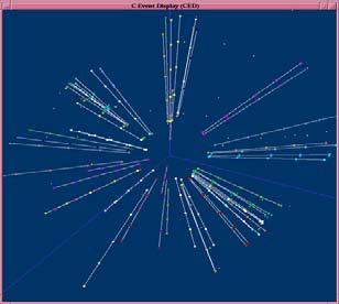
7 Test Beam Setup (at CERN) Bonn University The high precision DEPFET telescope <1 μm track resolution in the DUT plane Error on the predicted position (μm) Using 3 DEPFETs as telescope GEANT Simulation 25 mm 100 mm 250 mm Depfet resolution (μm) Bonn University 5 (!) DEPFET planes, x=25mm
 First results from CERN test beam now available: 120 GeV π, 33x23.75 μm 2 pixels single point resolution 1.")
8 Efficiency & Position resolution Purity = Number of clusters with tracks Total number of clusters Efficiency = Number of tracks with cluster Total number of tracks For 5 σ seed cut Efficiency 99.96% Purity 99.6 % (Jaap Velthuis) First results from CERN test beam now available: 120 GeV π, 33x23.75 μm 2 pixels single point resolution 1.7 μm
9 DEPFET noise at high BW DEPFET Drain First stage: TIA AD kΏ Second stage: AD8129 A=10 Low pass filter ADC Optional: Moving Averaging (FIR) R bias 39kΩ 110MHz Clear ENC < 50e- at 50MHz BW (Stefan Rummel)
 L eff = L - 2 x under etching of 1.")
10 Internal amplification g q g q = di D dq μ = L p ( V 2 GS Vth ) (neglecting short channel effects) (L: nominal gate length) simulation at I D =50 µa g q (pa/e-) g q (pa/e-) effective gate length L eff (µm) L eff = L - 2 x under etching of 1.2µm Drain current I D (µa) (Stefan Rummel) As long as noise is dominated by r/o chip S/N linear with g q PXD4 has L=6μm, some matrices in PXD5 have now L=4μm expect factor 2 better S/N
, April 2007 -: improved input cascode (regulated) and current memory cells -: designed for 40 pf load at the")

11 A new r/o chip - DCD1 DCD: Drain Current Digitizer Test chip: 6X12 channels (pixels) what is new? submitted (UMC 0.18), April : improved input cascode (regulated) and current memory cells -: designed for 40 pf load at the input (1 st layer ILC VTX) -: f/e noise: 34nA@40pF, 17nA@10pF, add 37nA for memory cells 50nA@40pF at 40pF with g q =500pA/e 100 e- ENC in total -: 2 current based ADCs per pixel, 6 bit -: layout for bump bonding (Ivan Peric/Peter Fischer)
 Very small pixels (20µm x 20µm) Increase internal amplification (g q ) Add some bump bonding test structures")
12 New DEPFET Generation PXD5 Mostly use baseline linear DEPFET geometry Build larger matrices Long matrices (full ILC drain length) Wide matrices (full Load for Switcher Gate / Clear chips) Try new DEPFET variants: reduce clear voltages (modified implantations, modified geometry) Very small pixels (20µm x 20µm) Increase internal amplification (g q ) Add some bump bonding test structures standard arrays compatible to existing hybrids wide arrays (512 x 512, full ILC) long arrays (256 x 1024, ½ ILC) 512x512 matrix various new standard arrays (64 x 256 pixels, down to 20x20µm 2 ) Richter, MPI HLL (Rainer Richter)
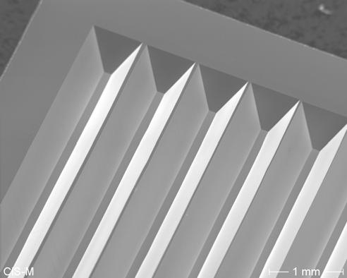
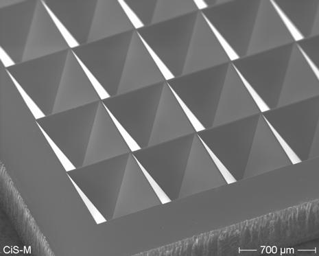
13 Thinning Technology a) oxidation and back side implant of top wafer Top Wafer c) process passivation Handle <100> Wafer open backside passivation b) wafer bonding and grinding/polishing of top wafer d) anisotropic deep etching opens "windows" in handle wafer New: New: New: 150mm Øwafers! Wafer bonding and thinning in industry Compatibility with the main production line tested Still in R&D phase: 1: processing test structures on SOI wafers 2: mechanical samples
14 PiN Diodes on thin Silicon Thin diodes have excellent leakage currents. CV Curve: depletion at 50 V Processing of the SOI wafers and removal of handle wafer does not degrade devices! ρ 150 Ω.cm IV Curve: I rev <8pA at 50 V 20 diodes I rev (50 V): <100pA/cm 2


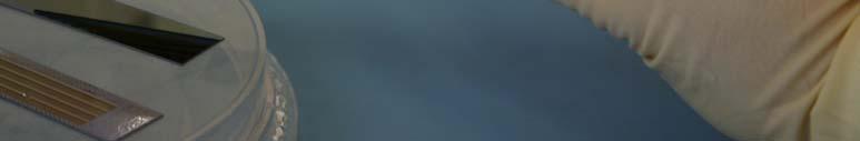
15 Thinning : mechanical samples


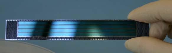
16 Thinning : mechanical samples full size 1 st layer module: 100x13 mm 2 sensitive area, 50 μm thin, 400 μm frame, no support bars 20 μm deflection due to gravity Bill Cooper, FNAL
17 Roadmap Subway map towards a thin demonstrator DEPFET incl. rad. tolerance PXD5 PXD6 Thinning chips/system development CURO3 SWITCHER3 DCD1 full size demonstrator thin Me./El. Samples interconnections on & off module Engineering module/barrels/ discs
18 Summary Matrices operated routinely in test beams at DESY and CERN including a 5 layer DEPFET telescope with sub-micron precision. New sensor production with larger devices and improved DEPFET pixel cells almost finished. Reducing the channel length of the DEPFET translates directly into a higher S/N in the experiment! Dry etching would make it possible to exploit the potential of the DEPFET and is therefore highly desirable! Thinning technology at the door step to migrate to the production line. Excellent results using a commercial supplier for the engineered SOI wafers. We are on schedule for the construction of a full size thin demonstrator by 2010!
ILC requirements Review on CMOS Performances: state of the art Progress on fast read-out sensors & ADC Roadmap for the coming years Summary
 Status on CMOS sensors Auguste Besson on behalf of DAPNIA/Saclay, LPSC/Grenoble, LPC/Clermont-F., DESY, Uni. Hamburg, JINR-Dubna & IPHC/Strasbourg contributions from IPN/Lyon, Uni. Frankfurt, GSI-Darmstadt,
The Alice Silicon Pixel Detector (SPD) Peter Chochula for the Alice Pixel Collaboration
 Peter Chochula for the Alice Pixel Collaboration") The Alice Silicon Pixel Detector (SPD) Peter Chochula for the Alice Pixel Collaboration The Alice Pixel Detector R 1 =3.9 cm R 2 =7.6 cm Main Physics Goal Heavy Flavour Physics D 0 K π+ 15 days Pb-Pb data
The Alice Silicon Pixel Detector (SPD) Peter Chochula for the Alice Pixel Collaboration The Alice Pixel Detector R 1 =3.9 cm R 2 =7.6 cm Main Physics Goal Heavy Flavour Physics D 0 K π+ 15 days Pb-Pb data
Performance of a double-metal n-on-n and a Czochralski silicon strip detector read out at LHC speeds
 Performance of a double-metal n-on-n and a Czochralski silicon strip detector read out at LHC speeds Juan Palacios, On behalf of the LHCb VELO group J.P. Palacios, Liverpool Outline LHCb and VELO performance
ISC0904: 1k x 1k 18µm N-on-P ROIC. Specification January 13, 2012
 ISC0904 1k x 1k 18µm N-on-P ROIC Specification January 13, 2012 This presentation contains content that is proprietary to FLIR Systems. Information is subject to change without notice. 1 Version 1.00 January
The Silicon Pixel Detector (SPD) for the ALICE Experiment
 for the ALICE Experiment") The Silicon Pixel Detector (SPD) for the ALICE Experiment V. Manzari/INFN Bari, Italy for the SPD Project in the ALICE Experiment INFN and Università Bari, Comenius University Bratislava, INFN and Università
The Silicon Pixel Detector (SPD) for the ALICE Experiment V. Manzari/INFN Bari, Italy for the SPD Project in the ALICE Experiment INFN and Università Bari, Comenius University Bratislava, INFN and Università
The ATLAS Pixel Chip FEI in 0.25µm Technology
 The ATLAS Pixel Chip FEI in 0.25µm Technology Peter Fischer, Universität Bonn (for Ivan Peric) for the ATLAS pixel collaboration The ATLAS Pixel Chip FEI Short Introduction to ATLAS Pixel mechanics, modules
Note on the preliminary organisation for the design, fabrication and test of a prototype double-sided ladder equipped with MAPS
 Note on the preliminary organisation for the design, fabrication and test of a prototype double-sided ladder equipped with MAPS J.Baudot a, J.Goldstein b, A.Nomerotski c, M.Winter a a IPHC - Université
The FEL detector development program at DESY. Heinz Graafsma DESY-Photon Science Detector Group WorkPackage Detectors for XFEL
 The FEL detector development program at DESY DESY-Photon Science Detector Group WorkPackage Detectors for XFEL EUROFEL-2009 Hard X-ray SASE Free Electron Lasers LINAC COHERENT LIGHT SOURCE LCLS 2009 2010
Concept and operation of the high resolution gaseous micro-pixel detector Gossip
 Concept and operation of the high resolution gaseous micro-pixel detector Gossip Yevgen Bilevych 1,Victor Blanco Carballo 1, Maarten van Dijk 1, Martin Fransen 1, Harry van der Graaf 1, Fred Hartjes 1,
Sensors for the CMS High Granularity Calorimeter
 Sensors for the CMS High Granularity Calorimeter Andreas Alexander Maier (CERN) on behalf of the CMS Collaboration Wed, March 1, 2017 The CMS HGCAL project ECAL Answer to HL-LHC challenges: Pile-up: up
A new Scintillating Fibre Tracker for LHCb experiment
 A new Scintillating Fibre Tracker for LHCb experiment Alexander Malinin, NRC Kurchatov Institute on behalf of the LHCb-SciFi-Collaboration Instrumentation for Colliding Beam Physics BINP, Novosibirsk,
Atlas Pixel Replacement/Upgrade. Measurements on 3D sensors
 Atlas Pixel Replacement/Upgrade and Measurements on 3D sensors Forskerskole 2007 by E. Bolle erlend.bolle@fys.uio.no Outline Sensors for Atlas pixel b-layer replacement/upgrade UiO activities CERN 3D test
The hybrid photon detectors for the LHCb-RICH counters
 7 th International Conference on Advanced Technology and Particle Physics The hybrid photon detectors for the LHCb-RICH counters Maria Girone, CERN and Imperial College on behalf of the LHCb-RICH group
TORCH a large-area detector for high resolution time-of-flight
 TORCH a large-area detector for high resolution time-of-flight Roger Forty (CERN) on behalf of the TORCH collaboration 1. TORCH concept 2. Application in LHCb 3. R&D project 4. Test-beam studies TIPP 2017,
A pixel chip for tracking in ALICE and particle identification in LHCb
 A pixel chip for tracking in ALICE and particle identification in LHCb K.Wyllie 1), M.Burns 1), M.Campbell 1), E.Cantatore 1), V.Cencelli 2) R.Dinapoli 3), F.Formenti 1), T.Grassi 1), E.Heijne 1), P.Jarron
TPC R&D by LCTPC. Organisation, results, plans. Jan Timmermans NIKHEF & DESY(2009) On behalf of the LCTPC Collaboration TILC09, Tsukuba
 On behalf of the LCTPC Collaboration TILC09, Tsukuba") TPC R&D by LCTPC Organisation, results, plans Jan Timmermans NIKHEF & DESY(2009) On behalf of the LCTPC Collaboration TILC09, Tsukuba 20 April, 2009 LCTPC Collaboration IIHE ULB-VUB Brussels 2 LCTPC Collaboration
TPC R&D by LCTPC Organisation, results, plans Jan Timmermans NIKHEF & DESY(2009) On behalf of the LCTPC Collaboration TILC09, Tsukuba 20 April, 2009 LCTPC Collaboration IIHE ULB-VUB Brussels 2 LCTPC Collaboration
Results on 0.7% X0 thick Pixel Modules for the ATLAS Detector.
 Results on 0.7% X0 thick Pixel Modules for the ATLAS Detector. INFN Genova: R.Beccherle, G.Darbo, G.Gagliardi, C.Gemme, P.Netchaeva, P.Oppizzi, L.Rossi, E.Ruscino, F.Vernocchi Lawrence Berkeley National
HAPD and Electronics Updates
 S. Nishida KEK 3rd Open Meeting for Belle II Collaboration 1 Contents Frontend Electronics Neutron Irradiation News from Hamamtsu 2 144ch HAPD HAPD (Hybrid Avalanche Photo Detector) photon bi alkali photocathode
CGEM-IT project update
 BESIII Physics and Software Workshop Beihang University February 20-23, 2014 CGEM-IT project update Gianluigi Cibinetto (INFN Ferrara) on behalf of the CGEM group Outline Introduction Mechanical development
Monolithic Thin Pixel Upgrade Testing Update. Gary S. Varner, Marlon Barbero and Fang Fang UH Belle Meeting, April 16 th 2004
 Monolithic Thin Pixel Upgrade Testing Update Gary S. Varner, Marlon Barbero and Fang Fang UH Belle Meeting, April 16 th 2004 Basic Technology: Standard CMOS CMOS Camera Because of large Capacitance, need
CMS Note Mailing address: CMS CERN, CH-1211 GENEVA 23, Switzerland
 Available on CMS information server CMS NOTE 1999/012 The Compact Muon Solenoid Experiment CMS Note Mailing address: CMS CERN, CH-1211 GENEVA 23, Switzerland February 23, 1999 Assembly and operation of
Gated mode operation with Hybrid 5
 Gated mode operation with Hybrid 5 J. Dingfelder, L. Germic, T. Hemperek, Jan Cedric Hönig, H. Krüger, F. Lütticke, C. Marinas, B. Paschen, N. Wermes Gated Mode operation Continuous injection of particles
The ATLAS Pixel Detector
 The ATLAS Pixel Detector Fabian Hügging arxiv:physics/0412138v2 [physics.ins-det] 5 Aug 5 Abstract The ATLAS Pixel Detector is the innermost layer of the ATLAS tracking system and will contribute significantly
SciFi A Large Scintillating Fibre Tracker for LHCb
 SciFi A Large Scintillating Fibre Tracker for LHCb Roman Greim on behalf of the LHCb-SciFi-Collaboration 14th Topical Seminar on Innovative Particle Radiation Detectors, Siena 5th October 2016 I. Physikalisches
Overview of All Pixel Circuits for Active Matrix Organic Light Emitting Diode (AMOLED)
") Chapter 2 Overview of All Pixel Circuits for Active Matrix Organic Light Emitting Diode (AMOLED) ---------------------------------------------------------------------------------------------------------------
Chapter 2 Overview of All Pixel Circuits for Active Matrix Organic Light Emitting Diode (AMOLED) ---------------------------------------------------------------------------------------------------------------
CMS Upgrade Activities
 CMS Upgrade Activities G. Eckerlin DESY WA, 1. Feb. 2011 CMS @ LHC CMS Upgrade Phase I CMS Upgrade Phase II Infrastructure Conclusion DESY-WA, 1. Feb. 2011 G. Eckerlin 1 The CMS Experiments at the LHC
ILC Detector Work. Dan Peterson
 ILC Detector Work Dan Peterson ** Cornell/Purdue TPC development program Large Detector Concept TPC Detector Response Simulation and Track Reconstruction World Wide Study Detector R&D Panel This project
A Review of Tracking Sessions
 A Review of Tracking Sessions Madhu S. Dixit TRIUMF & Carleton University Durham ECFA Workshop 1-4 September 2004 8 minutes time for this summary (allow 2 minutes for questions) 3 tracking sessions lasting
RX40_V1_0 Measurement Report F.Faccio
 RX40_V1_0 Measurement Report F.Faccio This document follows the previous report An 80Mbit/s Optical Receiver for the CMS digital optical link, dating back to January 2000 and concerning the first prototype
Drift Tubes as Muon Detectors for ILC
 Drift Tubes as Muon Detectors for ILC Dmitri Denisov Fermilab Major specifications for muon detectors D0 muon system tracking detectors Advantages and disadvantages of drift chambers as muon detectors
Readout techniques for drift and low frequency noise rejection in infrared arrays
 Readout techniques for drift and low frequency noise rejection in infrared arrays European Southern Observatory Finger, G., Dorn, R.J, Hoffman, A.W., Mehrgan, H., Meyer, M., Moorwood, A.F.M., Stegmeier,
li, o p a f th ed lv o v ti, N sca reb g s In tio, F, Z stitu e tests o e O v o d a eters sin u i P r th e d est sezio tefa ectro lity stem l su
 Design and prototype tests of the system for the OPERA spectrometers Stefano Dusini INFN sezione di Padova Outline OPERA Detector Inner Tracker Design Mechanical support Gas & HV Production and Quality
The Status of the ATLAS Inner Detector
 The Status of the ATLAS Inner Detector Introduction Hans-Günther Moser for the ATLAS Collaboration Outline Tracking in ATLAS ATLAS ID Pixel detector Silicon Tracker Transition Radiation Tracker System
FRONT-END AND READ-OUT ELECTRONICS FOR THE NUMEN FPD
 FRONT-END AND READ-OUT ELECTRONICS FOR THE NUMEN FPD D. LO PRESTI D. BONANNO, F. LONGHITANO, D. BONGIOVANNI, S. REITO INFN- SEZIONE DI CATANIA D. Lo Presti, NUMEN2015 LNS, 1-2 December 2015 1 OVERVIEW
A Cylindrical GEM Detector with Analog Readout for the BESIII Experiment. Gianluigi Cibinetto (INFN Ferrara) on behalf of the BESIIICGEM consortium
 on behalf of the BESIIICGEM consortium") A Cylindrical GEM Detector with Analog Readout for the BESIII Experiment Gianluigi Cibinetto (INFN Ferrara) on behalf of the BESIIICGEM consortium Outline The BESIII experiment the Inner tracker The BESIII
A Cylindrical GEM Detector with Analog Readout for the BESIII Experiment Gianluigi Cibinetto (INFN Ferrara) on behalf of the BESIIICGEM consortium Outline The BESIII experiment the Inner tracker The BESIII
Mimosa32: Tower CIS October 2011 submission: 4 Metal, MiM Capacitor, Quadruple Well (deep-n and deep-p wells), HR epi
, HR epi") 3.3 Discri-per-pix 80x25 array 16x80 µm JTAG structure SPAD Mimosa32: Tower CIS October 2011 submission: 4 Metal, MiM Capacitor, Quadruple Well (deep-n and deep-p wells), HR epi - Overall chip dimension:
3.3 Discri-per-pix 80x25 array 16x80 µm JTAG structure SPAD Mimosa32: Tower CIS October 2011 submission: 4 Metal, MiM Capacitor, Quadruple Well (deep-n and deep-p wells), HR epi - Overall chip dimension:
 Chapter 3 Evaluated Results of Conventional Pixel Circuit, Other Compensation Circuits and Proposed Pixel Circuits for Active Matrix Organic Light Emitting Diodes (AMOLEDs) -------------------------------------------------------------------------------------------------------
The CALICE test beam programme
 Journal of Physics: Conference Series The CALICE test beam programme To cite this article: F Salvatore 2009 J. Phys.: Conf. Ser. 160 012064 View the article online for updates and enhancements. Related
Status of CMS Silicon Strip Tracker
 1 Status of CMS Silicon Strip Tracker N. Demaria a on behalf of the CMS Tracker Collaboration a INFN Sez. di Torino, v. P.Giuria 1, I-10125 Torino Italy E-mail: Natale.Demaria@to.infn.it The CMS Silicon
Large Area, High Speed Photo-detectors Readout
 Large Area, High Speed Photo-detectors Readout Jean-Francois Genat + On behalf and with the help of Herve Grabas +, Samuel Meehan +, Eric Oberla +, Fukun Tang +, Gary Varner ++, and Henry Frisch + + University
Review of the CMS muon detector system
 1 Review of the CMS muon detector system E. Torassa a a INFN sez. di Padova, Via Marzolo 8, 35131 Padova, Italy The muon detector system of CMS consists of 3 sub detectors, the barrel drift tube chambers
THE ATLAS Inner Detector [2] is designed for precision
![THE ATLAS Inner Detector [2] is designed for precision](/thumbs/79/79327554.jpg "THE ATLAS Inner Detector [2] is designed for precision") The ATLAS Pixel Detector Fabian Hügging on behalf of the ATLAS Pixel Collaboration [1] arxiv:physics/412138v1 [physics.ins-det] 21 Dec 4 Abstract The ATLAS Pixel Detector is the innermost layer of the
The ATLAS Pixel Detector Fabian Hügging on behalf of the ATLAS Pixel Collaboration [1] arxiv:physics/412138v1 [physics.ins-det] 21 Dec 4 Abstract The ATLAS Pixel Detector is the innermost layer of the
Beam test of the QMB6 calibration board and HBU0 prototype
 Beam test of the QMB6 calibration board and HBU0 prototype J. Cvach 1, J. Kvasnička 1,2, I. Polák 1, J. Zálešák 1 May 23, 2011 Abstract We report about the performance of the HBU0 board and the optical
Research Results in Mixed Signal IC Design
 Research Results in Mixed Signal IC Design Jiren Yuan, Professor Department of Electroscience Lund University, Lund, Sweden J. Yuan, Dept. of Electroscience, Lund University 1 Work packages in project
arxiv: v1 [physics.ins-det] 2 Dec 2008
![arxiv: v1 [physics.ins-det] 2 Dec 2008](/thumbs/88/115175701.jpg "arxiv: v1 [physics.ins-det] 2 Dec 2008") arxiv:0812.0454v1 [physics.ins-det] 2 Dec 2008 A Scintillating Fiber Tracker With SiPM Readout G. Roper Yearwood a, B. Beischer a, Ch.-H. Chung a, Ph. v. Doetinchem a, H. Gast a, R. Greim a, T. Kirn a,
arxiv:0812.0454v1 [physics.ins-det] 2 Dec 2008 A Scintillating Fiber Tracker With SiPM Readout G. Roper Yearwood a, B. Beischer a, Ch.-H. Chung a, Ph. v. Doetinchem a, H. Gast a, R. Greim a, T. Kirn a,
A FOUR GAIN READOUT INTEGRATED CIRCUIT : FRIC 96_1
 A FOUR GAIN READOUT INTEGRATED CIRCUIT : FRIC 96_1 J. M. Bussat 1, G. Bohner 1, O. Rossetto 2, D. Dzahini 2, J. Lecoq 1, J. Pouxe 2, J. Colas 1, (1) L. A. P. P. Annecy-le-vieux, France (2) I. S. N. Grenoble,
Advanced Training Course on FPGA Design and VHDL for Hardware Simulation and Synthesis. 26 October - 20 November, 2009
 2065-28 Advanced Training Course on FPGA Design and VHDL for Hardware Simulation and Synthesis 26 October - 20 November, 2009 Starting to make an FPGA Project Alexander Kluge PH ESE FE Division CERN 385,
Data Sheet. MGA GHz WLAN Power Amplifier Module. Description. Features. Component Image. Applications. Pin Configuration
 MGA-43024 2.4 GHz WLAN Power Amplifier Module Data Sheet Description Avago Technologies MGA-43024 is a fully matched power amplifier for use in the WLAN band (2401-2484 MHz). High linear output power at
Scintillation Tile Hodoscope for the PANDA Barrel Time-Of-Flight Detector
 Scintillation Tile Hodoscope for the PANDA Barrel Time-Of-Flight Detector William Nalti, Ken Suzuki, Stefan-Meyer-Institut, ÖAW on behalf of the PANDA/Barrel-TOF(SciTil) group 12.06.2018, ICASiPM2018 1
The TDCPix ASIC: Tracking for the NA62 GigaTracker. G. Aglieri Rinella, S. Bonacini, J. Kaplon, A. Kluge, M. Morel, L. Perktold, K.
 : Tracking for the NA62 GigaTracker CERN E-mail: matthew.noy@cern.ch G. Aglieri Rinella, S. Bonacini, J. Kaplon, A. Kluge, M. Morel, L. Perktold, K. Poltorak CERN The TDCPix is a hybrid pixel detector
Status of readout electronic design in MOST1
 Status of readout electronic design in MOST1 Na WANG, Ke WANG, Zhenan LIU, Jia TAO On behalf of the Trigger Group (IHEP) Mini-workshop for CEPC MOST silicon project,23 November,2017,Beijing Outline Introduction
Advanced Front End Signal Processing Electronics for ATLAS CSC System: Status And Post Production Performance.
 Advanced Front End Signal Processing Electronics for ATLAS CSC System: Status And Post Production Performance. Sachin S Junnarkar, Anand Kandasamy, Paul O Connor Brookhaven National Laboratory, Upton,
PICOSECOND TIMING USING FAST ANALOG SAMPLING
 PICOSECOND TIMING USING FAST ANALOG SAMPLING H. Frisch, J-F Genat, F. Tang, EFI Chicago, Tuesday 6 th Nov 2007 INTRODUCTION In the context of picosecond timing, analog detector pulse sampling in the 10
High ResolutionCross Strip Anodes for Photon Counting detectors
 High ResolutionCross Strip Anodes for Photon Counting detectors Oswald H.W. Siegmund, Anton S. Tremsin, Robert Abiad, J. Hull and John V. Vallerga Space Sciences Laboratory University of California Berkeley,
NMOS linear image sensor
 Image sensor highly sensitive to X-rays from 0 k to 00 kev s are self-scanning photodiode arrays designed specifically as detectors for multichannel spectroscopy. The scanning circuit is made up of N-channel
Reading a GEM with a VLSI pixel ASIC used as a direct charge collecting anode. R.Bellazzini - INFN Pisa. Vienna February
 Reading a GEM with a VLSI pixel ASIC used as a direct charge collecting anode Ronaldo Bellazzini INFN Pisa Vienna February 16-21 2004 The GEM amplifier The most interesting feature of the Gas Electron
Report from the Tracking and Vertexing Group:
 Report from the Tracking and Vertexing Group: October 10, 2016 Sally Seidel, Petra Merkel, Maurice Garcia- Sciveres Structure of parallel session n Silicon Sensor Fabrication on 8 wafers (Ron Lipton) n
CCD 143A 2048-Element High Speed Linear Image Sensor
 A CCD 143A 2048-Element High Speed Linear Image Sensor FEATURES 2048 x 1 photosite array 13µm x 13µm photosites on 13µm pitch High speed = up to 20MHz data rates Enhanced spectral response Low dark signal
Silicon Drift Detectors for the NLC
 Silicon Drift Detectors for the NLC Rene Bellwied (Wayne State University) SD Tracking Meeting September 18th, 2003 Proposed layout for LC tracker Silicon Drift technology hardware progress & plans SVT
Prototype of a Gigabit Data Transmitter in 65-nm CMOS for DEPFET Pixel Detectors at Belle-II
 Prototype of a Gigabit Data Transmitter in 65-nm CMOS for DEPFET Pixel Detectors at Belle-II Tetsuichi Kishishita H. Krüger, T. Hemperek, M. Lemarenko, M. Koch, M. Gronewald, N. Wermes University of Bonn
Electronics procurements
 Electronics procurements 24 October 2014 Geoff Hall Procurements from CERN There are a wide range of electronics items procured by CERN but we are familiar with only some of them Probably two main categories:
Photodiode Detector with Signal Amplification
 107 Bonaventura Dr., San Jose, CA 95134 Tel: +1 408 432 9888 Fax: +1 408 432 9889 www.x-scanimaging.com Linear X-Ray Photodiode Detector Array with Signal Amplification XB8801R Series An X-Scan Imaging
CCD220 Back Illuminated L3Vision Sensor Electron Multiplying Adaptive Optics CCD
 CCD220 Back Illuminated L3Vision Sensor Electron Multiplying Adaptive Optics CCD FEATURES 240 x 240 pixel image area 24 µm square pixels Split frame transfer 100% fill factor Back-illuminated for high
Wafer Thinning and Thru-Silicon Vias
 Wafer Thinning and Thru-Silicon Vias The Path to Wafer Level Packaging jreche@trusi.com Summary A new dry etching technology Atmospheric Downstream Plasma (ADP) Etch Applications to Packaging Wafer Thinning
The Large TPC Prototype: Infrastructure/ Status/ Plans
 The Large TPC Prototype: Infrastructure/ Status/ Plans Takeshi Matsuda, KEK/ DESY Ties Behnke, DESY For the LC-TPC collaboration Status of the test beam infrastructure Status of the Large Prototype Field
Silicon Microstrip Detectors for the ATLAS SCT
 Silicon Microstrip Detectors for the ATLAS SCT D. Robinson, Cavendish Laboratory for the ATLAS SCT 5th International Conference on Large Scale Applications and Radiation Hardness of Semiconductor Detectors
P ixel Detector Module using MC M-D Technology for the B -layer of the AT LAS P ixel Detector
 P ixel Detector Module using MC M-D Technology for the B -layer of the AT LAS P ixel Detector DETECTOR CHIP Pixel 2000 Workshop O. Bäsken K.H.Becks P.Gerlach Ch. Grah O.Ehrmann M.Töpper J.Wolf Christian
PIXEL2000, June 5-8, FRANCO MEDDI CERN-ALICE / University of Rome & INFN, Italy. For the ALICE Collaboration
 PIXEL2000, June 5-8, 2000 FRANCO MEDDI CERN-ALICE / University of Rome & INFN, Italy For the ALICE Collaboration CONTENTS: Introduction: Physics Requirements Design Considerations Present development status
HARDROC, Readout chip of the Digital Hadronic Calorimeter of ILC
 HARDROC, Readout chip of the Digital Hadronic Calorimeter of ILC S. Callier a, F. Dulucq a, C. de La Taille a, G. Martin-Chassard a, N. Seguin-Moreau a a OMEGA/LAL/IN2P3, LAL Université Paris-Sud, Orsay,France
3D-CHIP TECHNOLOGY AND APPLICATIONS OF MINIATURIZATION
 3D-CHIP TECHNOLOGY AND APPLICATIONS OF MINIATURIZATION 23.08.2018 I DAVID ARUTINOV CONTENT INTRODUCTION TRENDS AND ISSUES OF MODERN IC s 3D INTEGRATION TECHNOLOGY CURRENT STATE OF 3D INTEGRATION SUMMARY
Advanced Implantation Detector Array (AIDA) Second BRIKEN Workshop RIKEN July 2013
 Second BRIKEN Workshop RIKEN July 2013") Advanced Implantation Detector Array (AIDA) Second BRIKEN Workshop RIKEN 30-31 July 2013 presented by Tom Davinson on behalf of the AIDA collaboration (Edinburgh Liverpool STFC DL & RAL) Tom Davinson School
Advanced Implantation Detector Array (AIDA) Second BRIKEN Workshop RIKEN 30-31 July 2013 presented by Tom Davinson on behalf of the AIDA collaboration (Edinburgh Liverpool STFC DL & RAL) Tom Davinson School
CCD Element Linear Image Sensor CCD Element Line Scan Image Sensor
 1024-Element Linear Image Sensor CCD 134 1024-Element Line Scan Image Sensor FEATURES 1024 x 1 photosite array 13µm x 13µm photosites on 13µm pitch Anti-blooming and integration control Enhanced spectral
The Readout Architecture of the ATLAS Pixel System
 The Readout Architecture of the ATLAS Pixel System Roberto Beccherle / INFN - Genova E-mail: Roberto.Beccherle@ge.infn.it Copy of This Talk: http://www.ge.infn.it/atlas/electronics/home.html R. Beccherle
with Low Cost and Low Material Budget
 Gaseous Beam Position Detectors, with Low Cost and Low Material Budget Gyula Bencédi on behalf of the REGaRD group MTA KFKI RMKI, ELTE November 29, 2011, Outline Physics Motivation Newish MWPCs, the Close
Status of the Front Tracker GEM and INFN Electronics
 Status of the Front Tracker GEM and INFN Electronics 2013 Apr 10 SBS Weekly Meeting INFN Catania, Genova, Bari and Rome GEM Production First Tests on module 0 Improvements in design Electronics Continue
LHC Beam Instrumentation Further Discussion
 LHC Beam Instrumentation Further Discussion LHC Machine Advisory Committee 9 th December 2005 Rhodri Jones (CERN AB/BDI) Possible Discussion Topics Open Questions Tune measurement base band tune & 50Hz
R&D plan for ILC(ILD) TPC in (LC TPC Collaboration)
 TPC in (LC TPC Collaboration)") R&D plan for ILC(ILD) TPC in 2010-2012 (LC TPC Collaboration) LCWA09 Tracker Session 02 October 2009 LC TPC Collaboration Takeshi MATSUDA DESY/FLC 1 R&D Goals for ILC (ILD) TPC High Momentum resolution:
R&D plan for ILC(ILD) TPC in 2010-2012 (LC TPC Collaboration) LCWA09 Tracker Session 02 October 2009 LC TPC Collaboration Takeshi MATSUDA DESY/FLC 1 R&D Goals for ILC (ILD) TPC High Momentum resolution:
Local Trigger Electronics for the CMS Drift Tubes Muon Detector
 Amsterdam, 1 October 2003 Local Trigger Electronics for the CMS Drift Tubes Muon Detector Presented by R.Travaglini INFN-Bologna Italy CMS Drift Tubes Muon Detector CMS Barrel: 5 wheels Wheel : Azimuthal
Jean-Claude Brient Laboratoire Leprince-Ringuet
 Jean-Claude Brient Laboratoire Leprince-Ringuet Collaboration between IN2P3 laboratories (LLR LAL LPSC LPNHE Omega) & Japan institutes (University of Kyushu, KEK ) More specific thanks to M.Anduze, V.Boudry,
The field cage for a large TPC prototype
 EUDET The field cage for a large TPC prototype T.Behnke, L. Hallermann, P. Schade, R. Diener December 7, 2006 Abstract Within the EUDET Programme, the FLC TPC Group at DESY in collaboration with the Department
V6118 EM MICROELECTRONIC - MARIN SA. 2, 4 and 8 Mutiplex LCD Driver
 EM MICROELECTRONIC - MARIN SA 2, 4 and 8 Mutiplex LCD Driver Description The is a universal low multiplex LCD driver. The version 2 drives two ways multiplex (two blackplanes) LCD, the version 4, four
CAEN Tools for Discovery
 Viareggio March 28, 2011 Introduction: what is the SiPM? The Silicon PhotoMultiplier (SiPM) consists of a high density (up to ~10 3 /mm 2 ) matrix of diodes connected in parallel on a common Si substrate.
In-process inspection: Inspector technology and concept
 Inspector In-process inspection: Inspector technology and concept Need to inspect a part during production or the final result? The Inspector system provides a quick and efficient method to interface a
First evaluation of the prototype 19-modules camera for the Large Size Telescope of the CTA
 First evaluation of the prototype 19-modules camera for the Large Size Telescope of the CTA Tsutomu Nagayoshi for the CTA-Japan Consortium Saitama Univ, Max-Planck-Institute for Physics 1 Cherenkov Telescope
FPGA Based Data Read-Out System of the Belle 2 Pixel Detector
 FPGA Based Read-Out System of the Belle 2 Pixel Detector Dmytro Levit, Igor Konorov, Daniel Greenwald, Stephan Paul Technische Universität München arxiv:1406.3864v1 [physics.ins-det] 15 Jun 2014 Abstract
and progress report first mip measurement with a complete chain of detector slab Silicon wafers for the prototype Mechanics PCB for prototype
 progress report Silicon wafers for the prototype Mechanics PCB for prototype VFE electronics DAQ Simulation and analysis and first mip measurement with a complete chain of detector slab Report prepared
Mechanical Considerations in the Outer Tracker and VXD. Bill Cooper Fermilab
 Mechanical Considerations in the Outer Tracker and VXD Fermilab August 23, 2005 1 Overview I ll describe developments since the SLAC workshop in mechanical design efforts at Fermilab related to SiD tracking.
An extreme high resolution Timing Counter for the MEG Upgrade
 An extreme high resolution Timing Counter for the MEG Upgrade M. De Gerone INFN Genova on behalf of the MEG collaboration 13th Topical Seminar on Innovative Particle and Radiation Detectors Siena, Oct.
SuperFRS GEM-TPC Development Status Report
 SuperFRS GEM-TPC Development Status Report COLLABORATORS F. García, R. Turpeinen, J. Heino, A. Karadzhinova, E. Tuominen, R. Lauhakangas Helsinki Institute of Physics University of Helsinki - Finland R.
Flexible Electronics Production Deployment on FPD Standards: Plastic Displays & Integrated Circuits. Stanislav Loboda R&D engineer
 Flexible Electronics Production Deployment on FPD Standards: Plastic Displays & Integrated Circuits Stanislav Loboda R&D engineer The world-first small-volume contract manufacturing for plastic TFT-arrays
TPC R&D at Cornell and Purdue
 TPC R&D at Cornell and Purdue Cornell University Purdue University T. Anous K. Arndt R. S. Galik G. Bolla D. P. Peterson I. P. J. Shipsey J. Ledoux Further information available at the web sites: http://www.lepp.cornell.edu/~dpp/linear_collider/large_prototype.html
RF considerations for SwissFEL
 RF considerations for H. Fitze in behalf of the PSI RF group Workshop on Compact X-Ray Free Electron Lasers 19.-21. July 2010, Shanghai Agenda Introduction RF-Gun Development C-band development Summary
Mahdad Manavi LOTS Technology, Inc.
 Presented by Mahdad Manavi LOTS Technology, Inc. 1 Authors: Mahdad Manavi, Aaron Wegner, Qi-Ze Shu, Yeou-Yen Cheng Special Thanks to: Dan Soo, William Oakley 2 25 MB/sec. user data transfer rate for both
Digital BPMs and Orbit Feedback Systems
 Digital BPMs and Orbit Feedback Systems, M. Böge, M. Dehler, B. Keil, P. Pollet, V. Schlott Outline stability requirements at SLS storage ring digital beam position monitors (DBPM) SLS global fast orbit
Integrating Silicon tracking in ILC detector concepts: solutions & challenges
 Integrating Silicon tracking in ILC detector concepts: solutions & challenges Aurore Savoy Navarro, LPNHE Universite Pierre et Marie Curie/IN2P3 CNRS The work reported here is done within the SiLC R&D
Commissioning and Performance of the ATLAS Transition Radiation Tracker with High Energy Collisions at LHC
 Commissioning and Performance of the ATLAS Transition Radiation Tracker with High Energy Collisions at LHC 1 A L E J A N D R O A L O N S O L U N D U N I V E R S I T Y O N B E H A L F O F T H E A T L A
Compact Muon Solenoid Detector (CMS) & The Token Bit Manager (TBM) Alex Armstrong & Wyatt Behn Mentor: Dr. Andrew Ivanov
 & The Token Bit Manager (TBM) Alex Armstrong & Wyatt Behn Mentor: Dr. Andrew Ivanov") Compact Muon Solenoid Detector (CMS) & The Token Bit Manager (TBM) Alex Armstrong & Wyatt Behn Mentor: Dr. Andrew Ivanov Part 1: The TBM and CMS Understanding how the LHC and the CMS detector work as a
Compact Muon Solenoid Detector (CMS) & The Token Bit Manager (TBM) Alex Armstrong & Wyatt Behn Mentor: Dr. Andrew Ivanov Part 1: The TBM and CMS Understanding how the LHC and the CMS detector work as a
Current status of Hamamatsu Si detectors mainly for High Energy Physics Experiments
 Current status of Hamamatsu Si detectors mainly for High Energy Physics Experiments HAMAMATSU PHOTONICS K.K. K.Yamamura S.Kamada* December 2017 Solid State Division Outline 1/32 1. SSD (Silicon Strip Detector)
CCD Datasheet Electron Multiplying CCD Sensor Back Illuminated, 1024 x 1024 Pixels 2-Phase IMO
 CCD351-00 Datasheet Electron Multiplying CCD Sensor Back Illuminated, 1024 x 1024 Pixels 2-Phase IMO MAIN FEATURES 1024 x 1024 active pixels 10µm square pixels Variable multiplicative gain Frame rates
FRANCO MEDDI CERN-ALICE / University of Rome & INFN, Italy. For the ALICE Collaboration
 PIXEL2000, June 5-8, 2000 FRANCO MEDDI CERN-ALICE / University of Rome & INFN, Italy For the ALICE Collaboration JUNE 5-8,2000 PIXEL2000 1 CONTENTS: Introduction: Physics Requirements Design Considerations