CDA 4253 FPGA System Design FPGA Architectures. Hao Zheng Dept of Comp Sci & Eng U of South Florida
|
|
|
- Eunice Booth
- 6 years ago
- Views:
Transcription
1 CDA 4253 FPGA System Design FPGA Architectures Hao Zheng Dept of Comp Sci & Eng U of South Florida

2 FPGAs Generic Architecture Also include common fixed logic blocks for higher performance: On-chip mem. DSP/MulHplier Fast arithmehc logic Microprocessors CommunicaHon logic
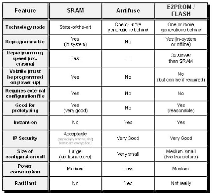
3 Programming Technologies
4 Programming Technologies: Fuses
5 Programming Technologies: Fuses
6 Programming Technologies: An?-fuses
7 Programming Technologies: An?-fuses
8 Programming Technologies: FLASH
9 Programming Technologies: SRAM Transistor SRAM 1 0 Open Closed


10 Sta?c RAM Cell
11
12 Basic Logic Elements (BLEs) Basic component that can be programmed to logic funchons and provide storage.
13 Lookup Tables (LUTs) SRAM SRAM SRAM SRAM x y Commercial FPGAs Xilinx: 6-LUT Altera: 6-LUT Microsemi: 4-LUT For x-input LUT, it can be programmed into one of funchons. 2 2x
14 LUT = Programmable Truth Table x y x y z A B C z 0 0 A 0 1 B 1 0 C 1 1 D D 11 Also called funchon generator.
15 AND x y x y z z
16 OR x y x y z z
17 NAND x y x y z z
18 NOR x y x y z z
19 XOR XNOR x y x y z z 11 11
20 z = y z = y + x x y x y z z 11 11
21 Features of LUTs A LUT is a piece of RAM. Can be configured as distributed RAM in Xilinx. Can be configured as shix registers. A n-lut can implement any n-input logic funchons. Logic minimizahon should reduce the number of inputs, not logical operators. All logic funchons implemented by a n-lut have the same propagahon delay.
22 Look-up-tables (LUTs) Why aren t FPGAs just a big LUT? Size of truth table grows exponentially based on # of inputs 3 inputs = 8 rows, 4 inputs = 16 rows, 5 inputs = 32 rows, etc. Same number of rows in truth table and LUT LUTs grow exponentially based on # of inputs Number of SRAM bits in a LUT = 2 i * o i = # of inputs, o = # of outputs Example: 64 input combinational logic with 1 output would require 2 64 SRAM bits 1.84 x SRAM bits required. Clearly, not feasible to use large LUTs So, how do FPGAs implement logic with many inputs?
23 Look-up-tables (LUTs) Map circuits onto multiple LUTs Divide circuit into smaller circuits that fit in LUTs (same # of inputs and outputs) Example: 2-input LUTs

24 Configurable Logic Blocks Number of BLEs are grouped with a local network in order to implement funchons with a large number of inputs and mulhple outputs.
25 Configurable Logic Blocks (CLBs) Example: Ripple-carry adder Each LUT implements 1 full adder Use efficient connections between LUTs for carry signals A(1) B(1) A(0) B(0) Cin(0) 2x1 Cin(1) CLB 3-in, 2-out LUT 3-in, 2-out LUT FF FF FF FF 2x1 2x1 Cout(0) 2x1 2x1 Cout(1) S(1) S(0)
26 Programmable Interconnect

27 FPGA Rou?ng Architectures Must be flexible to accommodate various circuit implementa6ons.

28 Connec?on Boxes Programmable switches SRAM

29 Switch Boxes SRAM cell
30 Segmented Rou?ng Short wires: many, local connechons. Long wires: few, low latency, carrying global signals Dedicated long wires for clock/reset signals

31 Hierarchical Rou?ng Architecture Most designs display locality of connec6ons hierarchical rou6ng architecture.

32 FPGA Configura?on

33 Configura?on Comes at a Cost 1T 6T SRAM 4-6 T SRAM 4T SRAM + ConfiguraHon circuitry + Error detechon/correchon + Security features h^ps://en.wikipedia.org/wiki/stahc_randomaccess_memory
34 FPGA Design Flow
35 FPGA CAD Flow Input: A circuit (netlist) Output: FPGA configurahon bitstream Main (Algorithmic) Stages: Logic synthesis/ophmizahon Technology mapping Packing/placement RouHng Bitstream generahon
36 Xilinx FPGA Architecture DS099-1_01_032703


37 Xilinx 7-Series FPGA Architecture Precise, Low Ji^er Clocking On-Chip block RAM On-Chip block RAM Hi-performance Serial I/O Connec?vity Transceiver Technology Hi-performance Serial I/O Connec?vity Transceiver Technology Logic Fabric Logic Fabric DSP Slices
38 Xilinx Ar?x-7 Low end 7-series FPGA manufactured using 28nm Based on 6-input LUT Configurable as distributed memory Support DDR3 memory interfaces High-speed serial interfaces supporhng mulhgigabit communicahons On-chip DSPs, mulhpliers, and block RAMs Clock management Htles to provide high precise and low ji^er clock signals
39 Xilinx Ar?x-7 Device Logic Cells Configurable Logic Blocks (CLBs) Slices (1) Max Distributed RAM (Kb) DSP48E1 Slices (2) Block RAM Blocks (3) 18 Kb 36 Kb Max (Kb) XC7A15T 16,640 2, XC7A35T 33,280 5, ,800 XC7A50T 52,160 8, ,700 XC7A75T 75,520 11, ,780 XC7A100T 101,440 15,850 1, ,860 XC7A200T 215,360 33,650 2, ,140
40 Xilinx Ar?x-7 Device Configurable Logic Blocks (CLBs) CMTs Logic DSP48E1 Cells (4) PCIe (5) XADC GTPs Total I/O Max Slices (2) Slices (1) Blocks Banks (6) Distributed RAM (Kb) Block RAM Block Max User I/O (7) 18 Kb 36 Kb XC7A15T 16, , XC7A35T 33, , XC7A50T 52, , XC7A75T 75, , XC7A100T 101, , , XC7A200T 215, , ,
41 Xilinx Ar?x-7 - CLBs COUT COUT 8 6-LUTs 16 FFs 2 carry chains 256b distributed RAM 128b shi` register Switch Matrix CLB Slice(0) Slice(1) The abundant FFs can be used to improve design performance with pipelining. CIN CIN UG474_c1_01_071910
42 Xilinx Ar?x-7 CLBs Slice Architecture Slice LUT 4 6-LUTs 8 FFs Carry logic for fast addihon
43 Xilinx Ar?x-7 CLBs Slice Architecture Slice Wide-funcHon MUXs to implement funchons with 8 inputs. LUT LUT F7 MUX LUT F8 MUX LUT F7 MUX WP405_06_013012
44 Xilinx Ar?x-7 CLBs 6-LUTs 6-Input LUT D Q CE CLK S/R Register O6 O5 D Q CE CLK S/R Register Each 6-LUT implements any 6-input funchons, or Two 5-input funchons with shared inputs.
45 Distributed RAMs Slices in CLBs of type SLICEM can be configured as synchronous RAMs 256x1b single port 128x1b dual/single port Can also be configured as ROM with up to 256b. Can be instanhated by using special VHDL components.
46 HW, SW, and FPGA TradiHonal approaches to computahon: HW & SW HW (ASICs) Fixed on a parhcular applicahon Efficient: performance, silicon area, power Higher cost/per applicahon SW (microprocessors) Used in many applicahons Less efficient: performance, silicon area, power Lower cost/per applicahon
47 HW, SW, and FPGA Field Programmable Gate Arrays (FPGAs) SpaHal compuhng: similar to HW Reprogrammable: similar to SW Faster than SW and more flexible than HW Harder to program than SW Less efficient than HW: performance, power consumphon & silicon area
48 Temporal vs Spa?al Compu?ng (SW vs. HW) 2 y = Ax + Bx + C Temporal Computation Spatial Computation t1 = x t2 = t1 * A t2 = t2 + B t2 = t2 * t1 y = t2 + C t1 t2 A B x A * * * + B C C + Y
49 Why SW is Slower? Generality: InstrucHon set may not provide the operahons your program needs Processors provide hardware that may not be useful in every program or in every cycle of a given program: MulHpliers, Dividers InstrucHon Memory Program instruchons and intermediate results stored in memory. Accessing memory is very slow. Bit Width Mismatches General purpose processors have a fixed bit width, and all computahons are performed on that many bits
50 Why not just Use HW Dedicated -> not programmable. Takes long Hme and high cost to design and develop (typical processor takes a handful of years to design, with design teams of a few hundred engineers) High non-recurring cost (NRE) -> very expensive! JusHficaHon for high cost: high volume applicahons, or high-performance is more desired

51 ASIC vs FPGA
52 Reading Paper at h^p:// FPGA Architectures: An Overview SecHon 2.1, 2.2, 2.3, 2.4 (skip , , ), Skim 2.6
Why FPGAs? FPGA Overview. Why FPGAs?
 Transistor-level Logic Circuits Positive Level-sensitive EECS150 - Digital Design Lecture 3 - Field Programmable Gate Arrays (FPGAs) January 28, 2003 John Wawrzynek Transistor Level clk clk clk Positive
Field Programmable Gate Arrays (FPGAs)
") Field Programmable Gate Arrays (FPGAs) Introduction Simulations and prototyping have been a very important part of the electronics industry since a very long time now. Before heading in for the actual
Field Programmable Gate Arrays (FPGAs) Introduction Simulations and prototyping have been a very important part of the electronics industry since a very long time now. Before heading in for the actual
Reconfigurable Architectures. Greg Stitt ECE Department University of Florida
 Reconfigurable Architectures Greg Stitt ECE Department University of Florida How can hardware be reconfigurable? Problem: Can t change fabricated chip ASICs are fixed Solution: Create components that can
CAD for VLSI Design - I Lecture 38. V. Kamakoti and Shankar Balachandran
 1 CAD for VLSI Design - I Lecture 38 V. Kamakoti and Shankar Balachandran 2 Overview Commercial FPGAs Architecture LookUp Table based Architectures Routing Architectures FPGA CAD flow revisited 3 Xilinx
L11/12: Reconfigurable Logic Architectures
 L11/12: Reconfigurable Logic Architectures Acknowledgements: Materials in this lecture are courtesy of the following people and used with permission. - Randy H. Katz (University of California, Berkeley,
L12: Reconfigurable Logic Architectures
 L12: Reconfigurable Logic Architectures Acknowledgements: Materials in this lecture are courtesy of the following sources and are used with permission. Frank Honore Prof. Randy Katz (Unified Microelectronics
EN2911X: Reconfigurable Computing Topic 01: Programmable Logic. Prof. Sherief Reda School of Engineering, Brown University Fall 2014
 EN2911X: Reconfigurable Computing Topic 01: Programmable Logic Prof. Sherief Reda School of Engineering, Brown University Fall 2014 1 Contents 1. Architecture of modern FPGAs Programmable interconnect
FPGA Design with VHDL
 FPGA Design with VHDL Justus-Liebig-Universität Gießen, II. Physikalisches Institut Ming Liu Dr. Sören Lange Prof. Dr. Wolfgang Kühn ming.liu@physik.uni-giessen.de Lecture Digital design basics Basic logic
FPGA Design. Part I - Hardware Components. Thomas Lenzi
 FPGA Design Part I - Hardware Components Thomas Lenzi Approach We believe that having knowledge of the hardware components that compose an FPGA allow for better firmware design. Being able to visualise
High Performance Carry Chains for FPGAs
 High Performance Carry Chains for FPGAs Matthew M. Hosler Department of Electrical and Computer Engineering Northwestern University Abstract Carry chains are an important consideration for most computations,
CSE140L: Components and Design Techniques for Digital Systems Lab. CPU design and PLDs. Tajana Simunic Rosing. Source: Vahid, Katz
 CSE140L: Components and Design Techniques for Digital Systems Lab CPU design and PLDs Tajana Simunic Rosing Source: Vahid, Katz 1 Lab #3 due Lab #4 CPU design Today: CPU design - lab overview PLDs Updates
March 13, :36 vra80334_appe Sheet number 1 Page number 893 black. appendix. Commercial Devices
 March 13, 2007 14:36 vra80334_appe Sheet number 1 Page number 893 black appendix E Commercial Devices In Chapter 3 we described the three main types of programmable logic devices (PLDs): simple PLDs, complex
Outline Synchronous Systems Introduction Field Programmable Gate Arrays (FPGAs) Introduction Review of combinational logic
 Introduction Review of combinational logic") EECS150 - igital esign Lecture 2 - Synchronous igital Systems and FPGAs January 24, 2013 John Wawrzynek Electrical Engineering and Computer Sciences University of California, Berkeley http://www-inst.eecs.berkeley.edu/~cs150
EECS150 - igital esign Lecture 2 - Synchronous igital Systems and FPGAs January 24, 2013 John Wawrzynek Electrical Engineering and Computer Sciences University of California, Berkeley http://www-inst.eecs.berkeley.edu/~cs150
A Fast Constant Coefficient Multiplier for the XC6200
 A Fast Constant Coefficient Multiplier for the XC6200 Tom Kean, Bernie New and Bob Slous Xilinx Inc. Abstract. We discuss the design of a high performance constant coefficient multiplier on the Xilinx
RELATED WORK Integrated circuits and programmable devices
 Chapter 2 RELATED WORK 2.1. Integrated circuits and programmable devices 2.1.1. Introduction By the late 1940s the first transistor was created as a point-contact device formed from germanium. Such an
Lecture 2: Basic FPGA Fabric. James C. Hoe Department of ECE Carnegie Mellon University
 18 643 Lecture 2: Basic FPGA Fabric James. Hoe Department of EE arnegie Mellon University 18 643 F17 L02 S1, James. Hoe, MU/EE/ALM, 2017 Housekeeping Your goal today: know enough to build a basic FPGA
EEM Digital Systems II
 ANADOLU UNIVERSITY DEPARTMENT OF ELECTRICAL AND ELECTRONICS ENGINEERING EEM 334 - Digital Systems II LAB 3 FPGA HARDWARE IMPLEMENTATION Purpose In the first experiment, four bit adder design was prepared
EECS150 - Digital Design Lecture 3 Synchronous Digital Systems Review. Announcements
 EECS150 - Digital Design Lecture 3 Synchronous Digital Systems Review September 1, 2011 Elad Alon Electrical Engineering and Computer Sciences University of California, Berkeley http://www-inst.eecs.berkeley.edu/~cs150
ECE 545 Lecture 1. FPGA Devices & FPGA Tools
 ECE 545 Lecture FPGA Devices & FPGA Tools George Mason University Required Reading Xilinx, Inc. Spartan-3E FPGA Family Module : Introduction Features Architectural Overview Package Marking Module 2: Configurable
Integrated circuits/5 ASIC circuits
 Integrated circuits/5 ASIC circuits Microelectronics and Technology Márta Rencz Department of Electron Devices 2002 1 Subjects Classification of Integrated Circuits ASIC cathegories 2 Classification of
Digital Systems Design
 ECOM 4311 Digital Systems Design Eng. Monther Abusultan Computer Engineering Dept. Islamic University of Gaza Page 1 ECOM4311 Digital Systems Design Module #2 Agenda 1. History of Digital Design Approach
EE 459/500 HDL Based Digital Design with Programmable Logic. Lecture 9 Field Programmable Gate Arrays (FPGAs)
") EE 459/5 HDL Based Digital Design with Programmable Logic Lecture 9 Field Programmable Gate Arrays (FPGAs) Read before class: Chapter 3 from textbook Overview FPGA Devices ASIC vs. FPGA FPGA architecture
EE 459/5 HDL Based Digital Design with Programmable Logic Lecture 9 Field Programmable Gate Arrays (FPGAs) Read before class: Chapter 3 from textbook Overview FPGA Devices ASIC vs. FPGA FPGA architecture
Evaluation of Advanced Techniques for Structural FPGA Self-Test
 Institute of Computer Engineering and Computer Architecture Prof. Dr. rer. nat. habil. Hans-Joachim Wunderlich Pfaffenwaldring 47, 70569 Stuttgart Master Project Nr. 3161 Evaluation of Advanced Techniques
9 Programmable Logic Devices
 Introduction to Programmable Logic Devices A programmable logic device is an IC that is user configurable and is capable of implementing logic functions. It is an LSI chip that contains a 'regular' structure
University of California at Berkeley College of Engineering Department of Electrical Engineering and Computer Science. EECS150, Spring 2011
 University of California at Berkeley College of Engineering Department of Electrical Engineering and Computer Science EECS150, Spring 2011 Homework Assignment 2: Synchronous Digital Systems Review, FPGA
Examples of FPLD Families: Actel ACT, Xilinx LCA, Altera MAX 5000 & 7000
 Examples of FPL Families: Actel ACT, Xilinx LCA, Altera AX 5 & 7 Actel ACT Family ffl The Actel ACT family employs multiplexer-based logic cells. ffl A row-based architecture is used in which the logic
Objectives. Combinational logics Sequential logics Finite state machine Arithmetic circuits Datapath
 Objectives Combinational logics Sequential logics Finite state machine Arithmetic circuits Datapath In the previous chapters we have studied how to develop a specification from a given application, and
EECS150 - Digital Design Lecture 18 - Circuit Timing (2) In General...
 In General...") EECS150 - Digital Design Lecture 18 - Circuit Timing (2) March 17, 2010 John Wawrzynek Spring 2010 EECS150 - Lec18-timing(2) Page 1 In General... For correct operation: T τ clk Q + τ CL + τ setup for all
EECS150 - Digital Design Lecture 18 - Circuit Timing (2) March 17, 2010 John Wawrzynek Spring 2010 EECS150 - Lec18-timing(2) Page 1 In General... For correct operation: T τ clk Q + τ CL + τ setup for all
Chapter 7 Memory and Programmable Logic
 EEA091 - Digital Logic 數位邏輯 Chapter 7 Memory and Programmable Logic 吳俊興國立高雄大學資訊工程學系 2006 Chapter 7 Memory and Programmable Logic 7-1 Introduction 7-2 Random-Access Memory 7-3 Memory Decoding 7-4 Error
Lecture 6: Simple and Complex Programmable Logic Devices. EE 3610 Digital Systems
 EE 3610: Digital Systems 1 Lecture 6: Simple and Complex Programmable Logic Devices MEMORY 2 Volatile: need electrical power Nonvolatile: magnetic disk, retains its stored information after the removal
nmos transistor Basics of VLSI Design and Test Solution: CMOS pmos transistor CMOS Inverter First-Order DC Analysis CMOS Inverter: Transient Response
 nmos transistor asics of VLSI Design and Test If the gate is high, the switch is on If the gate is low, the switch is off Mohammad Tehranipoor Drain ECE495/695: Introduction to Hardware Security & Trust
Lossless Compression Algorithms for Direct- Write Lithography Systems
 Lossless Compression Algorithms for Direct- Write Lithography Systems Hsin-I Liu Video and Image Processing Lab Department of Electrical Engineering and Computer Science University of California at Berkeley
Combinational vs Sequential
 Combinational vs Sequential inputs X Combinational Circuits outputs Z A combinational circuit: At any time, outputs depends only on inputs Changing inputs changes outputs No regard for previous inputs
IE1204 Digital Design. F11: Programmable Logic, VHDL for Sequential Circuits. Masoumeh (Azin) Ebrahimi
 Ebrahimi") IE1204 Digital Design F11: Programmable Logic, VHDL for Sequential Circuits Masoumeh (Azin) Ebrahimi (masebr@kth.se) Elena Dubrova (dubrova@kth.se) KTH / ICT / ES This lecture BV pp. 98-118, 418-426, 507-519
IE1204 Digital Design F11: Programmable Logic, VHDL for Sequential Circuits Masoumeh (Azin) Ebrahimi (masebr@kth.se) Elena Dubrova (dubrova@kth.se) KTH / ICT / ES This lecture BV pp. 98-118, 418-426, 507-519
High Performance Microprocessor Design and Automation: Overview, Challenges and Opportunities IBM Corporation
 High Performance Microprocessor Design and Automation: Overview, Challenges and Opportunities Introduction About Myself What to expect out of this lecture Understand the current trend in the IC Design
Investigation of Look-Up Table Based FPGAs Using Various IDCT Architectures
 Investigation of Look-Up Table Based FPGAs Using Various IDCT Architectures Jörn Gause Abstract This paper presents an investigation of Look-Up Table (LUT) based Field Programmable Gate Arrays (FPGAs)
An Efficient High Speed Wallace Tree Multiplier
 Chepuri satish,panem charan Arur,G.Kishore Kumar and G.Mamatha 38 An Efficient High Speed Wallace Tree Multiplier Chepuri satish, Panem charan Arur, G.Kishore Kumar and G.Mamatha Abstract: The Wallace
Introduction Actel Logic Modules Xilinx LCA Altera FLEX, Altera MAX Power Dissipation
 Outline CPE 528: Session #12 Department of Electrical and Computer Engineering University of Alabama in Huntsville Introduction Actel Logic Modules Xilinx LCA Altera FLEX, Altera MAX Power Dissipation
ESE534: Computer Organization. Previously. Today. Previously. Today. Preclass 1. Instruction Space Modeling
 ESE534: Computer Organization Previously Instruction Space Modeling Day 15: March 24, 2014 Empirical Comparisons Previously Programmable compute blocks LUTs, ALUs, PLAs Today What if we just built a custom
ESE534: Computer Organization. Today. Image Processing. Retiming Demand. Preclass 2. Preclass 2. Retiming Demand. Day 21: April 14, 2014 Retiming
 ESE534: Computer Organization Today Retiming Demand Folded Computation Day 21: April 14, 2014 Retiming Logical Pipelining Physical Pipelining Retiming Supply Technology Structures Hierarchy 1 2 Image Processing
CS/ECE 250: Computer Architecture. Basics of Logic Design: ALU, Storage, Tristate. Benjamin Lee
 CS/ECE 25: Computer Architecture Basics of Logic esign: ALU, Storage, Tristate Benjamin Lee Slides based on those from Alvin Lebeck, aniel, Andrew Hilton, Amir Roth, Gershon Kedem Homework #3 ue Mar 7,
3/5/2017. A Register Stores a Set of Bits. ECE 120: Introduction to Computing. Add an Input to Control Changing a Register s Bits
 University of Illinois at Urbana-Champaign Dept. of Electrical and Computer Engineering ECE 120: Introduction to Computing Registers A Register Stores a Set of Bits Most of our representations use sets
Day 21: Retiming Requirements. ESE534: Computer Organization. Relative Sizes. Today. State. State Size
 ESE534: Computer Organization Day 22: November 16, 2016 Retiming 1 Day 21: Retiming Requirements Retiming requirement depends on parallelism and performance Even with a given amount of parallelism Will
IE1204 Digital Design F11: Programmable Logic, VHDL for Sequential Circuits
 IE1204 Digital Design F11: Programmable Logic, VHDL for Sequential Circuits Elena Dubrova KTH/ICT/ES dubrova@kth.se This lecture BV pp. 98-118, 418-426, 507-519 IE1204 Digital Design, HT14 2 Programmable
ESE (ESE534): Computer Organization. Last Time. Today. Last Time. Align Data / Balance Paths. Retiming in the Large
: Computer Organization. Last Time. Today. Last Time. Align Data / Balance Paths. Retiming in the Large") ESE680-002 (ESE534): Computer Organization Day 20: March 28, 2007 Retiming 2: Structures and Balance Last Time Saw how to formulate and automate retiming: start with network calculate minimum achievable
ESE680-002 (ESE534): Computer Organization Day 20: March 28, 2007 Retiming 2: Structures and Balance Last Time Saw how to formulate and automate retiming: start with network calculate minimum achievable
ESE534: Computer Organization. Last Time. Last Time. Today. Preclass. Preclass. LUTs. Day 15: March 22, 2010 Compute 2: Cascades, ALUs, PLAs
 ESE534: Computer Organization Last Time LUTs area Day 15: March 22, 2010 Compute 2: Cascades, ALUs, PLAs structure big LUTs vs. small LUTs with interconnect design space optimization 1 2 Today Last Time
A S. x sa1 Z 1/0 1/0
 FPGA Characteristics Configuration memory 32Kbits 79Mbits Array of Programmable Logic Blocks (PLBs) 25,92 PLBs per FPGA 8 8 4-input LUTs and 8 flip-flops flops per PLB Programmable interconnect network
OF AN ADVANCED LUT METHODOLOGY BASED FIR FILTER DESIGN PROCESS
 IMPLEMENTATION OF AN ADVANCED LUT METHODOLOGY BASED FIR FILTER DESIGN PROCESS 1 G. Sowmya Bala 2 A. Rama Krishna 1 PG student, Dept. of ECM. K.L.University, Vaddeswaram, A.P, India, 2 Assistant Professor,
CSE140L: Components and Design Techniques for Digital Systems Lab. FSMs. Tajana Simunic Rosing. Source: Vahid, Katz
 CSE140L: Components and Design Techniques for Digital Systems Lab FSMs Tajana Simunic Rosing Source: Vahid, Katz 1 Flip-flops Hardware Description Languages and Sequential Logic representation of clocks
Implementation of Low Power and Area Efficient Carry Select Adder
 International Journal of Engineering Science Invention ISSN (Online): 2319 6734, ISSN (Print): 2319 6726 Volume 3 Issue 8 ǁ August 2014 ǁ PP.36-48 Implementation of Low Power and Area Efficient Carry Select
Modeling Latches and Flip-flops
 Lab Workbook Introduction Sequential circuits are digital circuits in which the output depends not only on the present input (like combinatorial circuits), but also on the past sequence of inputs. In effect,
Reconfigurable FPGA Implementation of FIR Filter using Modified DA Method
 Reconfigurable FPGA Implementation of FIR Filter using Modified DA Method M. Backia Lakshmi 1, D. Sellathambi 2 1 PG Student, Department of Electronics and Communication Engineering, Parisutham Institute
This paper is a preprint of a paper accepted by Electronics Letters and is subject to Institution of Engineering and Technology Copyright.
 This paper is a preprint of a paper accepted by Electronics Letters and is subject to Institution of Engineering and Technology Copyright. The final version is published and available at IET Digital Library
Read-only memory (ROM) Digital logic: ALUs Sequential logic circuits. Don't cares. Bus
 Digital logic: ALUs Sequential logic circuits. Don't cares. Bus") Digital logic: ALUs Sequential logic circuits CS207, Fall 2004 October 11, 13, and 15, 2004 1 Read-only memory (ROM) A form of memory Contents fixed when circuit is created n input lines for 2 n addressable
Digital logic: ALUs Sequential logic circuits CS207, Fall 2004 October 11, 13, and 15, 2004 1 Read-only memory (ROM) A form of memory Contents fixed when circuit is created n input lines for 2 n addressable
INTERMEDIATE FABRICS: LOW-OVERHEAD COARSE-GRAINED VIRTUAL RECONFIGURABLE FABRICS TO ENABLE FAST PLACE AND ROUTE
 INTERMEDIATE FABRICS: LOW-OVERHEAD COARSE-GRAINED VIRTUAL RECONFIGURABLE FABRICS TO ENABLE FAST PLACE AND ROUTE By AARON LANDY A THESIS PRESENTED TO THE GRADUATE SCHOOL OF THE UNIVERSITY OF FLORIDA IN
DIGITAL CIRCUIT LOGIC UNIT 9: MULTIPLEXERS, DECODERS, AND PROGRAMMABLE LOGIC DEVICES
 DIGITAL CIRCUIT LOGIC UNIT 9: MULTIPLEXERS, DECODERS, AND PROGRAMMABLE LOGIC DEVICES 1 Learning Objectives 1. Explain the function of a multiplexer. Implement a multiplexer using gates. 2. Explain the
VU Mobile Powered by S NO Group
 Question No: 1 ( Marks: 1 ) - Please choose one A 8-bit serial in / parallel out shift register contains the value 8, clock signal(s) will be required to shift the value completely out of the register.
Good Evening! Welcome!
 Page 1/11 Instructions: urn off all cell phones, beepers and other noise making devices. Show all work on the front of the test papers. Box each answer. If you need more room, make a clearly indicated
2. Logic Elements and Logic Array Blocks in the Cyclone III Device Family
 December 2011 CIII51002-2.3 2. Logic Elements and Logic Array Blocks in the Cyclone III Device Family CIII51002-2.3 This chapter contains feature definitions for logic elements (LEs) and logic array blocks
Static Timing Analysis for Nanometer Designs
 J. Bhasker Rakesh Chadha Static Timing Analysis for Nanometer Designs A Practical Approach 4y Spri ringer Contents Preface xv CHAPTER 1: Introduction / 1.1 Nanometer Designs 1 1.2 What is Static Timing
Remote Diagnostics and Upgrades
 Remote Diagnostics and Upgrades Tim Pender -Eastman Kodak Company 10/03/03 About this Presentation Motivation for Remote Diagnostics Reduce Field Maintenance costs Product needed to support 100 JTAG chains
L14: Quiz Information and Final Project Kickoff. L14: Spring 2004 Introductory Digital Systems Laboratory
 L14: Quiz Information and Final Project Kickoff 1 Quiz Quiz Review on Monday, March 29 by TAs 7:30 P.M. to 9:30 P.M. Room 34-101 Quiz will be Closed Book on March 31 st (during class time, Location, Walker
Automatic Transistor-Level Design and Layout Placement of FPGA Logic and Routing from an Architectural Specification
 Automatic Transistor-Level Design and Layout Placement of FPGA Logic and Routing from an Architectural Specification by Ketan Padalia Supervisor: Jonathan Rose April 2001 Automatic Transistor-Level Design
PROCESSOR BASED TIMING SIGNAL GENERATOR FOR RADAR AND SENSOR APPLICATIONS
 PROCESSOR BASED TIMING SIGNAL GENERATOR FOR RADAR AND SENSOR APPLICATIONS Application Note ABSTRACT... 3 KEYWORDS... 3 I. INTRODUCTION... 4 II. TIMING SIGNALS USAGE AND APPLICATION... 5 III. FEATURES AND
EECS 151/251A Spring 2018 Digital Design and Integrated Circuits Instructors: N. Weaver & J. Wawrzynek. Lecture 2 EE141
 EECS 151/251A Spring 2018 Digital Design and Integrated Circuits Instructors: N. Weaver & J. Wawrzynek Lecture 2 Class Schedule - UPDATE Discussions: Friday 11am-12, 106 Moffit Library LAB A (ASIC): W
11. Sequential Elements
 11. Sequential Elements Jacob Abraham Department of Electrical and Computer Engineering The University of Texas at Austin VLSI Design Fall 2017 October 11, 2017 ECE Department, University of Texas at Austin
A video signal processor for motioncompensated field-rate upconversion in consumer television
 A video signal processor for motioncompensated field-rate upconversion in consumer television B. De Loore, P. Lippens, P. Eeckhout, H. Huijgen, A. Löning, B. McSweeney, M. Verstraelen, B. Pham, G. de Haan,
Microprocessor Design
 Microprocessor Design Principles and Practices With VHDL Enoch O. Hwang Brooks / Cole 2004 To my wife and children Windy, Jonathan and Michelle Contents 1. Designing a Microprocessor... 2 1.1 Overview
LUT Optimization for Memory Based Computation using Modified OMS Technique
 LUT Optimization for Memory Based Computation using Modified OMS Technique Indrajit Shankar Acharya & Ruhan Bevi Dept. of ECE, SRM University, Chennai, India E-mail : indrajitac123@gmail.com, ruhanmady@yahoo.co.in
Authentic Time Hardware Co-simulation of Edge Discovery for Video Processing System
 Authentic Time Hardware Co-simulation of Edge Discovery for Video Processing System R. NARESH M. Tech Scholar, Dept. of ECE R. SHIVAJI Assistant Professor, Dept. of ECE PRAKASH J. PATIL Head of Dept.ECE,
An Application Specific Reconfigurable Architecture Diagnosis Fault in the LUT of Cluster Based FPGA
 An Application Specific Reconfigurable Architecture Diagnosis Fault in the LUT of Cluster Based FPGA Abstract: The increased circuit complexity of field programmable gate array (FPGA) poses a major challenge
FPGAs for bits & giggles
 FPGAs for bits & giggles (or, As much of a hacky guide to how FPGAs work and how to use them as will fit into 30-60 minutes ) Matt Evans Make, Hack, Void May 30, 2011 1 / 30 What is an FPGA? Definition
VLSI IEEE Projects Titles LeMeniz Infotech
 VLSI IEEE Projects Titles -2019 LeMeniz Infotech 36, 100 feet Road, Natesan Nagar(Near Indira Gandhi Statue and Next to Fish-O-Fish), Pondicherry-605 005 Web : www.ieeemaster.com / www.lemenizinfotech.com
Modeling Latches and Flip-flops
 Lab Workbook Introduction Sequential circuits are the digital circuits in which the output depends not only on the present input (like combinatorial circuits), but also on the past sequence of inputs.
CS184a: Computer Architecture (Structures and Organization) Last Time
 Last Time") CS184a: Computer Architecture (Structures and Organization) Day16: November 15, 2000 Retiming Structures Caltech CS184a Fall2000 -- DeHon 1 Last Time Saw how to formulate and automate retiming: start with
CS184a: Computer Architecture (Structures and Organization) Day16: November 15, 2000 Retiming Structures Caltech CS184a Fall2000 -- DeHon 1 Last Time Saw how to formulate and automate retiming: start with
Built-In Self-Test of Embedded SEU Detection Cores in Virtex-4 and Virtex-5 FPGAs
 Built-In Self-Test of Embedded SEU Detection Cores in Virtex-4 and Virtex-5 FPGAs Bradley F. Dutton and Charles E. Stroud Dept. of Electrical and Computer Engineering Auburn University, Alabama Abstract
Sequential Logic. Introduction to Computer Yung-Yu Chuang
 Sequential Logic Introduction to Computer Yung-Yu Chuang with slides by Sedgewick & Wayne (introcs.cs.princeton.edu), Nisan & Schocken (www.nand2tetris.org) and Harris & Harris (DDCA) Review of Combinational
ECE 263 Digital Systems, Fall 2015
 ECE 263 Digital Systems, Fall 2015 REVIEW: FINALS MEMORY ROM, PROM, EPROM, EEPROM, FLASH RAM, DRAM, SRAM Design of a memory cell 1. Draw circuits and write 2 differences and 2 similarities between DRAM
Chapter Contents. Appendix A: Digital Logic. Some Definitions
 A- Appendix A - Digital Logic A-2 Appendix A - Digital Logic Chapter Contents Principles of Computer Architecture Miles Murdocca and Vincent Heuring Appendix A: Digital Logic A. Introduction A.2 Combinational
Advanced Devices. Registers Counters Multiplexers Decoders Adders. CSC258 Lecture Slides Steve Engels, 2006 Slide 1 of 20
 Advanced Devices Using a combination of gates and flip-flops, we can construct more sophisticated logical devices. These devices, while more complex, are still considered fundamental to basic logic design.
Designing for High Speed-Performance in CPLDs and FPGAs
 Designing for High Speed-Performance in CPLDs and FPGAs Zeljko Zilic, Guy Lemieux, Kelvin Loveless, Stephen Brown, and Zvonko Vranesic Department of Electrical and Computer Engineering University of Toronto,
An Application Specific Reconfigurable Architecture Diagnosis Fault in the LUT of Cluster Based FPGA
 International Journal of Innovative Research in Electronics and Communications (IJIREC) Volume 2, Issue 5, July 2015, PP 1-7 ISSN 2349-4042 (Print) & ISSN 2349-4050 (Online) www.arcjournals.org An Application
XC4000E and XC4000X Series. Field Programmable Gate Arrays. Low-Voltage Versions Available. XC4000E and XC4000X Series. Features
 book 1 XC000E and XC000X Series Field Programmable Gate Arrays November 10, 1997 (Version 1.) 1 * Product Specification XC000E and XC000X Series Features Note: XC000 Series devices described in this data
Testability: Lecture 23 Design for Testability (DFT) Slide 1 of 43
 Slide 1 of 43") Testability: Lecture 23 Design for Testability (DFT) Shaahin hi Hessabi Department of Computer Engineering Sharif University of Technology Adapted, with modifications, from lecture notes prepared p by
Testability: Lecture 23 Design for Testability (DFT) Shaahin hi Hessabi Department of Computer Engineering Sharif University of Technology Adapted, with modifications, from lecture notes prepared p by
Using the XSV Board Xchecker Interface
 Using the XSV Board Xchecker Interface May 1, 2001 (Version 1.0) Application Note by D. Vanden Bout Summary This application note shows how to configure the XC9510 CPLD on the XSV Board to enable the programming
Design for Test. Design for test (DFT) refers to those design techniques that make test generation and test application cost-effective.
 refers to those design techniques that make test generation and test application cost-effective.") Design for Test Definition: Design for test (DFT) refers to those design techniques that make test generation and test application cost-effective. Types: Design for Testability Enhanced access Built-In
Design for Test Definition: Design for test (DFT) refers to those design techniques that make test generation and test application cost-effective. Types: Design for Testability Enhanced access Built-In
VLSI Design: 3) Explain the various MOSFET Capacitances & their significance. 4) Draw a CMOS Inverter. Explain its transfer characteristics
 Explain the various MOSFET Capacitances & their significance. 4) Draw a CMOS Inverter. Explain its transfer characteristics") 1) Explain why & how a MOSFET works VLSI Design: 2) Draw Vds-Ids curve for a MOSFET. Now, show how this curve changes (a) with increasing Vgs (b) with increasing transistor width (c) considering Channel
1) Explain why & how a MOSFET works VLSI Design: 2) Draw Vds-Ids curve for a MOSFET. Now, show how this curve changes (a) with increasing Vgs (b) with increasing transistor width (c) considering Channel
BIST-Based Diagnostics of FPGA Logic Blocks
 To appear in Proc. International Test Conf., Nov. 1997 BIST-Based Diagnostics of FPGA Logic Blocks Charles Stroud, Eric Lee, Dept. of Electrical Engineering University of Kentucky and Miron Abramovici
Embedded System Design
 Embedded System Design p. 1/2 Embedded System Design Prof. Stephen A. Edwards sedwards@cs.columbia.edu Spring 2007 Spot the Computer Embedded System Design p. 2/2 Embedded System Design p. 3/2 Hidden Computers
FPGA Implementation of Sequential Logic
 ECE 428 Programmable ASIC Design FPGA Implementation of Sequential Logic Haibo Wang ECE Department Southern Illinois University Carbondale, IL 62901 8-1 Sequential Circuit Model Combinational Circuit:
CHAPTER1: Digital Logic Circuits
 CS224: Computer Organization S.KHABET CHAPTER1: Digital Logic Circuits 1 Sequential Circuits Introduction Composed of a combinational circuit to which the memory elements are connected to form a feedback
EECS150 - Digital Design Lecture 2 - CMOS
 EECS150 - Digital Design Lecture 2 - CMOS January 23, 2003 John Wawrzynek Spring 2003 EECS150 - Lec02-CMOS Page 1 Outline Overview of Physical Implementations CMOS devices Announcements/Break CMOS transistor
Hardware Implementation of Block GC3 Lossless Compression Algorithm for Direct-Write Lithography Systems
 Hardware Implementation of Block GC3 Lossless Compression Algorithm for Direct-Write Lithography Systems Hsin-I Liu, Brian Richards, Avideh Zakhor, and Borivoje Nikolic Dept. of Electrical Engineering
COMPUTATIONAL REDUCTION LOGIC FOR ADDERS
 COMPUTATIONAL REDUCTION LOGIC FOR ADDERS 1 R. Shanmukha Sandeep, 1 P.V. Anusha Unni, 2 M. Siva Kumar, 2 Syed Inthiyaz 1 shanmuksandeep@gmail.com, 1 anushaunni.auau@gmail.com, 2 siva4580@kluniversity.in,
Digital Integrated Circuits EECS 312
 14 12 10 8 6 Fujitsu VP2000 IBM 3090S Pulsar 4 IBM 3090 IBM RY6 CDC Cyber 205 IBM 4381 IBM RY4 2 IBM 3081 Apache Fujitsu M380 IBM 370 Merced IBM 360 IBM 3033 Vacuum Pentium II(DSIP) 0 1950 1960 1970 1980
Advanced Training Course on FPGA Design and VHDL for Hardware Simulation and Synthesis. 26 October - 20 November, 2009
 2065-28 Advanced Training Course on FPGA Design and VHDL for Hardware Simulation and Synthesis 26 October - 20 November, 2009 Starting to make an FPGA Project Alexander Kluge PH ESE FE Division CERN 385,
Midterm Exam 15 points total. March 28, 2011
 Midterm Exam 15 points total March 28, 2011 Part I Analytical Problems 1. (1.5 points) A. Convert to decimal, compare, and arrange in ascending order the following numbers encoded using various binary
MASSACHUSETTS INSTITUTE OF TECHNOLOGY Department of Electrical Engineering and Computer Sciences
 MASSACHUSETTS INSTITUTE OF TECHNOLOGY Department of Electrical Engineering and Computer Sciences Introductory Digital Systems Lab (6.111) Quiz #2 - Spring 2003 Prof. Anantha Chandrakasan and Prof. Don
LFSRs as Functional Blocks in Wireless Applications Author: Stephen Lim and Andy Miller
 XAPP22 (v.) January, 2 R Application Note: Virtex Series, Virtex-II Series and Spartan-II family LFSRs as Functional Blocks in Wireless Applications Author: Stephen Lim and Andy Miller Summary Linear Feedback
https://daffy1108.wordpress.com/2014/06/08/synchronizers-for-asynchronous-signals/
 https://daffy1108.wordpress.com/2014/06/08/synchronizers-for-asynchronous-signals/ Synchronizers for Asynchronous Signals Asynchronous signals causes the big issue with clock domains, namely metastability.