Delta-Sigma ADC
|
|
|
- Eleanor Smith
- 6 years ago
- Views:
Transcription
1 Delta-Sigma ADC One of the more advanced ADC technologies is the so-called delta-sigma, or Σ (using the proper Greek letter notation). In mathematics and physics, the capital Greek letter delta ( ) represents difference or change, while the capital letter sigma (Σ) represents summation: the adding of multiple terms together. Sometimes this converter is referred to by the same Greek letters in reverse order: sigma-delta, or Σ. In a Σ converter, the analog input voltage signal is connected to the input of an integrator, producing a voltage rate-of-change, or slope, at the output corresponding to input magnitude. This ramping voltage is then compared against ground potential (0 volts) by a comparator. The comparator acts as a sort of 1-bit ADC, producing 1 bit of output ("high" or "low") depending on whether the integrator output is positive or negative. The comparator's output is then latched through a D-type flip-flop clocked at a high frequency, and fed back to another input
2 channel on the integrator, to drive the integrator in the direction of a 0 volt output. The basic circuit looks like this: The leftmost op-amp is the (summing) integrator. The next op-amp the integrator feeds into is the comparator, or 1-bit ADC. Next comes the D-type flip-flop, which latches the comparator's output at every clock pulse, sending either a "high" or "low" signal to the next comparator at the top of the circuit. This final comparator is necessary to convert the single-polarity 0V / 5V logic level output voltage of the flip-flop into a +V / -V voltage signal to be fed back to the integrator. If the integrator output is positive, the first comparator will output a "high" signal to the D input of the flip-flop. At the next clock pulse, this "high" signal will be output from the Q line into the noninverting input of the last comparator. This last comparator, seeing an input voltage greater than the threshold voltage of 1/2 +V, saturates in a positive direction, sending a full +V signal to the other input of the integrator. This +V feedback signal tends to drive the integrator output in a negative direction. If that output voltage ever becomes negative, the feedback loop will send a corrective signal (-V) back around to the top input of the integrator to drive it in a positive direction. This is the delta-sigma concept in action: the first comparator senses a difference ( ) between the integrator output and zero volts. The integrator sums (Σ) the comparator's output with the analog input signal. Functionally, this results in a serial stream of bits output by the flip-flop. If the analog input is zero volts, the integrator will have no tendency to ramp either positive or negative, except in response to the feedback voltage. In this scenario, the flip-flop output will continually oscillate between "high" and "low," as the feedback system "hunts" back and forth, trying to maintain the integrator output at zero volts:
3 If, however, we apply a negative analog input voltage, the integrator will have a tendency to ramp its output in a positive direction. Feedback can only add to the integrator's ramping by a fixed voltage over a fixed time, and so the bit stream output by the flip-flop will not be quite the same: By applying a larger (negative) analog input signal to the integrator, we force its output to ramp more steeply in the positive direction. Thus, the feedback system has to output more 1's than before to bring the integrator output back to zero volts:
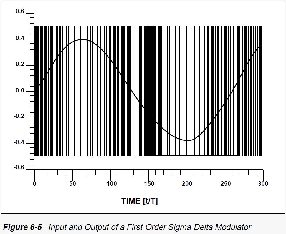
4 As the analog input signal increases in magnitude, so does the occurrence of 1's in the digital output of the flipflop: A parallel binary number output is obtained from this circuit by averaging the serial stream of bits together. For example, a counter circuit could be designed to collect the total number of 1's output by the flip-flop in a given number of clock pulses. This count would then be indicative of the analog input voltage. Variations on this theme exist, employing multiple integrator stages and/or comparator circuits outputting more than 1 bit, but one concept common to all Σ converters is that of oversampling. Oversampling is when multiple samples of an analog signal are taken by an ADC (in this case, a 1-bit ADC), and those digitized samples are averaged. The end result is an effective increase in the number of bits resolved from the signal. In other words, an oversampled 1-bit ADC can do the same job as an 8-bit ADC with one-time sampling, albeit at a slower rate.
5
B. Sc. III Semester (Electronics) - ( ) Digital Electronics-II) BE-301 MODEL ANSWER (AS-2791)
 - ( ) Digital Electronics-II) BE-301 MODEL ANSWER (AS-2791)") B. Sc. III Semester (Electronics) - (2013-14) Digital Electronics-II) BE-301 MODEL ANSWER (AS-2791) Section-[A] i. (B) ii. (A) iii. (D) iv. (C) v. (C) vi. (C) vii. (D) viii. (B) Ans-(ix): In JK flip flop
B. Sc. III Semester (Electronics) - (2013-14) Digital Electronics-II) BE-301 MODEL ANSWER (AS-2791) Section-[A] i. (B) ii. (A) iii. (D) iv. (C) v. (C) vi. (C) vii. (D) viii. (B) Ans-(ix): In JK flip flop
Counter dan Register
 Counter dan Register Introduction Circuits for counting events are frequently used in computers and other digital systems. Since a counter circuit must remember its past states, it has to possess memory.
Name Of The Experiment: Sequential circuit design Latch, Flip-flop and Registers
 EEE 304 Experiment No. 07 Name Of The Experiment: Sequential circuit design Latch, Flip-flop and Registers Important: Submit your Prelab at the beginning of the lab. Prelab 1: Construct a S-R Latch and
Asynchronous (Ripple) Counters
 Counters") Circuits for counting events are frequently used in computers and other digital systems. Since a counter circuit must remember its past states, it has to possess memory. The chapter about flip-flops introduced
Circuits for counting events are frequently used in computers and other digital systems. Since a counter circuit must remember its past states, it has to possess memory. The chapter about flip-flops introduced
Computer Organization & Architecture Lecture #5
 Computer Organization & Architecture Lecture #5 Shift Register A shift register is a register in which binary data can be stored and then shifted left or right when a shift signal is applied. Bits shifted
RS flip-flop using NOR gate
 RS flip-flop using NOR gate Triggering and triggering methods Triggering : Applying train of pulses, to set or reset the memory cell is known as Triggering. Triggering methods:- There are basically two
Introduction. Serial In - Serial Out Shift Registers (SISO)
") Introduction Shift registers are a type of sequential logic circuit, mainly for storage of digital data. They are a group of flip-flops connected in a chain so that the output from one flip-flop becomes
Introduction Shift registers are a type of sequential logic circuit, mainly for storage of digital data. They are a group of flip-flops connected in a chain so that the output from one flip-flop becomes
Logic Design II (17.342) Spring Lecture Outline
 Spring Lecture Outline") Logic Design II (17.342) Spring 2012 Lecture Outline Class # 03 February 09, 2012 Dohn Bowden 1 Today s Lecture Registers and Counters Chapter 12 2 Course Admin 3 Administrative Admin for tonight Syllabus
Logic Design II (17.342) Spring 2012 Lecture Outline Class # 03 February 09, 2012 Dohn Bowden 1 Today s Lecture Registers and Counters Chapter 12 2 Course Admin 3 Administrative Admin for tonight Syllabus
16 Stage Bi-Directional LED Sequencer
 16 Stage Bi-Directional LED Sequencer The bi-directional sequencer uses a 4 bit binary up/down counter (CD4516) and two "1 of 8 line decoders" (74HC138 or 74HCT138) to generate the popular "Night Rider"
Digital Circuits I and II Nov. 17, 1999
 Physics 623 Digital Circuits I and II Nov. 17, 1999 Digital Circuits I 1 Purpose To introduce the basic principles of digital circuitry. To understand the small signal response of various gates and circuits
COMP sequential logic 1 Jan. 25, 2016
 OMP 273 5 - sequential logic 1 Jan. 25, 2016 Sequential ircuits All of the circuits that I have discussed up to now are combinational digital circuits. For these circuits, each output is a logical combination
Computer Systems Architecture
 Computer Systems Architecture Fundamentals Of Digital Logic 1 Our Goal Understand Fundamentals and basics Concepts How computers work at the lowest level Avoid whenever possible Complexity Implementation
Introduction to Microprocessor & Digital Logic
 ME262 Introduction to Microprocessor & Digital Logic (Sequential Logic) Summer 2 Sequential Logic Definition The output(s) of a sequential circuit depends d on the current and past states of the inputs,
BISHOP ANSTEY HIGH SCHOOL & TRINITY COLLEGE EAST SIXTH FORM CXC CAPE PHYSICS, UNIT 2 Ms. S. S. CALBIO NOTES lesson #39
 BISHOP ANSTEY HIGH SCHOOL & TRINITY COLLEGE EAST SIXTH FORM CXC CAPE PHYSICS, UNIT 2 Ms. S. S. CALBIO NOTES lesson #39 Objectives: Students should be able to Thursday 21 st January 2016 @ 10:45 am Module
ECE 172 Digital Systems. Chapter 2.2 Review: Ring Counter, Johnson Counter. Herbert G. Mayer, PSU Status 7/14/2018
 ECE 172 Digital Systems Chapter 2.2 Review: Ring Counter, Johnson Counter Herbert G. Mayer, PSU Status 7/14/2018 1 Syllabus l Ring Counter l Parallel Output Ring Counter l Ring Counter via D Flip-Flops
RS flip-flop using NOR gate
 RS flip-flop using NOR gate Triggering and triggering methods Triggering : Applying train of pulses, to set or reset the memory cell is known as Triggering. Triggering methods:- There are basically two
Logic Design. Flip Flops, Registers and Counters
 Logic Design Flip Flops, Registers and Counters Introduction Combinational circuits: value of each output depends only on the values of inputs Sequential Circuits: values of outputs depend on inputs and
MAHARASHTRA STATE BOARD OF TECHNICAL EDUCATION (Autonomous) (ISO/IEC Certified) WINTER 2018 EXAMINATION MODEL ANSWER
 (ISO/IEC Certified) WINTER 2018 EXAMINATION MODEL ANSWER") Important Instructions to examiners: 1) The answers should be examined by key words and not as word-to-word as given in themodel answer scheme. 2) The model answer and the answer written by candidate may
Important Instructions to examiners: 1) The answers should be examined by key words and not as word-to-word as given in themodel answer scheme. 2) The model answer and the answer written by candidate may
Flip Flop. S-R Flip Flop. Sequential Circuits. Block diagram. Prepared by:- Anwar Bari
 Sequential Circuits The combinational circuit does not use any memory. Hence the previous state of input does not have any effect on the present state of the circuit. But sequential circuit has memory
DEPARTMENT OF ELECTRICAL &ELECTRONICS ENGINEERING DIGITAL DESIGN
 DEPARTMENT OF ELECTRICAL &ELECTRONICS ENGINEERING DIGITAL DESIGN Assoc. Prof. Dr. Burak Kelleci Spring 2018 OUTLINE Synchronous Logic Circuits Latch Flip-Flop Timing Counters Shift Register Synchronous
Analogue Versus Digital [5 M]
![Analogue Versus Digital [5 M]](/thumbs/93/111640168.jpg "Analogue Versus Digital [5 M]") Q.1 a. Analogue Versus Digital [5 M] There are two basic ways of representing the numerical values of the various physical quantities with which we constantly deal in our day-to-day lives. One of the ways,
Q.1 a. Analogue Versus Digital [5 M] There are two basic ways of representing the numerical values of the various physical quantities with which we constantly deal in our day-to-day lives. One of the ways,
CSC Computer Architecture and Organization
 S 37 - omputer Architecture and Organization Lecture 6: Registers and ounters Registers A register is a group of flip-flops. Each flip-flop stores one bit of data; n flip-flops are required to store n
INC 253 Digital and electronics laboratory I
 INC 253 Digital and electronics laboratory I Laboratory 9 Sequential Circuit Author: ID Co-Authors: 1. ID 2. ID 3. ID Experiment Date: Report received Date: Comments For Instructor Full Marks Pre lab 10
Logic Design II (17.342) Spring Lecture Outline
 Spring Lecture Outline") Logic Design II (17.342) Spring 2012 Lecture Outline Class # 05 February 23, 2012 Dohn Bowden 1 Today s Lecture Analysis of Clocked Sequential Circuits Chapter 13 2 Course Admin 3 Administrative Admin
Logic Design II (17.342) Spring 2012 Lecture Outline Class # 05 February 23, 2012 Dohn Bowden 1 Today s Lecture Analysis of Clocked Sequential Circuits Chapter 13 2 Course Admin 3 Administrative Admin
Sequential Logic Notes
 Sequential Logic Notes Andrew H. Fagg igital logic circuits composed of components such as AN, OR and NOT gates and that do not contain loops are what we refer to as stateless. In other words, the output
Sri Vidya College of Engineering And Technology. Virudhunagar Department of Electrical and Electronics Engineering
 Sri Vidya College of Engineering And Technology Virudhunagar 626 005 Department of Electrical and Electronics Engineering Year/ Semester/ Class : II/ III/ EEE Academic Year: 2017-2018 Subject Code/ Name:
Advanced Devices. Registers Counters Multiplexers Decoders Adders. CSC258 Lecture Slides Steve Engels, 2006 Slide 1 of 20
 Advanced Devices Using a combination of gates and flip-flops, we can construct more sophisticated logical devices. These devices, while more complex, are still considered fundamental to basic logic design.
L5 Sequential Circuit Design
 L Sequential Circuit Design Sequential Circuit Design Mealy and Moore Characteristic Equations Design Procedure Example Sequential Problem from specification to implementation Ref: Unit 14 of text 9/2/2012
Lecture 8: Sequential Logic
 Lecture 8: Sequential Logic Last lecture discussed how we can use digital electronics to do combinatorial logic we designed circuits that gave an immediate output when presented with a given set of inputs
Modified Sigma-Delta Converter and Flip-Flop Circuits Used for Capacitance Measuring
 Modified Sigma-Delta Converter and Flip-Flop Circuits Used for Capacitance Measuring MILAN STORK Department of Applied Electronics and Telecommunications University of West Bohemia P.O. Box 314, 30614
Introduction. NAND Gate Latch. Digital Logic Design 1 FLIP-FLOP. Digital Logic Design 1
 2007 Introduction BK TP.HCM FLIP-FLOP So far we have seen Combinational Logic The output(s) depends only on the current values of the input variables Here we will look at Sequential Logic circuits The
Find the equivalent decimal value for the given value Other number system to decimal ( Sample)
") VELAMMAL COLLEGE OF ENGINEERING AND TECHNOLOGY, MADURAI 65 009 Department of Information Technology Model Exam-II-Question bank PART A (Answer for all Questions) (8 X = 6) K CO Marks Find the equivalent
VELAMMAL COLLEGE OF ENGINEERING AND TECHNOLOGY, MADURAI 65 009 Department of Information Technology Model Exam-II-Question bank PART A (Answer for all Questions) (8 X = 6) K CO Marks Find the equivalent
4.S-[F] SU-02 June All Syllabus Science Faculty B.Sc. II Yr. Instrumentation Practice [Sem.III & IV] S.Lot
![4.S-[F] SU-02 June All Syllabus Science Faculty B.Sc. II Yr. Instrumentation Practice [Sem.III & IV] S.Lot](/thumbs/90/103282534.jpg "4.S-[F] SU-02 June All Syllabus Science Faculty B.Sc. II Yr. Instrumentation Practice [Sem.III & IV] S.Lot") [Sem.III & IV] S.Lot. - 1 - [Sem.III & IV] S.Lot. - 2 - [Sem.III & IV] S.Lot. - 3 - Syllabus B.Sc. ( Instrumentation Practice ) Second Year ( Third and Forth Semester ) ( Effective from June 2014 ) [Sem.III
[Sem.III & IV] S.Lot. - 1 - [Sem.III & IV] S.Lot. - 2 - [Sem.III & IV] S.Lot. - 3 - Syllabus B.Sc. ( Instrumentation Practice ) Second Year ( Third and Forth Semester ) ( Effective from June 2014 ) [Sem.III
Lecture 12. Amirali Baniasadi
 CENG 24 Digital Design Lecture 2 Amirali Baniasadi amirali@ece.uvic.ca This Lecture Chapter 6: Registers and Counters 2 Registers Sequential circuits are classified based in their function, e.g., registers.
UNIT IV. Sequential circuit
 UNIT IV Sequential circuit Introduction In the previous session, we said that the output of a combinational circuit depends solely upon the input. The implication is that combinational circuits have no
LSN 12 Shift Registers
 LSN 12 Shift Registers Department of Engineering Technology LSN 12 Shift Registers Digital circuits with data storage and data movement functions Storage capacity is the total number of bits of digital
Rangkaian Sekuensial. Flip-flop
 Rangkaian Sekuensial Rangkaian Sekuensial Flip-flop Combinational versus Sequential Functions Logic functions are categorized as being either combinational (sometimes referred to as combinatorial) or sequential.
Chapter 6. Flip-Flops and Simple Flip-Flop Applications
 Chapter 6 Flip-Flops and Simple Flip-Flop Applications Basic bistable element It is a circuit having two stable conditions (states). It can be used to store binary symbols. J. C. Huang, 2004 Digital Logic
Sequential Digital Design. Laboratory Manual. Experiment #7. Counters
 The Islamic University of Gaza Engineering Faculty Department of Computer Engineering Spring 2018 ECOM 2022 Khaleel I. Shaheen Sequential Digital Design Laboratory Manual Experiment #7 Counters Objectives
Chapter 5 Flip-Flops and Related Devices
 Chapter 5 Flip-Flops and Related Devices Chapter 5 Objectives Selected areas covered in this chapter: Constructing/analyzing operation of latch flip-flops made from NAND or NOR gates. Differences of synchronous/asynchronous
Slide 1. Flip-Flops. Cross-NOR SR flip-flop S R Q Q. hold reset set not used. Cross-NAND SR flip-flop S R Q Q. not used reset set hold 1 Q.
 Slide Flip-Flops Cross-NOR SR flip-flop Reset Set Cross-NAND SR flip-flop Reset Set S R reset set not used S R not used reset set 6.7 Digital ogic Slide 2 Clocked evel-triggered NAND SR Flip-Flop S R SR
Digital Logic Design ENEE x. Lecture 19
 Digital Logic Design ENEE 244-010x Lecture 19 Announcements Homework 8 due on Monday, 11/23. Agenda Last time: Timing Considerations (6.3) Master-Slave Flip-Flops (6.4) This time: Edge-Triggered Flip-Flops
DIGITAL ELECTRONICS MCQs
 DIGITAL ELECTRONICS MCQs 1. A 8-bit serial in / parallel out shift register contains the value 8, clock signal(s) will be required to shift the value completely out of the register. A. 1 B. 2 C. 4 D. 8
CSE Latches and Flip-flops Dr. Izadi. NOR gate property: A B Z Cross coupled NOR gates: S M S R Q M
 CSE-4523 Latches and Flip-flops Dr. Izadi NOR gate property: A B Z A B Z Cross coupled NOR gates: S M S R M R S M R S R S R M S S M R R S ' Gate R Gate S R S G R S R (t+) S G R Flip_flops:. S-R flip-flop
Vignana Bharathi Institute of Technology UNIT 4 DLD
 DLD UNIT IV Synchronous Sequential Circuits, Latches, Flip-flops, analysis of clocked sequential circuits, Registers, Shift registers, Ripple counters, Synchronous counters, other counters. Asynchronous
Note 5. Digital Electronic Devices
 Note 5 Digital Electronic Devices Department of Mechanical Engineering, University Of Saskatchewan, 57 Campus Drive, Saskatoon, SK S7N 5A9, Canada 1 1. Binary and Hexadecimal Numbers Digital systems perform
DALHOUSIE UNIVERSITY Department of Electrical & Computer Engineering Digital Circuits - ECED 220. Experiment 4 - Latches and Flip-Flops
 DLHOUSIE UNIVERSITY Department of Electrical & Computer Engineering Digital Circuits - ECED 0 Experiment - Latches and Flip-Flops Objectives:. To implement an RS latch memory element. To implement a JK
YEDITEPE UNIVERSITY DEPARTMENT OF COMPUTER ENGINEERING. EXPERIMENT VIII: FLIP-FLOPS, COUNTERS 2014 Fall
 YEDITEPE UNIVERSITY DEPARTMENT OF COMPUTER ENGINEERING EXPERIMENT VIII: FLIP-FLOPS, COUNTERS 2014 Fall Objective: - Dealing with the operation of simple sequential devices. Learning invalid condition in
SEQUENTIAL LOGIC. Satish Chandra Assistant Professor Department of Physics P P N College, Kanpur
 SEQUENTIAL LOGIC Satish Chandra Assistant Professor Department of Physics P P N College, Kanpur www.satish0402.weebly.com OSCILLATORS Oscillators is an amplifier which derives its input from output. Oscillators
WINTER 14 EXAMINATION
 Subject Code: 17320 WINTER 14 EXAMINATION Model Answer Important Instructions to examiners: 1) The answers should be examined by key words and not as word-to-word as given in the model answer scheme. 2)
Chapter 4: One-Shots, Counters, and Clocks
 Chapter 4: One-Shots, Counters, and Clocks I. The Monostable Multivibrator (One-Shot) The timing pulse is one of the most common elements of laboratory electronics. Pulses can control logical sequences
MAHARASHTRA STATE BOARD OF TECHNICAL EDUCATION (Autonomous) (ISO/IEC Certified)
 (ISO/IEC Certified)") Important Instructions to examiners: 1) The answers should be examined by key words and not as word-to-word as given in the model answer scheme. 2) The model answer and the answer written by candidate
Important Instructions to examiners: 1) The answers should be examined by key words and not as word-to-word as given in the model answer scheme. 2) The model answer and the answer written by candidate
(Refer Slide Time: 2:00)
") Digital Circuits and Systems Prof. Dr. S. Srinivasan Department of Electrical Engineering Indian Institute of Technology, Madras Lecture #21 Shift Registers (Refer Slide Time: 2:00) We were discussing
Digital Circuits and Systems Prof. Dr. S. Srinivasan Department of Electrical Engineering Indian Institute of Technology, Madras Lecture #21 Shift Registers (Refer Slide Time: 2:00) We were discussing
Final Exam review: chapter 4 and 5. Supplement 3 and 4
 Final Exam review: chapter 4 and 5. Supplement 3 and 4 1. A new type of synchronous flip-flop has the following characteristic table. Find the corresponding excitation table with don t cares used as much
D Latch (Transparent Latch)
") D Latch (Transparent Latch) -One way to eliminate the undesirable condition of the indeterminate state in the SR latch is to ensure that inputs S and R are never equal to 1 at the same time. This is done
D Latch (Transparent Latch) -One way to eliminate the undesirable condition of the indeterminate state in the SR latch is to ensure that inputs S and R are never equal to 1 at the same time. This is done
Logic Design Viva Question Bank Compiled By Channveer Patil
 Logic Design Viva Question Bank Compiled By Channveer Patil Title of the Practical: Verify the truth table of logic gates AND, OR, NOT, NAND and NOR gates/ Design Basic Gates Using NAND/NOR gates. Q.1
(Refer Slide Time: 2:05)
") (Refer Slide Time: 2:05) Digital Circuits and Systems Prof. S. Srinivasan Department of Electrical Engineering Indian Institute of Technology, Madras Triggering Mechanisms of Flip Flops and Counters Lecture
(Refer Slide Time: 2:05) Digital Circuits and Systems Prof. S. Srinivasan Department of Electrical Engineering Indian Institute of Technology, Madras Triggering Mechanisms of Flip Flops and Counters Lecture
Synchronous Sequential Logic
 Synchronous Sequential Logic -A Sequential Circuit consists of a combinational circuit to which storage elements are connected to form a feedback path. The storage elements are devices capable of storing
The outputs are formed by a combinational logic function of the inputs to the circuit or the values stored in the flip-flops (or both).
.") 1 The outputs are formed by a combinational logic function of the inputs to the circuit or the values stored in the flip-flops (or both). The value that is stored in a flip-flop when the clock pulse occurs
1 The outputs are formed by a combinational logic function of the inputs to the circuit or the values stored in the flip-flops (or both). The value that is stored in a flip-flop when the clock pulse occurs
Dual Slope ADC Design from Power, Speed and Area Perspectives
 Dual Slope ADC Design from Power, Speed and Area Perspectives Isaac Macwan, Xingguo Xiong, Lawrence Hmurcik Department of Electrical & Computer Engineering, University of Bridgeport, Bridgeport, CT 06604
Chapter 6 Digital Circuit 6-5 Department of Mechanical Engineering
 MEMS1082 Chapter 6 Digital Circuit 6-5 General digital system D Flip-Flops, The D flip-flop is a modification of the clocked SR flip-flop. The D input goes directly into the S input and the complement
(CSC-3501) Lecture 7 (07 Feb 2008) Seung-Jong Park (Jay) CSC S.J. Park. Announcement
 Lecture 7 (07 Feb 2008) Seung-Jong Park (Jay) CSC S.J. Park. Announcement") Seung-Jong Park (Jay) http://www.csc.lsu.edu/~sjpark Computer Architecture (CSC-3501) Lecture 7 (07 Feb 2008) 1 Announcement 2 1 Combinational vs. Sequential Logic Combinational Logic Memoryless Outputs
Seung-Jong Park (Jay) http://www.csc.lsu.edu/~sjpark Computer Architecture (CSC-3501) Lecture 7 (07 Feb 2008) 1 Announcement 2 1 Combinational vs. Sequential Logic Combinational Logic Memoryless Outputs
MAHARASHTRA STATE BOARD OF TECHNICAL EDUCATION (Autonomous)
") Subject Code: 17320 Model Answer Page 1 of 32 Important Instructions to examiners: 1) The answers should be examined by key words and not as word-to-word as given in the Model answer scheme. 2) The model
Subject Code: 17320 Model Answer Page 1 of 32 Important Instructions to examiners: 1) The answers should be examined by key words and not as word-to-word as given in the Model answer scheme. 2) The model
Logic. Andrew Mark Allen March 4, 2012
 Logic Andrew Mark Allen - 05370299 March 4, 2012 Abstract NAND gates and inverters were used to construct several different logic gates whose operations were investigate under various inputs. Then the
1. Convert the decimal number to binary, octal, and hexadecimal.
 1. Convert the decimal number 435.64 to binary, octal, and hexadecimal. 2. Part A. Convert the circuit below into NAND gates. Insert or remove inverters as necessary. Part B. What is the propagation delay
Interfacing Analog to Digital Data Converters. A/D D/A Converter 1
 Interfacing Analog to Digital Data Converters A/D D/A Converter 1 In most of the cases, the PPI 8255 is used for interfacing the analog to digital converters with microprocessor. The analog to digital
Sequential Logic and Clocked Circuits
 Sequential Logic and Clocked Circuits Clock or Timing Device Input Variables State or Memory Element Combinational Logic Elements From combinational logic, we move on to sequential logic. Sequential logic
Serial In/Serial Left/Serial Out Operation
 Shift Registers The need to storage binary data was discussed earlier. In digital circuits multi-bit data has to be stored temporarily until it is processed. A flip-flop is able to store a single binary
Module -5 Sequential Logic Design
 Module -5 Sequential Logic Design 5.1. Motivation: In digital circuit theory, sequential logic is a type of logic circuit whose output depends not only on the present value of its input signals but on
MODU LE DAY. Class-A, B, AB and C amplifiers - basic concepts, power, efficiency Basic concepts of Feedback and Oscillation. Day 1
 DAY MODU LE TOPIC QUESTIONS Day 1 Day 2 Day 3 Day 4 I Class-A, B, AB and C amplifiers - basic concepts, power, efficiency Basic concepts of Feedback and Oscillation Phase Shift Wein Bridge oscillators.
Part 4: Introduction to Sequential Logic. Basic Sequential structure. Positive-edge-triggered D flip-flop. Flip-flops classified by inputs
 Part 4: Introduction to Sequential Logic Basic Sequential structure There are two kinds of components in a sequential circuit: () combinational blocks (2) storage elements Combinational blocks provide
Dr. Shahram Shirani COE2DI4 Midterm Test #2 Nov 19, 2008
 Page 1 Dr. Shahram Shirani COE2DI4 Midterm Test #2 Nov 19, 2008 Instructions: This examination paper includes 13 pages and 20 multiple-choice questions starting on page 3. You are responsible for ensuring
FLIP-FLOPS AND RELATED DEVICES
 C H A P T E R 5 FLIP-FLOPS AND RELATED DEVICES OUTLINE 5- NAND Gate Latch 5-2 NOR Gate Latch 5-3 Troubleshooting Case Study 5-4 Digital Pulses 5-5 Clock Signals and Clocked Flip-Flops 5-6 Clocked S-R Flip-Flop
Decade Counters Mod-5 counter: Decade Counter:
 Decade Counters We can design a decade counter using cascade of mod-5 and mod-2 counters. Mod-2 counter is just a single flip-flop with the two stable states as 0 and 1. Mod-5 counter: A typical mod-5
Universal Asynchronous Receiver- Transmitter (UART)
") Universal Asynchronous Receiver- Transmitter (UART) (UART) Block Diagram Four-Bit Bidirectional Shift Register Shift Register Counters Shift registers can form useful counters by recirculating a pattern
Universal Asynchronous Receiver- Transmitter (UART) (UART) Block Diagram Four-Bit Bidirectional Shift Register Shift Register Counters Shift registers can form useful counters by recirculating a pattern
TYPICAL QUESTIONS & ANSWERS
 DIGITALS ELECTRONICS TYPICAL QUESTIONS & ANSWERS OBJECTIVE TYPE QUESTIONS Each Question carries 2 marks. Choose correct or the best alternative in the following: Q.1 The NAND gate output will be low if
Sequential Logic. Analysis and Synthesis. Joseph Cavahagh Santa Clara University. r & Francis. TaylonSi Francis Group. , Boca.Raton London New York \
 Sequential Logic Analysis and Synthesis Joseph Cavahagh Santa Clara University r & Francis TaylonSi Francis Group, Boca.Raton London New York \ CRC is an imprint of the Taylor & Francis Group, an informa
EKT 121/4 ELEKTRONIK DIGIT 1
 EKT 121/4 ELEKTRONIK DIGIT 1 Kolej Universiti Kejuruteraan Utara Malaysia Bistable Storage Devices and Related Devices Introduction Latches and flip-flops are the basic single-bit memory elements used
Computer Science 324 Computer Architecture Mount Holyoke College Fall Topic Notes: Sequential Circuits
 Computer Science 324 Computer Architecture Mount Holyoke College Fall 2007 opic Notes: Sequential Circuits Let s think about how life can be bad for a circuit. Edge Detection Consider this one: What is
EXPERIMENT #6 DIGITAL BASICS
 EXPERIMENT #6 DIGITL SICS Digital electronics is based on the binary number system. Instead of having signals which can vary continuously as in analog circuits, digital signals are characterized by only
MODEL QUESTIONS WITH ANSWERS THIRD SEMESTER B.TECH DEGREE EXAMINATION DECEMBER CS 203: Switching Theory and Logic Design. Time: 3 Hrs Marks: 100
 MODEL QUESTIONS WITH ANSWERS THIRD SEMESTER B.TECH DEGREE EXAMINATION DECEMBER 2016 CS 203: Switching Theory and Logic Design Time: 3 Hrs Marks: 100 PART A ( Answer All Questions Each carries 3 Marks )
Application Note. A Collection of Application Hints for the CS501X Series of A/D Converters. By Jerome Johnston
 AN08 Application Note A Collection of Application Hints for the CS501X Series of A/D Converters By Jerome Johnston Jam ADC into Coarse Charge for High Slew Signals Single Control Input Acts as a "Start
AC103/AT103 ANALOG & DIGITAL ELECTRONICS JUN 2015
 Q.2 a. Draw and explain the V-I characteristics (forward and reverse biasing) of a pn junction. (8) Please refer Page No 14-17 I.J.Nagrath Electronic Devices and Circuits 5th Edition. b. Draw and explain
Converters: Analogue to Digital
 Converters: Analogue to Digital Presented by: Dr. Walid Ghoneim References: Process Control Instrumentation Technology, Curtis Johnson Op Amps Design, Operation and Troubleshooting. David Terrell 1 - ADC
TRAINING KITS ON DIGITAL ELECTRONIC EXPERIMENTS. Verify Truth table for TTL IC s AND, NOT, & NAND GATES
 TRAINING KITS ON DIGITAL ELECTRONIC EXPERIMENTS CEE 2800 Basic Logic Gates using TTL IC's (7 in 1) To verify the truth table For TTL AND, OR. NOT, NAND,NOR, EX-OR, & EX-NOR Gates. Instrument comprises
Counters
 Counters A counter is the most versatile and useful subsystems in the digital system. A counter driven by a clock can be used to count the number of clock cycles. Since clock pulses occur at known intervals,
EE292: Fundamentals of ECE
 EE292: Fundamentals of ECE Fall 2012 TTh 10:00-11:15 SEB 1242 Lecture 23 121120 http://www.ee.unlv.edu/~b1morris/ee292/ 2 Outline Review Combinatorial Logic Sequential Logic 3 Combinatorial Logic Circuits
CCE RR REVISED & UN-REVISED KARNATAKA SECONDARY EDUCATION EXAMINATION BOARD, MALLESWARAM, BANGALORE G È.G È.G È..
 CCE RR REVISED & UN-REVISED O %lo ÆË v ÃO y Æ fio» flms ÿ,» fl Ê«fiÀ M, ÊMV fl 560 003 KARNATAKA SECONDARY EDUCATION EXAMINATION BOARD, MALLESWARAM, BANGALORE 560 003 G È.G È.G È.. Æ fioê, d È 2018 S.
EECS 270 Midterm Exam Spring 2011
 EES 270 Midterm Exam Spring 2011 Name: unique name: Sign the honor code: I have neither given nor received aid on this exam nor observed anyone else doing so. Scores: Page # Points 2 /15 3 /10 4 /6 5 /12
University of Pennsylvania Department of Electrical and Systems Engineering. Digital Design Laboratory. Lab8 Calculator
 University of Pennsylvania Department of Electrical and Systems Engineering Digital Design Laboratory Purpose Lab Calculator The purpose of this lab is: 1. To get familiar with the use of shift registers
ASYNCHRONOUS COUNTER CIRCUITS
 ASYNCHRONOUS COUNTER CIRCUITS Asynchronous counters do not have a common clock that controls all the Hipflop stages. The control clock is input into the first stage, or the LSB stage of the counter. The
Unit-5 Sequential Circuits - 1
 Unit-5 Sequential Circuits - 1 1. With the help of block diagram, explain the working of a JK Master-Slave flip flop. 2. Differentiate between combinational circuit and sequential circuit. 3. Explain Schmitt
THE KENYA POLYTECHNIC
 THE KENYA POLYTECHNIC ELECTRICAL/ELECTRONICS ENGINEERING DEPARTMENT HIGHER DIPLOMA IN ELECTRICAL ENGINEERING END OF YEAR II EXAMINATIONS NOVEMBER 006 DIGITAL ELECTRONICS 3 HOURS INSTRUCTIONS TO CANDIDATES:
Software Engineering 2DA4. Slides 9: Asynchronous Sequential Circuits
 Software Engineering 2DA4 Slides 9: Asynchronous Sequential Circuits Dr. Ryan Leduc Department of Computing and Software McMaster University Material based on S. Brown and Z. Vranesic, Fundamentals of
A MISSILE INSTRUMENTATION ENCODER
 A MISSILE INSTRUMENTATION ENCODER Item Type text; Proceedings Authors CONN, RAYMOND; BREEDLOVE, PHILLIP Publisher International Foundation for Telemetering Journal International Telemetering Conference
Computer Science 324 Computer Architecture Mount Holyoke College Fall Topic Notes: Sequential Circuits
 Computer Science 324 Computer Architecture Mount Holyoke College Fall 2009 opic Notes: Sequential Circuits Let s think about how life can be bad for a circuit. Edge Detection Consider this one: What is
CHAPTER1: Digital Logic Circuits
 CS224: Computer Organization S.KHABET CHAPTER1: Digital Logic Circuits 1 Sequential Circuits Introduction Composed of a combinational circuit to which the memory elements are connected to form a feedback
Unit 11. Latches and Flip-Flops
 Unit 11 Latches and Flip-Flops 1 Combinational Circuits A combinational circuit consists of logic gates whose outputs, at any time, are determined by combining the values of the inputs. For n input variables,
MUHAMMAD NAEEM LATIF MCS 3 RD SEMESTER KHANEWAL
 1. A stage in a shift register consists of (a) a latch (b) a flip-flop (c) a byte of storage (d) from bits of storage 2. To serially shift a byte of data into a shift register, there must be (a) one click
Saturated Non Saturated PMOS NMOS CMOS RTL Schottky TTL ECL DTL I I L TTL
 EC6302-DIGITAL ELECTRONICS UNIT I MINIMIZATION TECHNIQUES AND LOGIC GATES 1. Define binary logic? Binary logic consists of binary variables and logical operations. The variables are designated by the alphabets