The transition from understanding the operation of a simple adder, built during a sixth-form science session, to understanding how a full sized
|
|
|
- John Bates
- 6 years ago
- Views:
Transcription
1
2
3 The transition from understanding the operation of a simple adder, built during a sixth-form science session, to understanding how a full sized digital computer can through-put vast amounts of scientific or business information, is a difficult one. Even if a school possesses a computer a student, who has been taught the essentials of programming and can operate the machine, may find it difficult to understand, from an electronic point of view, how the computer handles the numbers he feeds into it. The problem arises in the difference in scale between laboratory practical work and the complexity of a modern computer. The Wireless World digital computer was designed as a stepping stone between these two extremes to demonstrate how electronic circuits can manipulate and store numbers and to give an idea of how computer systems are organized. An analysis of the correspondence arising from the series of articles describing the computer (published in the August to December 1967 issues of Wireless World), rather gratifyingly did not show any set pattern, implying that no two groups of constructors encountered the same problems. However, a number of readers complained at the apparent " maximization " of the design. Many readers will know that a particular Boolean expression can be formed with a large number of different combinations of logic elements and that one of these combinations uses the least number of elements; this is known as the minimal form. Minimization is carried out using a mixture of experience and Boolean manipulation. Once a circuit has been minimized the way in which it operates usually becomes obscured. The Wireless World computer has been deliberately kept in a " maximal " form so that its operation can be easily visualized and understood. Construction of the computer has been undertaken by a number of schools who have found that the project has encouraged class discussions on the problems associated with constructing the machine and the design of this and other computers resulting in a clearer understanding of what digital computing is all about.

4 WIRELESS WORLD DIGITAL COMPUTER Outline description: basic theory: circuit elements Low-cost desk-top binary machine for small-scale calculations and for use in schools as a teaching aid, designed by B. Crank of " Wirless World" staff. Numbers are fed in manually and results of calculations are read from indicator lamps. Instructions, entered in binary coded form by a set of switches, are interpreted and carried out automatically by the machine. THE Wireless World Digital Computer has been designed as a low cost system capable of demonstrating basic computer methods and various operations in the binary number system. It will add, subtract, multiply and divide eight-bit binary numbers, which are entered manually by means of press switches. It will also complement a binary number, and this feature makes possible arithmetic operations with mixed positive and negative numbers and subtraction using the Is and 2s complement methods. The machine can be programmed to convert natural binary numbers into natural binary coded decimal form, making the job of interpreting results easier. The largest number that can be accommodated by the computer is the maximum obtainable with eight binary digits, which is 255. Results of calculations and the states of all major circuits are indicated on the front panel by small neon lamps. This means that each computer operation can be analysed in detail and fault diagnosis is made easier. Instructions to the computer to perform required operations are entered, in numerical code form, by means of a set of eight switches, and the machine interprets the code and carries out the instructions automatically. A choice of three operating speeds is provided. These are: "one bit," in which the start button is used to initiate separately each operation at each successive binary position; " slow," in which pressing the start button causes a complete arithmetical operation (e.g. adding two 8-digit numbers) to be performed at the rate of about 2 binary positions per second; and " normal " which is similar in principle to " slow " but at the higher speed of 2,500 positions per second. In its present form the computer will carry out one instruction a complete arithmetical operation at a time. With the addition of a few extra parts a whole sequence of instructions could be carried out automatically, enabling basic programming to be taught. A simplified block schematic diagram of the computer is shown in Fig. 1. Numerical data are fed straight into the arithmetic unit by the data input unit and are operated on by the computer in a manner determined by the order register, at one of three speeds (mentioned above) selected by the demonstration switching. The order register is the means by which binary coded instructions to the computer to perform a particular operation are fed in and held. The order decoder translates the instruction presented to it by the order register into a form that the computer can " understand," and causes it to be carried out by routing pulses, generated in the control unit, to the correct sections of the computer. The exact number of pulses generated by the control unit will depend on what the decoder " tells " it to do and on the internal condition of the arithmetic unit. Data can be transferred from the arithmetic unit to the store for later use or from the store to the arithmetic unit. The condition of all circuits in the arithmetic unit and store are continuously monitored on the front panel by the readout section so that if desired any particular operation can be analysed in detail. The computer operates in the " serial " mode, which means that the binary information being transferred along the routes shown in Fig. 1 is represented by time sequences of electrical states. Thus when a number is being handled the digits in the successive binary positions are dealt with one after the other, starting with the least significant digit and working upwards. Fig. I. Simplified schematic showing principal units of the computer. WIRELESS WORLD, AUGUST 1967
5 An important factor in any project is cost and everything possible has been done to keep this within reasonable bounds. The prototype cost something in the region of 50-60, not including the cabinet. The transistors used are, for the most part, reject germanium types available for under Is each, the remainder being 60 V silicon types that can be bought for about 2s each. An attempt has been made to use resistors of the same value wherever possible so that price reductions can be obtained by quantity buying (say 2d each). The large quantity of diodes used cost about 4 d each. The main difficulty is in obtaining cheap capacitors, as prices range from about 9d to Is per item. However, if a systematic approach is made to this problem much more favourable prices can be obtained. The method adopted in the prototype was to ask various retailers for quotations for the quantities involved, in this manner a price of 4d per capacitor was achieved. Before construction of the computer is contemplated it is essential that the intending builder be thoroughly conversant with the theory involved (see " reminder " sections following). Accuracy in construction is equally important, for while trouble-shooting on the correctly built computer is not too difficult, locating faults when wiring errors are involved can be very trying. Stored-programme facility. Development work is being done on a sub-routine store for the computer. Early results are encouraging and should the store prove to be reliable it will be described in detail later. Basically it provides a further 64 words of storage (512 bits) that can hold either control words or data. Each word is stored by means of wired-in diodes or by diode " pegs " inserted into a matrix programming board. As the computer completes each operation the next instruction is automatically fed to the computer from the sub-routine store and is executed and this process continues until a " stop " instruction is received by the computer. In this way complete sequences of up to 64 separate instructions can be carried out automatically and basic programming can be taught and demonstrated. Continued on page 5 REMINDER ON BINARY ARITHMETIC Binary notation. In the binary system, only two characters are required for counting, and we shall use the conventional 0 and 1. As in the decimal system the digits have positional as well as numerical value as shown in the table (right). The values of digits in successive positions from right to left are increasing powers of two, 2, 2 1, 2 2, 2 :! (or 1, 2, 4, 8). Each binary digit is termed a " bit " and a complete binary number a " word." The weights of the digits in the eight-bit word used in our computer are therefore 2, 2 1, 2 2,2 3, 2 4, 2 5, 2, 2 7 (or 1, 2, 4, 8, 16, 32, 64, 128). To convert a binary number to a decimal number one can add the weights for each column in which a 1 appears. Consider the word 0110 (which from the table can be seen to equal decimal 6). The decimal number is obtained as follows: 0110 = (0 x 8) + (1 x 4) + (1 x 2) + (0 x 1) f = 6. A decimal number can be converted into a binary word by successive division by the weights to give successive quotients of Is and Os as follows: Convert decimal 163 to binary. 128) ) Reading the right hand column of quotients from top to bottom, this gives 163 = binary A number in the decimal system is based on powers of 10 and is said to have a radix of 10; similarly the binary system has a radix of 2. To indicate the radix being used, where necessary, the radix will be enclosed in brackets at the end of the number as is standard practice, i.e. 163< 10 ) = < 2 ) In addition to the pure or natural binary system discussed above, the natural binary coded decimal (n.b.c.d.) system is used in the computer. This uses four bits for each decimal place, these bits being the natural binary representation of each decimal digit, i.e. 163,,o) in n.b.c.d. is The instructions to the computer are given in another number system with a radix of 8 known as the octal code. The method used to convert a pure binary number to octal is similar to that for converting n.b.c.d. to decimal. The number is divided into groups of three digits starting from the right, then the decimal equivalent of each group is written down, as follows: 00/001/001 0/1/ (2) (8) Another example: 11/101/111 3/5/ ,2, (8 ) Because the computer uses only an eight-bit instruction word two bits appear in the left hand group, and therefore the maximum octal number that can appear in the left-hand place is 3. Binary arithmetic. This is best started by examining the following rules for adding two binary numbers: = = 0 carry 1 to next most significant position. Where the addition of two Is takes place, as there is no symbol to represent any number greater than 1, a carry to the nex t WIRELESS WORLD, AUGUST 1967
6 most significant position occurs. This is the same as saying = 2 1 or = Throughout this article, to indicate in a table that a carry has been generated the following symbolism will be used: >1 The next step is to add two four-bit binary numbers. The working is as follows: (positional values) From this it is seen that in order to add two binary numbers it is necessary to be able to add three digits to take into account any carry that may be generated during the previous addition. Another addition table is obviously called for: A B c = = »0 ->Q -*0-3»0 ->1 ->1 -»1 ->1 0 1 = 0 _ 0 1 = 1 Binary subtraction can be explained by a similar table. However, here a " borrow " can occur instead of the carry in addition. In the following table a borrow is indicated in the same way as a carry i.e. -> 1. A B C 0 0 with an borrow 0-^0 1 ->0 1 -> 0-> 1 -> 0-^ 1 -> As an example we will subtract 0 1 from 1 0, as follows: (positional values) 1 0 (minuend) ^_1_ (subtrahend) "0~T (difference) 1 (borrow) Starting with the right hand column > 1. In the left-hand column we have already borrowed a 1, so this has to be returned and we get: 1 0 with a 1 borrow Q > Q. Henceforward a borrow will be called a carry and an unnecessary term dispensed with. Multiplication can be performed by repeated addition (e.g. 8x4 = ) and division by repeated subtraction, e.g. 32 -: 8s [ ({(32 8) 8} 8 ) 8] 0. The quotient being obtained by counting the number of times subtraction was necessary to reduce 32 to 0, that is 4. Subtraction can be performed by use of the addition process, although our computer does not normally operate in this mode. The computer, however, will demonstrate the process, so an explanation is called for here. Two methods can be used, known as the Is complement method and the 2s complement method. First the Is complement method. Consider First, it is necessary to form the Is complement of the subtrahend This is done by changing all the Is to Os and all the Os to Is, to give To complete the subtraction we now add the two numbers and perform the " end around carry" operation: ; > 1 (end around carry) (sum, and result of subtraction) f~ We have used a four bit word and a carry is generated that exceeds our word length. This carry is added to the result of the first addition hence " end around carry". Thus In the 2s complement method, first the 2s complement of the subtrahend is formed. This is equal to the Is complement + 1. Using the previous example again ( ), the 2s complement of Then: 2* " i o i i but here the carry generated in the 2 4 position is ignored. Our computer forms the Is complement of a number by adding to it a series of Is and ignoring any carry that may be generated. Thus to form the Is complement of : _OJJ) I X (ignore carries) Other processes in binary arithmetic, such as operations with positive and negative numbers, will be discussed in the section dealing with programming the computer. REMINDER ON BOOLEAN SYMBOLS AND LOGIC ELEMENTS Boolean symbols do not represent quantities but logical states or conditions. For example, the symbols A andjj could represent two switches in the " on " position, while A and B could represent the same two switches in the " off" position. If these switches were connected in series with a battery and lamp, when both switches were " on " this condition would be symbolized as " A and B ", and it would result in the lamp being lit. If any other condition existed, i.e. A and B (A on, B off), or A and B (A off, B on) or A andl& (both off), the lamp would not light. This is a demonstration of the Boolean AND function the lamp is lit only when the condition A AND B obtains. If the condition of the lamp being lit is represented by the symbol C then it can be said that A and B = C or A. B = C or AB = C These three statements are identical; the two letters with a dot between, or close together, are shorthand for the AND function. The condition A is read as NOT A. Proceeding further with our two switches and lamp we can therefore say that where C (NOT C) indicates that the lamp is not lit. If the switches were connected in parallel then either switch being " on " would result in the lamp being lit. Here it is true to say that the condition " A or B " would result in C. The Boolean symbol for this function is +, which is read as OR. With the switches connected in parallel the following equations are true: A_+ B = C(AORB = C) AB =--= C (NOT A and NOT B = NOT C) In the above example A (NOT A) was represented by the absence of something (absence of conduction path), but it is important to remember that NOT A really means the presence WIRELESS WORLD, AUGUST 1967
7 of something other than A in fact its opposite state A. Thus A and A can be represented by any pair of denned electrical states: +6V and +2V, 0V and -4V and so on. Logic elements. The simplest of the circuits performing the above Boolean functions is the NOT gate. With this, for example, state A can be negated into A or vice versa, and the graphical symbol for such an element is shown in Fig. 2. If the input of this element goes_to earth the output will go to some voltage above earth. The 1 in the centre of the circle indicates that the element will negate one input, while the arrow shows the direction of information flow. The time has come to introduce one piece of terminology that will be used throughout the series of articles. The fact that a voltage exists at a particular point in a circuit can be represented by the terms " true ", " up ", 1 (binary), ve, + ve and so on, and the fact that a voltage does not exist can be represented by " false ", " down ", 0 (binary), 0V, etc. The use of Is and Os to define voltage levels has been rejected, as far as this series is concerned, for fear that they may become confused with binary Is and Os, i.e. numerical data. The term " up " will be used to indicate that a voltage is present and " down " to indicate that that line is at earth potential. An extension of the NOT gate is the NOR gate. Electronically they are almost identical but the NOR gate has more inputs, as shown by the symbol in Fig. 2. In the logic element used in the computer any input going " up " will result in the output going " down" and for the output to be " up" all inputs must be " down ". More or fewer inputs may be provided. Next in Fig. 2 is shown the symbol for an element performing the previously discussed OR function. In the practical OR GATE FORMED BY COMBINING NOR & NOT _AND GATE Fig. 2. Symbols for basic logic elements used in the computer. device any one of the inputs going " up " will result in the output going " up " as indicated by the " 1 " in the symbol, and the output will be " down" only when all the inputs are " down ". An OR gate can be formed by the combination of a NOR and a NOT gate as shown in Fig. 2, and in fact this method is used in certain parts of the computer. Any " up " input to the NOR gate will cause its output to go " down ", and the resulting " down " input applied to the NOT gate will cause its output to go " up ". The final symbol shown is for an AND gate, the " 4 " indicating that all four inputs have to be " up " simultaneously before the output will go " up", and (switches-in-series example in Boolean algebra section). More or fewer inputs can be provided, within limits, as required. Continued from page 3 THE BASIC CIRCUITS In the circuit diagrams Figs an indication is given in the captions of the cost of each circuit block, based on the prices in existence at the time of writing for quantity buying. This, however, is only intended as a rough guide. Components only, and not mounting boards, wire, solder, etc., are taken into account. The final cost will depend to a great extent on the form of construction employed. It is very important to note, especially when bi stables and flip-flops are discussed, that a change of signal level from " down " to " up " is a negative-going voltage change, and a change of signal level from " up " to " down " is a positive-going voltage change. The circuit of the NOT gate is shown in Fig. 3. This is an exception to one of the rules explained in the " reminder " section, in that a " down " signal can be represented by an open circuit a feature that is used to advantage in the computer's order decoder. When the input is earthed the base of Trl is held at a positive potential by virtue of the potential divider between the +V supply and earth (0V) formed by R! and R 2. Trl will therefore be switched off and its collector held at a negative potential. When the input goes " up," Trl base goes negative, and Trl switches on and connects anything coupled to the output effectively to earth. The NOR circuit, shown in Fig. 4, can be seen to be almost identical to the NOT circuit except that more inputs are provided. The operation is exactly the same. The circuit of an AND gate is shown in Fig. 5. When none of the inputs is " up " all the inputs are connected to earth (0V line), hence all the input diodes (D1-D4) are forward-biased by virtue of Rj. As a result the lefthand side of R 2 is connected to earth, and the right-hand side of R 2 and the base of Trl are held at a positive poten- WIRELESS WORLD, AUGUST 1967
8 tial by means of R 3. Trl is cut off and its collector is negative. This negative potential is felt at the base of Tr2 which is held in the conducting state and the output is therefore " down." An input going " up " results in its associated diode becoming reverse-biased; this, however, has no effect on the circuit as the other three input diodes remain forward-biased and Trl base is still held positive. When all the inputs are present, however, Trl base goes negative by virtue of the potential divider formed by R 15 R 2 and R s between the negative and positive supply 1'nss. Trl switches on and its collector falls to almost 0V. Tr2 base goes positive, because R 6 is connected to the positive rail, and the output goes " up " as Tr2 switches off İn certain parts of the computer, as has already been stated, a " down " signal can be an open circuit. In these cases the OR circuit shown in Fig. 6 is used. In all other cases the OR function is performed by a combination of the NOR and NOT gates as described in the " reminder " section on logic elements. To enable the computer to multiply, as will be seen, it is necessary to compare the states of two circuits, a and b. We will call the outputs of these circuits (indicating their states) A, A and B, B. A comparator is required for this purpose, and its output must be " up " when one of two conditions exists: A and B present or A and B present. The output must be down when the conditions AB or AB exist. There is a large number of possible ways of performing this operation, the logical layout used in the computer being shown in Fig. 7. The numbers written outside the gates are their circuit reference numbers, and this method of identification will be used throughout the computer description. The comparator is made up from two AND gates, one NOR gate and one NOT gate, the NOR and NOT gates forming an OR gate. When AB are present AND gate 4 will open and the output of NOT 12 will be " up." When AB are present AND gate 5 will open and the output of NOT 12 will again be " up." For any other combination of A and B the output of NOT gate 12 will remain " down." To economise on components the comparator is built as a single circuit and is depicted by the symbol in Fig. 8. the AB inputs having a line drawn through them. The circuit is shown in Fig. 9. Here, assume that inputs A and B are " up " (A and B being therefore " down ") Dl and D4 will be reversed-biased by these input signals and D2 and D3 will be forward-biased by R\ and R 2. As a result the lower ends of Rj and R 2 will be connected to earth, together with the left-hand side of R 3 via D5 and D6. The base of Trl will be positive and the remainder of the conditions that exist will be as for the previously described AND gate. If the input condition changes to, say, A and B up, Dl and D2 become reverse biased, Trl base goes negative via R! and, as for the AND gate, the output goes " up." While this condition exists D6 becomes reverse-biased, preventing the input circuits from interfering with one another. The action for the input AB is similar, R 2 providing the drive for Trl and D5 becoming reverse-biased. Three types of flip-flop are used, the actual choice being determined by circuit requirements. The circuit, together with the symbol used in each case, is shown in Fig. 10. The flip-flop provides a convenient means of introducing a time delay and obtaining reasonably shaped pulses of known width. In its stable state Tr2 will be held switched on by R 2, Tr2 collector will be at almost 0V and the base of Trl will be positive because of R 6 being connected to the positive line. The flip-flop will remain in this condition until a negative-going edge is applied to Q (a signal change of " down " to " up "). This will switch Trl on, resulting in a positive-going change at Trl collector, and this is felt at Tr2 base via C 2. Tr2 switches off and Trl is held on by R 4, Tr2 collector now being negative. The flip-flop will remain in this state for a length of time determined by the time constant of C 2 R 2, and when C 2 has discharged the flip-flop will regeneratively switch back to its original condition. WIRELESS WORLD, AUGUST 1967
9 A further note regarding terminology is in order here, the flip-flop has two outputs which are labelled OUT and OUT respectively. In the text they will be referred to respectively as the NOT output and the output. In the stable state of the circuit the output is " down " and the NOT output is " up." When triggered the reverse is true. The bistable is used throughout the computer in large numbers. The basic circuit used is the same in all cases, though quite a number oi variations occur. The actual type of bistable being used can be deduced from the number and nature of the inputs. However, four main basic types emerge, these being the set/reset d.c. bistable, the set/reset a.c. bistable, the counter bistable and the shift-register bistable. The circuits of all four types are shown in Fig. 11 (a) (b) (c) and (d). The set/reset d.c. bistable (a) will be described first. When power is applied to the circuit it will assume a state determined by the various component tolerances. Let us assume that Trl switches on. Trl collector will be at nearly 0V so Tr2 base will be positive (R 7 ). The collector of Tr2 will be negative as will the base of Trl (R 5 ), holding Trl in the on condition. The circuit will remain in this state until something is done to disturb it. If a short negative pulse is applied to the reset terminal, this switches Tr2 on, and, by virtue of the cross coupling resistors, R 2 and R 5, Trl switches off. The switching action is a regenerative one in that the voltage changes at each collector are felt at the opposite base where they are in the right direction to assist the switching. Capacitors G! and C 2 are commutating or speed-up capacitors that reduce the switching time. When a pulse is applied to the reset terminal the output does " down " and the NOT output goes " up." When a pulse is applied to the set terminal the output goes " up " and the NOT output goes down. The set/reset a.c. bistable (b) is very similar except that the trigger pulses are a.c. coupled as shown. Here a positive pulse is used, or a positive-going voltage change (" up " to " down "). This is applied to the base of the transistor that is switched on, the positive edge turning it off and reversing the state of the circuit. Because of this the set/reset connections are transposed. An additional reset input is provided which is d.c. coupled, and this enables the starting condition of the bistable to be established. In some cases it is necessary to provide more than one set or reset input; this is achieved by duplicating Dl and C 3 or D2 and C 4 as required. The counter bistable (c) is an a.c. coupled bistable with a gating facility. The starting condition is established WIRELESS WORLD, AUGUST 1967
10 r by applying a negative pulse to the reset terminal. Trl will now be switched off, its collector will be negative and its base positive. These potentials are applied to Dl in such a way as to reverse-bias it. D2 is, however, forward biased. If now a positive pulse is applied to the " complement" terminal, D2 can conduct, but the reverse-biased Dl cannot. In conducting D2 applies a positive pulse to the switched-on Tr2, turning it off and reversing the condition of the bistable. Now the state of affairs has changed and Dl is forward-biased and D2 reverse-biased, so a subsequent pulse applied to the " complement " terminal will be steered by the diodes to Trl base to turn it off. From this it can be seen that each positive pulse applied to the " complement". input will reverse the state of the bistable. The shift register bistable has no additional components, R 9 and R 10 are not connected to Dl and D2 but are brought out as outputs. The complement terminal has been relabelled S.P. This bistable will be dealt with fully in the appropriate section of the computer description. Indication of the states in various parts of the computer is provided by neon lamps driven by 60V silicon transistors (Fig. 12). A fixed potential is applied across the neon and R 3 that is below the striking voltage, and another voltage, within the transistor rating, is applied across the transistor. Both voltages are supplied by the potential divider Rj R 2. When a logical " up " signal is applied to R 4 the transistor switches on and the neon strikes and remains in this condition until the " up " signal is removed. (Next month we will begin to consider the overall system design of the computer.} WIRELESS WORLD, AUGUST 1967
11 WIRELESS WORLD DIGITAL COMPUTER 2 System design : the arithmetic unit and store: how information is transferred from one part of the computer to another THE heart of the " arithmetic unit" shown in our simplified schematic Fig. 1 last month is a unit called the adder/subtracter. The function of the adder/subtracter is to either add or subtract two binary numbers. The digits to be dealt with are fed into the circuit a pair at a time, starting with the 2 column, proceeding to the 2 1 column, and so on. At this point we can define six input lines to the adder/subtracter: control signals to tell the unit to add or subtract, and data signals representing the digits to be manipulated, which we shall call A and B that require the four input lines, A, A, B, B. If, as a result of an arithmetic operation, say in the 2 column, a " carry " is generated, this carry must be stored until the 2 1 digits appear at the input. Some form of storage is obviously called for, the output of the store being delayed one " digit time " and fed back to the input of the adder/subtracter. This store is called the " carry store " and its outputs are C and C. The output of the adder/subtracter, the result of the arithmetic operation, will be called the SUM output and this, for reasons to be seen later, will be negated to_form, in addition to the SUM output, a NOT sum output (SUM). The carry store is called upon to store only one digit at a time, so this function may be performed by a bistable. As a bistable assumes an indeterminate state at switch-on, a means must be available to reset it; therefore a carrystore reset line is another required input to the adder/ subtracter. In the section on binary arithmetic last month it was stated that in order to form the Is complement of a number it was added to a series of Is and any carry
12 The words "add" and "subtract" in these equations are the control signals. It will be noticed that the term ABC is common to both the above equations. From this we can design the adder/subtracter circuit to conform to the equations. Fig. 14 shows the logical diagram of the adder/subtracter. It can be seen that it is roughly divided into two sections, one for the sum and one for the carry. AND gates 4, 7, 8, 9 provide outputs corresponding to the SUM equation. These are OR gated by OR gate 2 and applied to NOT gate 3. The output of NOT gate 3 is the SUM output. This is applied to NOT 4 to provide the SUM output. When input conditions are such that the SUM and gates 4, 7, 8, 9 outputs are " down," the output of OR 2 can be considered to be an open circuit, the output of NOT 3 will be " up ", providing a SUM output, and the output of NOT 4 will be "down". When the inputs change and a SUM output is required, an AND gate opens and the conditions at the outputs of NOTS 3 and 4 reverse. Up to bistable 1 the operation of the tarry section of the circuit is identical. It will be noticed that AND 4 is common to both the sum Fig. 14. and carry circuits (the common term ABC in the sum and carry equations). The terms of the add and subtract equations are AND gated with the " add " and " subtract " control signals. We can now state that each pair of digits (A and B) are presented to the adder/subtracter under the controlling influence of the shift pulse mentioned above. The output of the generator that provides this pulse can normally be considered to be " down ". At a given time the output of this generator goes " up " (negative-going), and stays " up " for the length of the pulse, and then goes " down," forming the trailing edge of the shift pulse (positivegoing). On this positive-going trailing edge the next pair of digits appear at the adder/subtracter input and the SUM output of the adder/subtracter is stored. Bearing this in mind, we will proceed with the description of the carry circuits. We will assume that input conditions are such as to open one of the carry AND gates. The output of NOT 2 will be " up " and NOT 1 " down ". As a result bistable 1 will be set and its output will be " up " (NOT output " down "). Bistable 2 is of the shiftregister variety. Reference to Fig. 11 (d) last month will show that the outputs of bistable 1 will provide bias for the input steering diodes Dl and D2. Now the trailing edge of the shift pulse is applied to the S.P. (shift pulse) input of bistable 2. During this trailing edge period three things happen: firstly, this positive change is applied to the switched-on transistor of bistable 2 by the steering diodes to turn it off (setting bistable 2); secondly, a new set of digits appear at the adder/subtracter input; thirdly, the output of the SUM circuit is stored. Bistable 2 (the carry store) is now set so C appears at the adder/subtracter input. If this new set input condition is such as not to require the generation of a carry, all the carry AND gates will be closed, bistable 1 will reset as the output of NOT 1 will be " up ", so on the trailing edge of the next shift Logical diagram of adder I subtracter. pulse bistable 2 will reset, and the CARRY output goes down. This sequence of operations is illustrated in Fig. 15. The reset carry store provides a means of putting the carry store in the reset condition before operations commence. The inhibit carry store input is held up to ensure the carry store can never set during the formation of the Is complement of a number. The numbers to be operated on by the adder/subtracter must, as has previously been shown, be applied to the input a pair at a time starting with the least significant position (2 ), and the SUM output must be stored. These functions are carried out by shift registers. A shift register is capable of storing a binary word, and so the shift registers used in this computer must be capable of holding eight bits. Imagine an oblong block divided into eight separate compartments, each of which will hold one binary digit. This is shown pictorially in Fig. 16. In (a) the shift register compartments all contain 0, and " queued up " at left hand side is a word that is to be placed in the register. The 1 in the 2 position of this word is already presented to the input of the register. 10 WIRELESS WORLD, SEPTEMBER 1967
13 If now a pulse is applied to the S.P. input, the 1 in the 2 position will enter the extreme left-hand compartment, as shown in (b). Another shift pulse will move in the word one further position, (c) and so on. After eight pulses have been applied the register holds the complete word, (e). If further pulses were applied each digit would appear at the output in turn, starting with the 2 position. This is precisely what we require to feed the adder/subtracter. After eight pulses the register would be "empty". If a register containing a word is connected as shown in Fig. 16 (f) and eight pulses are applied, each digit appears at the output as before, but now the output is connected back to the input, so the word re-enters the register, returning to its original position. Proceeding further, if two registers were connected as in (g) and eight shift pulses were applied to both registers simultaneously, the woid held in the left-hand register would end up in the right-hand register. Having now dealt with the register as a black box, we can consider the logical diagram of the device, Fig. 17. As can be seen, the shift register consists of eight bistables of the type depicted in Fig. 11 (d) last month, each bistable forming one of the compartments shown in Fig. 16. When a bistable is set, its output is " up " and it can be considered to contain a binary 1. When it is reset, its NOT output is " up ", corresponding to a binary 0 being scored. The state of each bistable determines which of the steering diodes in the bistable next in line is biased on or biased off. In this way shift pulses are steered to the appropriate transistor in each bistable so that on the trailing edge of a shift pulse each bistable will assume the state of the bistable immediately on its left. Five shift registers are used in the basic computer. Two of these require a common reset line that is d.c. coupled to each bistable (Fig. 11). When this line goes negative the register is " cleared ", that is, all bistables are reset and the register contains eight Os. A " set d.c." facility has to be provided for each bistable in the other three registers. This allows individual bistables to be set to enter a word into the register in parallel (all digits simultaneously). To avoid confusion all the inputs and outputs that each black box requires will not be shown in future explanatory diagrams only those relevant to the points under discussion will be shown. Fig. 18 depicts the adder/subtracter connected to two shift registers. One of these registers has been called the accumulator, because it not only holds the word that will provide the A and A inputs to the adder/subtracter but also accumulates the result of each operation performed by the adder/subtracter. The second regiite: is simply called a register. This holds the B and B inputs to be fed to the adder/subtracter. It has a regenerative loop, as shown, and this means that each digit the register holds is sequentially fed to the adder/subtracter and is also fed back to the input of the register. Any word held by the register will therefore circulate. The C and C inputs to the adder/subtracter are internal to this unit and are provided by the output of the carry store as previously described. Though it is not quite so obvious, the accumulator also has a regenerative loop. This is completed by the connection of the SUM output of the adder/subtracter to the input of the accumulator. We now have a working unit, and it would be helpful to use this to analyse in detail the addition of two binary words. During this analysis the reader is asked to refer
14 to Fig. 14 (adder/subtracter logical diagram) and Fig. 18 (part of arithmetic unit). It will also be helpful to consider the addition of the two words used in the binary arithmetic section last month to demonstrate binary addition. These, when extended to eight bits, are: s A accumulator B register First we will reset all bistables in the unit and then place in the accumulator and in the register. Assume that the S.P. inputs of the adder/subtracter, accumulator and register are connected together to ensure that all will receive simultaneous shift pulses, and that the " add " input of the adder/subtracter is "up" and the "subtract" input down. Before first shift pulse 2 The inputs of the adder/ subtracter are ABC, and gate 7 is open. The SUM output is " up " as is the input to the accumulator. On trailing edge of first shift pulse The SUM output sets the 2 7 bistable in the accumulator (which is vacant as the contents of the register and accumulator have simultaneously moved one place to the right). Also by virtue of the register regenerative loop the 0 that was in the 2 position of the register is now written in the 2 7 position. Before second shift pulse 2 1 Inputs to the adder/ subtracter are now ABC. All sum AND gates are closed, so the SUM output is " down." Carry AND gate 1 opens to set bistable 1 (bistable 2 will not set at this stage). On trailing edge of second shift pulse. Contents of accumulator and register shift one place to the right. The SUM output of the 2 operation^ moves to the 2 6 position of the accumulator and the SUM output of the 2 1 operation writes an 0 in the 2 7 position. The 1 in the 2 1 position is written in the 2 7 position of the register. Because bistable 1 was set the carry store also sets. Before third shift pulse 2 2. Inputs to the adder/ subtracter are now ABC (as carry store is now set) AND gate 4 opens, dictating a SUM and carry output. As a result, bistable 1 is held set. On trailing edge of third shift pulse. Accumulator and register shift one place to right. SUM output sets 2 7 in accumulator (accumulator contents are now 2 7 1, 2 6 =0, 2 5 =1). Carry store remains set as bistable 1 was set. Before fourth shift pulse 2 3. Inputs to adder/subtracter are now ABC. SUM output " down," bistable 1 set as AND 2 is open. On trailing edge of fourth shift pulse. An O^s written in 2 7 in the accumulator because of the SUM output. The accumulator now holds (2 7 = 0, 2 6 = 1, 2 5 = 0, 2 4 =1). Carry store remains set. Before fifth shift pulse 2 4. Inputs to adder/subtracter are now ABC. AND 9 opens, SUM output goes " up." Bistable 1 resets as no carry AND gates are open. On trailing edge of fifth shift pulse. SUM output written in the 2 7 position of the accumulator, which now holds (2 7 = 1, 2 6 =0, 2 5 =1, 2 4 =0, 2 3 =1, 2 2-0, 2 l = Q, 2 = 0). Because bistable 1 was reset the carry store now also resets. So far rive shift pulses have been applied. Eight shift pulses are required in all to complete the operation. For all the further shift pulses the input to the adder/ subtracter will be ABC, so all AND gates will be closed and no SUM or carries will be propagated. However, each additional shift pulse will move the contents of the accumulator and register a place to the right, at the end of the operation the accumulator will hold , which is the result of the addition, and the register, because of the regenerative loop, will hold The reader is now invited to analyse what would happen if the " subtract " input of the adder/subtracter were " up " and the " add " input " down " and eight further shift pulses were applied. This is subtracting the word that we have just added, and therefore the accumulator should contain its original number at the end of the operation. One limitation of the circuit now emerges. It is only possible to subtract the contents of the register from the contents of the accumulator and not vice versa } i.e. A B only and not B A. It will be remembered that the formation of the Is complement of a number was performed by adding it to a series of Is and preventing any carries from being generated. The word to be complemented is placed in the accumulator, and adder/subtracter control signals are applied as follows. " Add " is " up," " subtract " is " down," and inhibit carry store is " up " (this means that the carry store cannot set so the C input to the adder/subtracter can never go " up"). To avoid the necessity of setting all the bistables in the register to provide the series of Is, all that is done is that the " set d.c." input of the 2 bistable in the register is made to stay " up " for the complete operation. This means that the 2 bistable cannot reset and therefore B is " up " at the input of the adder/subtracter for the entire operation. This has the same effect as setting all the bistables in the register. If under these conditions eight shift pulses are applied, the word in the accumulator will be complemented, as was shown in the binary arithmetic section, i.e and = 0 ignore carry. If we had a button that when pressed provided eight shift pulses to the register, accumulator and adder/ subtracter, then, with the circuit of Fig. 18 we could add, subtract and complement with the press of a button. If we put the binary equivalent of decimal 7 in the register, selected " add," and pressed the button four times, the result in the accumulator would be WIRELESS WORLD, SEPTEMBER 1967
15 = 28, which is the same as 4x7. In other words we have multiplied 7 by 4. However, this is a rather cumbersome method of multiplying, especially if the multiplier is, say, 50, requiring that the button be pressed 50 times. So, in order to multiply, what is required is some method of performing addition the number of times specified by the multiplier. This is achieved by storing the multiplier in a shift register, which will be called store 1. The multiplicand, which is held in the register, is continuously added to the contents of the accumulator, each addition being counted on a counter. The contents of the counter are continuously compared with the contents of store 1 (the multiplier) and when these two numbers are equal the additions are stopped. The multiplicand will have then been added to the accumulator the number of times specified by the multiplier. The counter used in this multiplication process consists of a chain of bistables, as shown in Fig. 19, one wordlength long. They are of the counter type depicted in Fig. ll(c). The output of each bistable is connected to the " complement " terminal of the next. Each stage will divide by two and the counter will count according to the rules of natural binary as shown on p.367 last month. Bear in mind that each input pulse to this type of bistable will reverse its condition and that this will only happen on a positive-going edge, i.e. the preceding bistable's output going from " up " to " down." It will also be noticed that a common reset line is provided to ensure that the counter starts at 0. It is left as an exercise for the reader to work out the condition of the various bistables in the counter for each successive input pulse. This should conform to the table given last month. As eight places are involved the final count will be 255 < 10 ) or (. 2 ) After this the next pulse will return the counter to all Os and the counter will start again. Two other units are necessary for the multiplication process. These are a store (labelled Store 1) and a comparator. Store 1 is a standard shift register; it does not require a common reset line but individual d.c. set inputs have to be provided for each bistable. The comparator must be able to determine when the word held in store 1 is the same as that held in the counter. It has two outputs which are called EQUAL and EQUAL. To achieve this it is necessary to compare the output and the NOT output of each bistable in store 1 with the output and the NOT output of the corresponding bistable in the counter. Eight comparator gates (Fig. 9 last month), three AND gates and one NOT gate are required. The logical circuit is shown in Fig. 20. For the EQUAL output to be able to go " up," AND 12 must go " up." For AND 12 to go " up " both AND 10 and AND 11 must be " up." For AND gates 10 and 11 to be " up " all the comparator gates must be " up." Finally, for all the comparator gates to be " up " the bistables in the counter and store 1 must J3e_in identical conditions. For any other condition the EQUAL output will be " up." Fig. 21 shows how the interconnection of the counter, comparator and store 1 are drawn symbolically, the " 16 " interposed in the single wires to the comparator showing that there are in fact 16 wires. We have not yet discussed division. Although this does not introduce any real difficulty, the explanation is best left until later on. At present our computer consists of two divorced units with no method of inter-communication. These are the skeleton arithmetic unit shown in Fig. 18 and the counter/comparator/store 1 assembly shown in Fig. 21. It is necessary now to integrate these two units, and to do this some extra gating and a further two storage registers will be introduced. These storage registers are used to hold words for future use by the arithmetic unit of the computer or to store the results of calculations. Fig. 22 shows the new logical diagram of the computer. It is a more complete representation of how the machine is organized, and the reader is advised to become well acquainted with this diagram. A number of the inputs and outputs to various parts of the computer do not appear to be connected to anything at all. All these connections either go to or come from the order decoder WIRELESS WORLD, SEPTEMBER
16 or the control unit and are marked either DECODER or nect the SUM output of the adder/subtracter to the input CONTROL UNIT to indicate this. of the accumulator. This loop is similar to that depicted It is necessary to be able to move words (data) about in Fig. 18 with one important difference; the NOT outthe computer from the stores to the register or accumu- put of the register and the SUM output of the adder/sublator and vice versa. Most of the extra gating shown in tracter are not fed back as was done before. Instead, the Fig. 22 is included for this purpose. NOT outputs are reformed by negating the outputs at the When it is desired to perform an arithmetic operation inputs of the register and accumulator by the NOR gates the outputs from the order decoder close all the AND 6 and 7, and 8 and 9, respectively. This results in an gates of Fig. 22 with the exception of AND 13 and AND 15; economy of components as control gating has only to be these complete the feedback loop of the register and con- applied to the outputs and not to the NOT outputs. 14 WIRELESS WORLD, SEPTEMBER 1967
17 If it is desired to add or subtract, the appropriate instruction is given to the adder/subtracter by the decoder, which also applies 8 shift pulses to the register and accumulator. When it is wished to multiply, the multiplier is put in store 1, by a method to be described, and the multiplicand is put in the register. The order decoder tells the adder/subtracter to add and tells the control unit that multiplication is to take place. At the start of each addition the control unit provides an input pulse to the counter which advances by 1. At the end of the addition, which has resulted in a pulse to the counter that makes the contents of the counter equal to the contents of store 1, the EQUAL output of the comparator is " down." This informs the control unit that multiplication is complete and no further additions take place. Division is performed by continuous subtraction, as was shown in the binary arithmetic section. If, for instance we wish to divide 16 by 4, we could subtract 4 four times to get our answer. So 16 could be put in the accumulator and 4 in the register (A B) and the counter could be fed from the control unit in such a way as to count each subtraction. The control unit could be told to stop the subtractions when the accumulator was reduced to 0. This would work well if the divisor were a factor, as in our example (16 4). What would happen if the divisor were not a factor, say 17+4? The contents of the accumulator after each subtraction would be as follows: 17, 13, 9, 5, 1, 3, 7..., etc. In other words, the accumulator contents would not be reduced to zero at the end of a subtraction and the computer would not stop. In view of this the computer is told to subtract until the accumulator contents go negative. This may be conveniently detected by the carry store being set at the end of a subtraction. From our example it can be seen that this occurs when the accumulator holds 3, but to achieve this we have performed five subtractions and the counter will hold five as an answer, which is obviously incorrect. So this procedure is again modified. When the control unit is instructed by the decoder that division is to take place it provides one output pulse to the counter for every subtraction except the last one, so the counter will hold the number of subtractions 1 at the end of the operation. In our example 17-'r4, the counter will hold 4, which is correct. The accumulator holds 3 and the register holds the divisor which was 4. If we now add, the accumulator will hold -3+4=1 which is the remainder. After division and the subsequent addition the counter holds the quotient and the accumulator holds the remainder. Now suppose we want to keep this remainder for a further operation and before we need it we have to perform another arithmetic operation which will require the use of the accumulator. We will therefore have to transfer the 1 in the accumulator to a store, say store 3. So the order decoder will be instructed to transfer the contents of the accumulator to store 3. Gate 15 will close. Closing the accumulator feedback loop, gate 17 will open, providing the accumulator output access to the store. It will be noticed that only the output is used, the NOT output being reformed by NOR gates 10 and 11. The inputs to the storage registers are connected in parallel, the actual selection of the particular store to be used being carried out by apply- WIRELESS WORLD, SEPTEMBER
18 ing shift pulses to the required store only. So with AND 15 closed find AND 17 open, eight shift pulses are applied to the accumulator and store 3. The word that was in the accumulator will now be in store 3. When this word in store 3 is again required, say in the register, an order is given to the decoder to transfer store 3 to the register. AND gate 13 is closed, closing the register feedback loop, AND gates 14 and 18 are opened and eight shift pulses are applied to the register and store 3. The transfer will have then been carried out. We have only described two of a possible twelve transfer functions that may be carried out, i.e., the contents of either the register or the accumulator can be transferred to any store, and the contents of any store can be transferred to either the register or the accumulator. As soon as any transfer instruction is ordered both AND gates 13 and 15 close, and not just one of them as was suggested in the two examples given. It was previously seen that the result of a division is held in the counter. Some means of transferring information from the counter must obviously be introduced. This transfer cannot be a serial one as with a shift register it will therefore have to be a parallel transfer. This means that the contents of the counter will be " copied" into a register. It is arranged that the contents of the counter can be copied into any of the three stores by the network of AND gates shown in Fig. 23. Altogether 24 AND gates are used, divided into three banks of eight. One control line from the decoder (X, Y and Z) is common to each bank of eight. There is one AND gate for each binary position for each store, so the output of each bistable in the counter is connected to three AND gates. When a control line goes "up" the output of each AND gate, associated with that control line, will go "up " if it is connected to a bistable in the counter that holds a binary 1. If the counter held and line Y went " up " then the outputs of AND gates 35 and 36 would go " up " to set the 2 1 and 2 bistables in store 2. Now store 2 will hold Fig. 24 shows the counter transfer gating interconnections. Figures have been used to represent the number of wires to simplify the drawing. Fig. 25 shows the computer as so far described. All that is required to complete the design is the addition of the order decoder and the control unit. An arithmetic unit reset facility has been added as can be seen from the diagram. This enables the register, accumulator, counter and carry store to be reset on switch on. (Next month: design of the control system, by which instructions are given to the computer.} 16 WIRELESS WORLD, SEPTEMBER 1967
) showing the computer as so far described.")
19 WIRELESS WORLD DIGITAL COMPUTER 3 More on system design: the order decoder and control unit: how they translate instructions given to the machine into switching signals for operating the various control gates. LAST month we considered the arithmetic unit and its associated stores, and we ended with a system diagram (Fig. 25, p. 15)) showing the computer as so far described. The machine could in fact be used in this form if all the control gates shown in Fig. 25 were connected to switches and a means were available for generating batches of eight shift pulses and applying them to the appropriate registers. But such a system would be difficult to handle, as one would have to refer to the circuit diagram to find out which gates to open in order to carry out any particular operation. Also, it would be almost impossible to control the computer from a sequential programming device. It is the task of the " order decoder " (see Fig. 1 schematic, August issue), on receipt of an instruction from the operator, to open the correct gates and route shift pulses to the required destinations. The shift pulses are applied to this order decoder at low level from the " control unit " (again see Fig. 1 August issue). After the destinations of the pulses have been defined the order decoder amplifies the pulses so that they are capable of driving a shift register. To enable an operator to convey instructions to the machine a language or machine code " understandable " by both has to be used, and the order decoder is so named because it translates this code into the gate switching signals required by the computer. The basis of the code is a binary word. A five-bit word has 32 possible combinations and in fact would be sufficient to accommodate the 28 control instructions that the computer is designed to handle. The control sequence, however, would not follow any particular pattern and it would be necessary to memorize all 28 instructions, which would make operation of the machine rather difficult. In view of this it was decided to use an eight-bit control word, split up in such a way as to make memorizing the instructions an easier task. As mentioned in Part 1, the instructions are entered by means of a set of eight switches on the front panel, and there is in fact one switch for each bit of the instruction word. Each switch has two positions, one entering a " 0 " and the other entering a " 1 ". The operations that the computer will perform can be divided into four groups: transfer to store; transfer from store; arithmetic; and miscellaneous. The first two bits of the instruction word define which group the order falls in, i.e. 0 0 arithmetic operation 0 1 transfer to store and reset 1 0 transfer from store 1 1 miscellaneous For transfer instructions the computer is divided into two parts, " arithmetic unit" and " store ", and the registers in these parts are given " addresses " within them as follows: Arithmetic unit addresses Store addresses Register Store 1001 Accumulator 010 Store 2010 Counter Store 3011 During transfer instructions three switches specify the arithmetic unit address and three switches the store address, so a typical instruction would be: Nature Arithmetic Store of unit address order address In the light of what has been said it can be seen that this encoded instruction means " transfer the contents of the accumulator to store 1 ". If the code pattern were altered to then the instruction would be " transfer the contents of store 1 to the accumulator " in other words, the nature of the instruction is different but the addresses are the same. In order to clear a register and " lose " its contents all that is necessary is to specify a transfer either from or to that register, but not specify another address for the contents to come from or go to. For example, either or would clear the contents of store 2. Arithmetic instructions (prefix 0 0) do not require that an address be specified, and it is necessary to remember which instruction does what. The left-hand digit in each of the two groups of three digits is used exclusively for arithmetic operations, namely for the formation of the ones complement of a number. The corresponding two switches always have the same effect on the computer regardless of the nature of the order (the prefix). This results in a saving of parts and makes manual operation of the computer easier. As was mentioned in the binary arithmetic " reminder " section (August issue) the control instructions are converted to the octal number system for ease of handling. All control instructions with the octal equivalent are listed in the table on the next page, which uses the following abbreviations: A=accumulator St.2=store 2 R=register St.3 store 3 Cntr. = counter C carry store St. 1 = store 1 T=transfer A transfer between, say, the register and Store 2 will be indicated as follows: T. R->St.2. It can be seen that the " complement accumulator " instruction (045 < 8 )) is a combination of three instructions, i.e. add, inhibit carry and set 2 in register. The logical circuit of the decoder is shown in Fig. 26. The reader is permitted to shudder at what appears at first sight a very complicated conglomeration of com- WIRELESS WORLD, OCTOBER
20 ponents. However, things are not as bad as they may seem. The single pole switches S t through to S 8 provide the means of feeding in control instructions and the electrical signals resulting from closure of the switches are correspondingly labelled A to H. It will be noticed that instructions can be fed in from another source. Consider Sj. When this switch is open the output of NOR 15 is " up " and that of NOR 16 " down." When the switch is closed the output of NOR 15 is down and that of NOR 16 is up; therefore NOR gates 15 and 16 provide the A and A inputs to the decoder. This double inversion is carried out for the other input switches by NOR gates 17 through to 30. The signal lettering A to H corresponds to the letters heading the columns of the instructions of the table. Care must be taken not to confuse the As and Bs of the adder/subtracter inputs with them. During the following explanations of the decoder operation it is necessary to refer to the computer logical diagram of Fig. 25 (September issue) as well as Fig. 26. First, let us see what happens when we close switch S 8. This results in the order to add, 0 0 1< 8 ). The nature of the order is arithmetic, so the switches giving A and B will be open (0 0), NOR gates 15 and 17 will be " up " and 16 and 18 " down." The input to the decoder will therefore be AB gate AND 46 will open and provide one input for gates 47, 48, 49 and 50. As the input is AB, gates 51 and 52 will be closed and NOR gate 31 will be up. This opens the computer gates 13 and 15, completing the register and accumulator regenerative loops. Switch _Sj is closed, so the input to the decoder, in full, isabcdefgh. Gate 49 will open as it already had one input up, AB from gate 46, and its other inputs are GH. The output of gate 49 " tells " the adder/subtracter to add. In going up, gate 49 provides an input for NOR 33 which goes down, and NOT 34 goes up, providing one of the inputs to gate 63. The other input for gate 63 is clock pulses from the control unit. The output of gate 63 goes up and down in sympathy with the clock pulses triggering flip-flops 1 and 2, providing shift pulses for the register and accumulator. In all, eight clock pulses are received from the control unit, and after the last one the contents of the register will have been added to the accumulator. The conditions for subtracting are very similar except that switch S 7 is closed and S 8 open, and gate 50 opens to tell the adder/subtract or to subtract. The rest of the operation is the same as for adding, the register and accumulator receiving shift pulses. For multiplication the switches that are closed are S 5 and S 8. As ABGH is still present, the add AND gate 49 opens, with the same results as before; also gate 47 (ABDE) opens to inform the control unit that multiplication is to take place_ Division is again very similar the input being ABDEGH. Gate 48 opens to inform the control unit that division is to take place and gate 50 opens with the same results as before, i.e. subtract, shift pulses to R and A. Switches S 3 and S 6 inhibit the carry store and set the 2 bistable in the register to form the Is complement. These are " straight through the decoder " instructions and as such are not gated with anything else and can be ignored while considering other aspects of the decoder. Let us open all the switches except S 2, so that the order's prefix is AB or 0 1, signifying that a transfer to store is required. All the arithmetic gates will remain closed as these require a AB input. Gate 51 will open and the output of NOR 31 will fall, closing the computer gates 13 and 15, breaking the register and the accumulator feedback loops. Gate 51 also supplies one of the inputs for gates 53 and 54. As the output of NOR 31 is now down, 18 The next part of the instruction is the arithmetic unit address. At this stage we will consider only transfers from the register or accumulator and not_the counter. Now the address of the register^ is_0 0 1 (CDE) and that of the accumulator is (CDE), and, as shown in the table, if the transfer is to come from the register then switch S 5 (giving E) will be closed. The input to the decoder is now or ABCDE. Gate 53 will therefore open and this in turn will open the computer gate 16, which allows the register access to the store. Also it will be noted that when clock pulses arrive, gate 58 can open and close in sympathy to trigger flip-flop 1 and provide shift pulses to the register as the output of NOR 32 is up. If the transfer had been from the accumulator the order would have been or AB CDE. In this case AND 54 would have opened to open computer gate 17, allowing the accumulator access to the store, and AND gate 59 would open on receipt of clock pulses to provide accumulator shift pulses. All that remains to be done is to specify the address in the store. No further control gates have to be opened and all that is required is to ensure that the correct store receives shift pulses. Now the address of store 1 is (FGH), that of_ store 2 is (FGH) and that of store three is (FGH), so it can be seen that on the receipt of clock pulses gate 60, 61 or 62 will open to provide the correct store with shift pulses. Note that gates 55, 56 and 57 cannot open as they have a common AB or 10< 2 ) input. For transfer from the store, the order prefix is 1 0 or AB. Gate 52 will open, and this will close computer gates 13 and 15 via NOR 31 and open computer gate 14 to allow the store access to the arithmetic unit. Gates 53 or 54 cannot open to open gates 16 or 17 as a common AB input is required for this. Also note that as the output of NOR 31 is down that of 32 will be up, so one input to the shift pulse AND gates will be up (58 to 62). The only effect of setting the arithmetic unit address will be to open WIRELESS WORLD, OCTOBER 1967
21 either AND 58 or AND 59 on receipt of clock pulses, to provide either the register or the accumulator with shift pulses. Selecting the store address FGH, FGH or FGH will open one of the gates 60, 61 and 62 on receipt of clock pulses to provide shift pulses for the required store. Also, as gate 52 is up, gates 55, 56 and 57 have a common input line up. One of these will open, depending on the address selected, to open one of computer gates 18, 19 or 20 and therefore open the output line of the selected store. We have not yet discussed the parallel transfer from the counter. First, this is classed as a " transfer to store " instruction with the prefix AB. Bearing this in mind, if we now selected the address in the store into which the counter had to be copied, shift pulses would be applied to that store. Now this is a parallel transfer, and if shift pulses were applied to the selected store the information would be destroyed; so shift pulses to the selected address must be inhibited. To transfer fronvthe counter we first select AB and the counter address CDE. Gate AND 51 WIRELESS WORLD, OCTOBER
22 will open, providing one input for AND 63. The other two inputs are D and E, so AND 63 will open, and this will cause one of the inputs to NOR 32 to go up. NOR 32 output will go down, as will one of the inputs to each of the shift pulse AND gates. These cannot now open and no shift pulses can leave the decoder. In opening, gate 63 provides a common input for gates 64, 65 and 66. The store address selected (FGH, FGH or FGH) opens one of these gates when clock pulses are applied; therefore the X, Y or Z output goes up. These, of course, communicate with the counter transfer gating. The only reason for feeding gates 64, 65 and 66 with clock pulses is to ensure that no inadvertent transfer can take place while moving the control switches until clock pulses are deliberately applied. The only other function of the decoder is to reset the counter. The control instruction for this is 1 1 Oil or AB CDE, which opens gates 67 and 68 to drive the counter reset d.c. line up. It will be noted that the shift pulses are taken from the NOT output of the flip-flops. If this was not done the times of the positive edges would not coincide due to component tolerances. The decoder differs from the control unit in that it does not take into account conditions that exist within the computer. In other words it receives a certain input and gives a fixed output that does not change. The control unit, on the other hand, receives instructions from the decoder and an additional order to start. The output it gives will then depend on these inputs and conditions within the computer. It would be a good idea before starting to describe the control unit to list all the things that are required of it: Add Subtract and transfer instructions. Deliver eight clock pulses to the decoder. Multiply. Provide batches of eight clock pulses to the decoder and one pulse for each addition to the counter. When at the end of a word the contents of the counter equal the contents of store 1, no further pulses to be generated. If at the end of a word the carry store is set, indicating that the capacity of the accumulator has been exceeded, stop generating pulses regardless of the state of the counter. Divide. Generate batches of eight clock pulses and a pulse to the counter for each subtraction minus one until the carry store is set at the end of a word, indicating that the accumulator has gone negative. 20 General. Provide a facility for operating the computer at slow speed for demonstration purposes. Also, for the same reason, provide a facility for carrying out operations bit by bit instead of a complete operation at a time. Provide an output for a sequential programming device to indicate that an operation is complete and that the computer is ready for a further instruction. Operation of the control switches must not result in spurious pulses being delivered to the computer. The logical diagram that forms the basis of the control unit is shown in Fig. 27. When the " start " pressswitch SIQ is depressed bistable 3 is set and the positive edge available at its NOT output terminal in turn sets bistable 4, driving one of the inputs to AND gate 69 " up." The other input to gate 69 is provided by the clock-pulse multivibrator, the circuit of which is shown in Fig. 28. As a result AND gate 69 opens and closes in sympathy with the multivibrator output, triggering flip-flop 2. The output of flip-flop 2 is fed to the order decoder and to a bit counter formed by three of the counter type bistables. A counter connected in this fashion will provide one output pulse for every eight input pulses, so after eight pulses have been received by the bit counter its output resets bistable 4, closing AND 69 and preventing any further output pulses. From this it can be seen that every time the " start " switch is pressed eight pulses are delivered to the order decoder. If S 9 is put into the " one bit " position, flip flop 2 is now triggered by bistable 3, so that one pulse will be fed to the decoder for each press of the " start " switch. The clock pulse multivibrator (Fig. 28) is a conventional astable multivibrator, the speed of which can WIRELESS WORLD, OCTOBER 1967
23 be decreased for slow-motion demonstrations by switching in two extra capacitors. The complete logical diagram of the control unit is shown in Fig. 29. Operation of the basic circuit is much the same as previously described. It will be noticed that after eight pulses have been produced, i.e. one word has been dealt with, the " end-of-word-time-flip-flop" (e.w.t.) is triggered by the negative-going edge available at the NOT output of bistable 4 as it is reset. The output of the e.w.t. flip-flop is fed to gate 70 and has no effect unless " multiply " or " divide " is selected. It will be remembered that during multiplication the multiplier is put into store 1. The computer then adds, each addition being counted until the number of additions equals the multiplier, this being detected by the comparator. When the computer is instructed to multiply, AND gate 47 in the order decoder opens to provide an " up " signal to one of the inputs of gate 71 in the control unit. As the counter is at zero at the start of the operation and as store 1 holds the multiplier, the EQUAL output of the comparator will be " up," opening gate 71, the output of NOR 35 will be " down," and that of NOT 34 " up," providing one input for gate 70. The start switch is pressed, and, as is normal, eight clock pulses are produced. At the end of the word the e.w.t. flip flop triggers to open AND gate 70 which provides an " up " input to the trigger stage (ignore the CARRY input to gate 70 at this stage). The trigger circuit is one that has not been mentioned previously. Its output transistor collector is coupled to the collector of Trl in bistable 4. Under normal conditions Trl in the trigger stage is held in a conducting state by R t and its collector at 0V. As a result Tr2 is turned off, having no effect on bistable 4. When the e.w.t. flip-flop triggers AND gate 70 opens and the resulting negative-going edge tries to drive Trl in the trigger stage further into conduction and has no effect. When C 2 in the e.w.t. flip-flop discharges, the flip-flop returns to its normal condition and closes AND gate 70. A positivegoing edge is now applied to the trigger stage, momentarily turning off Trl. The collector potential of Trl rises to V, turning on Tr2 and " pulling " the collector potential of Trl in bistable 4 to 0V, setting bistable 4, to produce another eight clock pulses. Every time WIRELESS WORLD, OCTOBER
24
25 programme store a particular instruction would be fed to the order decoder, and a complete sequence of instructions would cause the computer to perform a required arithmetical process. If such a device is to be added the computer must be arranged to provide an output pulse to advance the programme one position at the end of each operation. The additional logic required for such a system is shown in Fig. 31. It provides two possible modes of operation. First, at the end of an operation a pulse is fed to the programming unit which selects the new instruction, then the computer automatically re-starts and goes through the complete programme until a "stop" instruction is received. Second, the " end-of-operation " pulse will advance the programme but will not restart the computer. This means that the " start " switch has to be pressed for each operation but the following instruction is pre-selected. This should be of value when demonstrating the unit to a group of students. Modifications required to the control unit consist of disconnecting the " divide" control signal from NOR 35 and providing it with an AND gate of its own (75). The CARRY input is disconnected from AND 70 and reconnected to AND 75 and AND 71. The input components to the trigger stage are duplicated and fed from some additional logic. A moment's thought will show that now, when multiplication or division is taking place the output of NOR 35 will be " down " for the duration of the operation and at the completion of the operation the output of NOR 35 will be " up." So at the end of a word when NOR 35 is " up " the programme unit must receive an advance pulse. At the end of every word the e.w.t. flip-flop triggers as before. If the output of NOR 35 is " down " the computer is restarted in the normal way. Each time the e.w.t. flip-flop resets the end-of-operation (e.o.p.) flip-flop triggers. If NOR 35 is " up," indicating the end of an operation, and if bistable 4 is reset, as it will be at the end-of-word time, AND 74 opens. This sets bistable 5, providing a positive edge to advance the programme. When the e.o.p. flip-flop resets, bistable 5 resets, providing a positive edge for the trigger stage and restarting the computer. This procedure will continue until a " stop " instruction from the programme unit drives the input to NOR 37 " up," preventing AND 74 opening and inhibiting any further restart and advance pulses. The switch in the restart line from bistable 5 enables the programme to be carried out automatically or step-bystep for demonstration purposes. The input to AND 74 from bistable 4 prevents the programme from being advanced in the middle of a word as would happen under certain conditions. This concludes the description of the functioning of the computer. Readers who have been able to stay with the series thus far can now start to order parts and reach for their soldering irons with confidence. (Next month: constructional hints.) WIRELESS WORLD, OCTOBER
26 WIRELESS WORLD DIGITAL COMPUTER 4: Advice on construction and testing IT is not proposed to give any practical component layout diagrams for the computer, as all the circuit blocks used are small and simple and the layout of them is non-critical and a matter of personal preference. Readers who think they would find it difficult to plan layouts for the individual gates, bistables, etc., would be unwise to attempt to construct the computer, because of its overall complexity. A word or two about the performance of the prototype. Because reject transistors were used throughout about a dozen of these failed prematurely during the first couple of weeks' service. After this " dead wood " had been located and removed the computer proved to be very reliable in operation. No proper temperature testing facilities were available, but some rough checks were made. For example, the computer was placed in a small room with a large gas fire turned full on. When the temperature in the room had risen to an uncomfortable level the computer was subjected to a thorough testing, which it passed with flying colours. When the machine had returned to ambient temperature almost the entire contents of a tin of an aerosol freezer were sprayed on all 24 WIRELESS WORLD, NOVEMBER 1967
27 components and mounting boards, coating them with a thick layer of frost. This also had no effect on computer performance. Finally, an old electric drill was obtained that had a rather " sparky" commutator, and this was rapidly switched on and off in close proximity to each component mounting board again without any detrimental effect on the operation of the computer. Semiconductor testing. The semiconductors used were obtained from LST Components Ltd., 23 New Road, Brentwood, Essex. The transistors used are a substandard type 2G 371 and have been given the suffix D1476 by Texas Instruments. However, only specimens that have been selected for gain should be used. The reader is advised to construct the simple test circuit shown in Fig. 32 and test each transistor and diode before it is used. If a 1-mA meter is used as specified and it is scaled 0-100, a direct reading of gain will be obtained when the button is pressed. All transistors with a gain of less than about 35 should be rejected. With the transistor in the test circuit and the button not pressed the meter will read leakage current Ico. Any transistor with q leakage current of more than about 100»A should be rejected. Diodes can be checked by placing them across WIRELESS WORLD, NOVEMBER 1967 the diode test terminals. The meter should read about full scale with the diode connected as shown and zero with the diode reversed. Transistors used in the first stages of AND gates are the most critical and should be selected for low leakage and high gain. Indicator lamps. Two types of neon were tried in the prototype and both gave satisfactory results. The first of these was a small wire-ended type available from LST Components. If these are used the series resistor should be 1 Mii and the- supply & 150V. The second type, used in the final design, are more expensive but lend a more professional appearance to the completed computer. They are the Bulgin Type D795 and should be used with a 470-kll series resistor and a supply voltage of 125V. Power supply unit. This is the first unit that should be built if a suitable bench supply is not already available. The overall power requirements of the computer are: 125V at 80mA, -6V at 1 A, +4V at 30mA. A circuit that will fulfil these requirements is shown in Fig. 33. It is entirely conventional. The -6V line is stabilized. The prototype unit was built on an Eddystone aluminium diecast box, this forming an adequate heat sink for the transistors. Testing the computer. Each section of the computer should be tested as it is built before incorporating it in the machine. For this reason it would be advantageous to build about a dozen or so of the indication amplifiers at an early stage in the construction to facilitate this testing. Also, some of the units will require that special test circuits be built to ensure correct operation. These circuits and individual tests of units will be discussed as they arise. It is also recommended that the computer units be interwired "bread-board" fashion and tested before they are installed in a cabinet, as this will make for easy fault location. Numbers are fed into the computer by eight push buttons that set individual bistables in the register as shown in Fig. 34. It was found convenient in the prototype to provide separate reset buttons for various parts of the 25
28 computer as this made the machine easier to operate. These extra reset circuits are shown in Fig. 35, and the actual push buttons are mounted at the bottom left of the front panel. The reset facilities provided by the eight control switches, however, are useful if it is ever decided to add some form of sequential programming device. The prototype was constructed on eight sheets of 17inX3 in Veroboard, leaving plenty of room to spare. Readers may find advantage in using smaller boards. The units were distributed amongst the boards as follows: 1. Register and control gating. 2. Accumulator and adder/subtracter. 3. Counter, Store 1 and comparator. 4. Store 2, Store 3 and control gating. 5. Counter transfer gating. 6. Decoder (minus shift-pulse flip-flops). 7. Control unit and shift-pulse flip-flops. 8. Indication amplifiers. Some of these boards are shown in the accompanying photographs. The method recommended for construction is to find out what is required on each board in the way of different gates and bistables, etc., build these as separate units on the board sharing common supply lines, and then wire up the separate units by following the logical diagram. Adder /subtracter test circuit. A suitable test circuit for the adder/subtracter is shown in Fig. 36. The input and control requirements are provided by double-pole change-over switches and a multivibrator, the output states being displayed by the standard indication circuit. A single-pole switch determines whether clock pulses from the multivibrator are fed to the adder/subtracter or not. The outputs should conform to the addition and subtraction tables given earlier. An example of a test would be as follows: (1) Open clock-pulse switch. (2) Set input switches to " add," A and B. (Input to circuit ABc). Output indications should be SUM, CARRY. (3) Apply clock pulses. Outputs should now be SUM, CARRY. (4) Switch off clock pulses. Output should still be as in (3) above. (5) Set input switches to A, B. (Input to circuit now ABc). Outputs from circuit should be SUM, CARRY. (6) Apply clock pulses. Outputs should now be SUM, CARRY. In this example the procedure for testing the operation of two gates (1 and 9) and the carry store has been given. Further similar checks should be carried out until all the gates have been tested. These tests can either be compiled by referring to the appropriate truth tables or to the adder/subtracter logical diagram (Fig. 14, September issue). If a fault is apparent it is a fairly easy task to locate which gate is responsible; then a little judicious prodding with a meter should reveal the cause without much difficulty. Register test circuit. When the adder/subtracter is working correctly, the next task is to build two eightbit shift registers that will form the register and accumulator. The same method is used for testing both of these and is shown in Fig. 37. The 4.7-kii resistor on the end of the flying lead will prove to be an invaluable piece of test equipment. It enables individual bistables to be set and reset without having to wire in push-buttons and switches that would complicate the wiring and cause confusion at this stage. To test a register, first press the reset button. All indicator lights should go out. If any do not check the indication circuit before examining the associated bi- 26 WIRELESS WORLD, NOVEMBER 1967
.")
29 stable. When all is in order, set each bistable in turn using the 4-7-k'l "wand" and ensure that the corresponding lamp lights. Wire a couple of 10-/*F, 15-V electrolytics across the multivibrator capacitors to slow down the m.v.b., taking care to connect them the right way round (negative end to collector). Press the reset button and set one bistable in the register. Close the clock pulse switch. Each Bistable should set in turn and the light should travel down the row of indicators with successive pulses from the flip-flop. After the 2 bistable indicator is lit and extinguished the 2 7 light should light. If all the lights come on in turn and do not go out it is possible that the input connections to one or more of the bistables have been reversed. If the light gets to a certain bistable and then disappears, suspect the components coupling the two bistables or the commutating capacitors in the following bistable (C, and C,). If no shift occurs at all, make sure that the multivibrator is working and is triggering the flip-flop satisfactorily. If the flip-flop is not triggering and is correctly wired, try increasing the value of the flip-flop C,. Instead of just setting one bistable, try setting several bistables and make sure the pattern is preserved as they shift down the register. For those who have never seen a shift register in operation before the effect is quite fascinating. When satisfactory operation has been achieved, remove the 10//F capacitors from the multivibrator and ensure that the register will operate' at the higher speed by observing the output waveforms on the oscilloscope. If faults occur do not forget to check the indicators and the multivibrator. WIRELESS WORLD, NOVEMBER
30 Now that both the register and accumulator are working satisfactorily, connect them to the adder/subtracter as shown in Fig. 18 (September) and also connect the add/subtract control switch of Fig. 36. The outputs of all bistables in the register and accumulator should be provided with indicators, as should the SUM and CARRY outputs of the adder/subtracter. It would be a good idea to have also some sort of reset facility along the lines of Fig. 35. One cannot do much with this set-up as it stands unless a means of providing eight shift pulses is available, and for this reason the part of the control unit shown in Fig. 27 (October issue) should be constructed. Do not omit the normal one-bit switch. Connect an indicator to the output of gate 69 in Fig. 27 and with the switch in the "slow" position check that on pressing the start switch the indicator flashes eight times. It is difficult to predict all the faults that could occur in this circuit and to advise the reader accordingly. Provided a sensible approach is made and the operation of the circuit is understood, no real trouble should be experienced. If, for instance, the indicator does not flash at all, check that the multivibrator is working. If this is all right, set bistable 4 using the " wand ". If the light still does not flash and bistable 4 is working the fault must lie in gate 69. If it does flash check bistable 3 and the coupling to bistable 4. If, on the other hand, when the button is pressed the light flashes continuously, check the bit counter by testing each bistable in turn and also suspect bistable 4 and possibly AND gate 69. The flip-flop can be checked by observing the output on an oscilloscope with the circuit operating at normal speed, the eight pulses being sufficient to make the trace jump. When all is well with the control unit, connect the clock-pulse output to the shift-pulse input of the register, accumulator, added/subtracter set-up. The output of a flip-flop 2 should be found adequate to drive the two registers. If it is not, however, build a flip-flop 3 and connect it into the shift-pulse line. By setting numbers into the register and accumlator with the " wand" one can now add and subtract at will by pressing the start button. The reader is advised to try several arithmetic problems, carefully checking the results to ensure that no obscure faults exist. Counter, store and comparator testing. The next items to be constructed are the counter, store 1 and the comparator. When built, store 1 is tested in exactly the same way as a register. The counter is connected to a set of indicators and the operation of each bistable is checked as was done for the registers. If all is well, couple the input to the shift-pulse output of the control unit. For each press of the button the counter should count eight pulses. Try it at slow speed the binary count will be easily recognized. Connect the comparator to the outputs and NOT outputs of the counter and store 1. If any faults that did not exist before show themselves the trouble could be in the input circut of one of the comparator gates, or it could be that the counter or store 1 were operating without any safety margin, indicating a component well outside tolerance. The comparator is checked by observing the EQUAL output while varying the contents of the counter and store 1. The EQUAL output should only be " up " when the contents of store 1 and the counter are identical. Each gate in turn should be checked by setting and resetting the appropriate bistables with the " wand". Checking arithmetic operations. The rest of the circuits should be added to the control unit so that it conforms to Fig. 29 on page 21 and the various inter-unit connections made between the control unit, adder/subtracter, accumulator, register, store 1, counter and comparator. It will be necessary to connect two single-pole change-over switches to the " multiply " and " divide " inputs of the control unit as shown in Fig. 38. The control unit is perhaps the most difficult for " trouble-shooting". Should trouble be experienced a good knowledge of the circuit, an oscilloscope and perseverance are the tools that will ensure success. We now have a circuit that will multiply and divide as well as add and subtract. Reset all bistables, set in store 1 and in the register, select " add " and " multiply " and press start button. Continuous additions should take place and the counter should advance by 1 for each addition until it holds The computer should then stop. The accumulator should now hold and the register In other words we have multiplied 1 (2) by 1000, and the result, 1000,, is held in the accumulator. If the counter counts the first addition but the computer does not restart after the first word has been added and it is proved with a meter (slow speed) or an oscilloscope (normal speed) that the e.w.t. pulse is available at the AND gate 70 output, check the trigger stage or try the effect of increasing the value of the input trigger capacitor. Provided all is well, with in the accumulator and in the register, clear the counter to , select " substract" and "divide," and press the start button. Repeated subtractions should take place and at the end of the operation the counter should hold , the register and the accumulator ; and the carry store should be set indicating that the accumulator contents are negative. Switch off the "divide" input to the control unit, reset the carry store and select " add," and press the start button. The accumulator should now hold (the remainder), the carry store should be set and the register should still hold What we have done is to divide by 1. This was performed by continuous subtraction until one too many subtractions took place, resulting in the accumulator going negative. The counter counted the subtractions and held the result (quotient). We then cleared the redundant carry and added, to compensate for the fact that one too many subtractions took place, and the remainder, which was 0, was held in the accumulator. Do not proceed any further with the construction until all circuit arrangements described so far have been thoroughly tested and are working satisfactorily. The registers that form stores 2 and 3 may now be built and tested, the data routing gates can be built and the computer rewired to conform to the logical diagram of Fig. 22 (September). This circuit should be tested on its own with the aid of switches as shown in Fig. 39. This means that quite a large amount of wiring has to be done that will be of no use when the decoder is 28 WIRELESS WORLD, NOVEMBER 1967
31 added. However, the time so spent may well be repayed, since, if faults are discovered when the decoder is added, one will know immediately that these faults are confined to the decoder. Checking data routing. Once the computer and the test circuit are wired up all the tests that were previously carried out on the arithmetic unit should be repeated. It is now necessary to take into account the data routing control signals as well as the " multiply," " divide," " add " and " subtract" signals. To perform the arithmetic checks, all gates with the exception of 13 and 15 should be closed and the shift-pulse switches should be set to supply the register and accumulator. The transfer gating should next be checked. For example, close gates 13 and 15, open gates 14 and 18, set shift pulse switches to store 3 and register, ensure that " multiply " or " divide " is not selected, and press the " start" switch. The contents of store 3 should transfer to the register. Perform similar checks until all possible transfer instructions have been tried, i.e. each store to the register, each store to the accumulator, and the reverse, register to each store, and accumulator to each store. The gates that should be open can easily be deduced from Fig. 22. If any faults occur first make sure that the test control switches have been correctly set. Decoder testing. The decoder may now be built according to the logical diagram of Fig. 26 (October). Testing is quite simple. Couple up the power supplies to the decoder and connect the clock-pulse input to a singlepole changeover switch so that the clock pulse input can be switched to either the negative or the OV line. Check the operation of each gate in turn, referring to the logical diagram, Fig. 26, and manipulating the input switches accordingly. For example, put switch S 8 " on," so that the input to the decoder is ABCDEFGH, then operate the clock-pulse switch to connect the clock-pulse input to the negative line. Conditions should be as follows: AND gates 46, 49, 63 and NOR gates 34, 31 all " up," NOR 33 " down," all other AND gates down. Connect the clock-pulse input to the OV line and check that the output of AND gate 63 goes " down." While testing the decoder check not only for the correct "up" outputs but make sure also that lines are "down" at the right times. Disconnect the test circuit of Fig. 39 from the computer and fit the decoder in its place. Using the control orders table on p. 18 of the October issue, check each function of the computer in turn. Should a fault occur, locate and cure it and repeat all previous tests until the computer will perform all the operations in the table with the exception of the transfer-from-counter instructions. Only one further unit remains to be built, and this is the counter transfer gating unit as in Fig. 23 (September). By this time the reader will have gained sufficient experience to devise a means of testing this unit himself as it only consists of a number of AND gates. When the counter transfer gating unit has been built and tested connect it to the computer as shown in Fig. 25 and once again go completely through the repertoire of control orders. The computer may now be mounted in a cabinet. The Imhof Type 1100A was used in the prototype and found ideal for the purpose. The circuit boards were mounted on an angle alloy framework in four banks of two, care being taken to prevent short-circuits occuring between this framework arid the copper strips of the Veroboard. The front panel layout may be seen in the photograph. If the specified push buttons are used it should be noted that one side of these are common to chassis. This common connection must be made the negative line. As a result the case is connected to the negative line and must not be connected to anything else. 53 neons are mounted on the front panel. One neon is used for each bistable in each register and the counter, making 48 of the total. The other five neons are connected as follows: (1) CARRY output of adder/substracter. (2) SUM output of adder/subtracter. (3) EQUAL output of comparator. (4) AND 51 (decoder) output, indicating a "to store" instruction. (5) AND 52 (decoder) output, indicating a " from store " instruction. Neons (4) and (5) are interposed in two of the lines drawn on the front panel forming a simplified flow diagram of the computer, and they indicate when lit which line is "open." The power unit was not mounted in the cabinet. WIRELESS WORLD, NOVEMBER
32 WIRELESS WORLD DIGITAL COMPUTER 5. Operation of the machine. Worked examples showing how the instruction code is used in a variety of arithmetical problems THROUGHOUT the construction and testing of the computer the reader will have become very familiar with its circuits and the method of operation; therefore little need bf said about the basic arithmetic operations, with perhaps the exception of division. Several numerical examples will be given to illustrate how the computer may be used to carry out more complex tasks. The reader is advised to perform these on the completed machine as they are explained, and the reasons for the various operations will then become obvious. All control instructions will be written in their octal form. Consider 85( 10 ) H- 15( 10 ), which is < 2 > -f (2). Referring to the control orders table (Oct. issue, p. 489), the first instruction is 022 (s). The counter now holds ( 2 > = 5( 10 > and the accumulator holds ( 2 ) = - 5(i 0 ) as one too many subtractions have taken place and the carry store is set. The next instruction is 040( 8 ). This resets the carry store. The third instruction is " add " (to compensate for the one too many subtractions), that is, 001 (8>. The accumulator now holds (2) = 10( 10 ), which is the remainder, and once again the carry store is set, necessitating another 040( 8 ) instruction. From this it can be seen that the sequence of instructions, or programme, required for the division is 022, 040, 001, 040. The result (quotient) is then held in the counter and the remainder in the accumulator. In the binary arithmetic " reminder " section (August issue) there was a reference to the natural binary coded decimal (n.b.c.d.) system, in which each decimal digit is represented by its binary equivalent, four binary digits being used for each decimal place. It is an easy matter to carry out conversion from pure binary to n.b.c.d. by first dividing by 100( 10 ) and then 10( 10 ). The programme for doing this is as follows: Only four bits are required for n.b.c.d. representation ; therefore ,2) =- 191 (10) = (n.b.c.d.). The computer can be used to carry out the reverse operation, n.b.c.d. to pure binary. This is done by multiplying by 100 (10) and 10 (10) and adding as follows: Convert to natural binary Write in R (100 (10) ). Ill Transfer R to St.l. (St.l holds multiplier). Oil Write in R (n.b.c.d. hundreds). Multiply. 330 Clear counter. 122 Transfer A to St.2. (storing result until required). 110 Clear R. Write in R (10 (10) ). 111 Transfer R to St.l (St.l. holds multiplier;. Write in R (n.b.c.d. tens). Oil Multiply. 212 Transfer St.2 to R. (R now holds result of first operation). 001 Add (A now holds combined results of first and second operation). 110 Clear R. Write in R (n.b.c.d. units). 001 Add. (A now holds result, (2) ). Finish off the programme by tidying up the computer: 110 Reset R. 330 Reset Cntr. 101 Reset St. 1. We have converted to its n.b.c.d. form and back again. Now what about operations in pounds, shillings and pence? POUNDS, SHILLINGS AND PENCE Let us add 4 11s 6d, 39 7s 8d and 17 14s 3d. The method to be adopted here is to deal with the pence 30 WIRELESS WORLD, DECEMBER 1967

33 first, then the shillings and then the pounds, as is standard practice. For the sake of clarity, in this example, the quantities will be retained in their decimal form, but the constructor will, of course, convert them to binary for feeding into the computer. Total pounds are now held in St.3, shillings in St.2 and pence in St.l. The reader is invited to work out his own programmes for monetary subtraction, division and multiplication. In the addition just described the number WIRELESS WORLD, DECEMBER
34 of quantities to be added need not be restricted to three so long as the capacity of the accumulator is not exceeded. ONES AND TWOS COMPLEMENTS To perform subtraction by the Is complement method proceed as follows: Using Is complement subtract from Write in R. 001 Add (placing in A). 045 Complement A. (No need to clear R before this operation). 110 Clear R. Write in R. 001 Add. (Carry store is now set holding the endaround-carry). 110 Clear R. 001 Add (adding in the end-around-carry; result now held in A). The 2s complement method may be demonstrated in a similar fashion. Using the same figures as before the programme runs as follows. Write in R. 001 Add. 045 Complement A. (A now holds Is complement). 110 Clear R. 004 Write 1 in R. 001 Add. (A now holds 2's complement). 110 Clear R. Write in R. 001 Add. (Result now held in A). The carry store will now be set holding an end-aroundcarry that is not required. Reset it (040) before carrying out any further operations. Now try the following. Write in R; add (001); clear R (110)', write in R; subtract (002). Clear R (110); subtract (002) to perform end-aroundcarry. Now let us see what we have done and analyse the results. We put 5< 10 ) in A and the subtracted 10( 10 j so the accumulator should hold 5( 10 ), but it in fact holds , which is 250 (10). But how can we tell if is -5 (10 ) or 250 (10 )? Now with still in the accumulator, complement it (0451; this leaves us with , which is 5( 10 ), showing that the complement of a negative number is, in fact, its positive counterpart, and vice versa. Now it would be interesting to write the binary equivalents of all the numbers from +5 to 5 in Is complement form: TWJ facts are immediately apparent on examining this table. First, all the positive numbers start with 0 and all the negative numbers with 1; secondly, zero is represented in two ways. The first fact provides a means of telling whether a number is positive or negative. Because of this the left-hand digit is known as the sign digit, 0 indicating a positive number and 1 a negative number. Using this form of representation, the computer, instead of
35 FRACTIONS AND DECIMAL POINTS So far we have only concerned ourselves with whole numt er;, but our eight bits could represent or lt.1 or Bits to the right of the binary place nave weights of decreasing powers of two: ~ ~ The following conversion table is provided for the reader's convenience. 2-1 =1.0 = ( 2 ) 2-i = 1/2 = 0.5 = ( 2 ) 2-2 = 1/4 = 0.25 = (2) 2-s = 1/8 = = ( 2 ) 2-" = 1/16 = = (2 ) 2-5 = 1/32 = = (2) 2-«= 1/64 = = (2) 2-7 = 1/128 = , 2 ) /256 = (2) The binary point can be placed anywhere in our eightbit word, provided it is in the same position in all numbers used in a particular operation.
36 constructed the machine have been able to obtain some useful information from the series. It is also hoped that those readers who have built the computer have surmounted any difficulties that may have arisen and are now basking in the sense of achievement that results from constructing a unit of this complexity. COMBINED COUNTER/REGISTER CIRCUIT It has been suggested by a reader, D. A. Ellis, that if a combined counter/shift register could be developed then it would be possible to effect serial transfers from the counter, rendering the counter transfer gating unit redundant. Such a unit is described here. It should be no'icd, however, that a number of modifications would be necessary to the basic computer decoder, these are not described. Those readers that have understood the operation of the computer should be able to incorporate this circuit without too much difficulty if they so desire. The basic bistable of Fig. 11 (a) (August issue page 371) is modified as per Fig. 1, a pair of set and reset (a.c.) outputs being provided. If these bistables are connected as in Fig. 2 and the COUNT inputs are down then the bistable chain will count any pulses fed to the input p(l). If the COUNT inputs are up the chain will ignore any pulses present at p(l). Now if the bistables are connected as shown in Fig. 3 and the COUNT inputs are up and shift pulses are applied to the p(2) inputs a shift register results. Also if the COUNT inputs are down the chain behaves as a counter, counting pulses applied to p(l). 34 WIRELESS WORLD, DECEMBER 1967
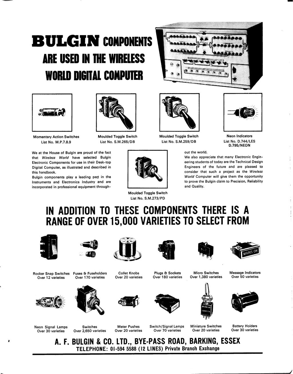
37
38
39
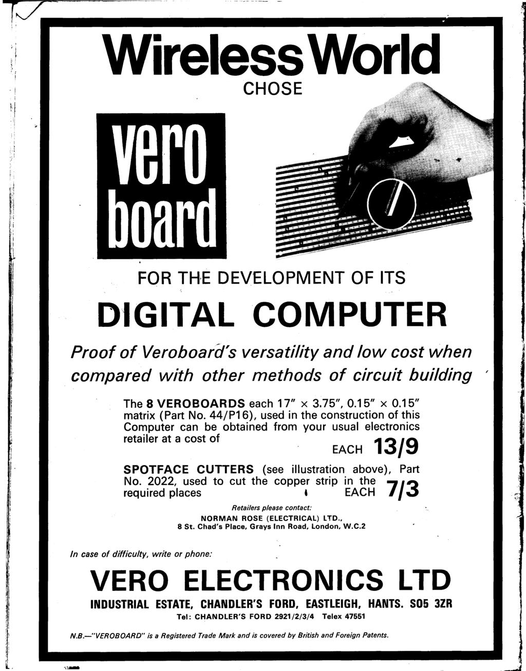
40
MODULE 3. Combinational & Sequential logic
 MODULE 3 Combinational & Sequential logic Combinational Logic Introduction Logic circuit may be classified into two categories. Combinational logic circuits 2. Sequential logic circuits A combinational
Analogue Versus Digital [5 M]
![Analogue Versus Digital [5 M]](/thumbs/93/111640168.jpg "Analogue Versus Digital [5 M]") Q.1 a. Analogue Versus Digital [5 M] There are two basic ways of representing the numerical values of the various physical quantities with which we constantly deal in our day-to-day lives. One of the ways,
Q.1 a. Analogue Versus Digital [5 M] There are two basic ways of representing the numerical values of the various physical quantities with which we constantly deal in our day-to-day lives. One of the ways,
The basic logic gates are the inverter (or NOT gate), the AND gate, the OR gate and the exclusive-or gate (XOR). If you put an inverter in front of
, the AND gate, the OR gate and the exclusive-or gate (XOR). If you put an inverter in front of") 1 The basic logic gates are the inverter (or NOT gate), the AND gate, the OR gate and the exclusive-or gate (XOR). If you put an inverter in front of the AND gate, you get the NAND gate etc. 2 One of the
1 The basic logic gates are the inverter (or NOT gate), the AND gate, the OR gate and the exclusive-or gate (XOR). If you put an inverter in front of the AND gate, you get the NAND gate etc. 2 One of the
Solution to Digital Logic )What is the magnitude comparator? Design a logic circuit for 4 bit magnitude comparator and explain it,
What is the magnitude comparator? Design a logic circuit for 4 bit magnitude comparator and explain it,") Solution to Digital Logic -2067 Solution to digital logic 2067 1.)What is the magnitude comparator? Design a logic circuit for 4 bit magnitude comparator and explain it, A Magnitude comparator is a combinational
Solution to Digital Logic -2067 Solution to digital logic 2067 1.)What is the magnitude comparator? Design a logic circuit for 4 bit magnitude comparator and explain it, A Magnitude comparator is a combinational
AC103/AT103 ANALOG & DIGITAL ELECTRONICS JUN 2015
 Q.2 a. Draw and explain the V-I characteristics (forward and reverse biasing) of a pn junction. (8) Please refer Page No 14-17 I.J.Nagrath Electronic Devices and Circuits 5th Edition. b. Draw and explain
UNIT III. Combinational Circuit- Block Diagram. Sequential Circuit- Block Diagram
 UNIT III INTRODUCTION In combinational logic circuits, the outputs at any instant of time depend only on the input signals present at that time. For a change in input, the output occurs immediately. Combinational
Introduction to Digital Electronics
 Introduction to Digital Electronics by Agner Fog, 2018-10-15. Contents 1. Number systems... 3 1.1. Decimal, binary, and hexadecimal numbers... 3 1.2. Conversion from another number system to decimal...
1. Convert the decimal number to binary, octal, and hexadecimal.
 1. Convert the decimal number 435.64 to binary, octal, and hexadecimal. 2. Part A. Convert the circuit below into NAND gates. Insert or remove inverters as necessary. Part B. What is the propagation delay
Chapter 3: Sequential Logic Systems
 Chapter 3: Sequential Logic Systems 1. The S-R Latch Learning Objectives: At the end of this topic you should be able to: design a Set-Reset latch based on NAND gates; complete a sequential truth table
UNIT IV. Sequential circuit
 UNIT IV Sequential circuit Introduction In the previous session, we said that the output of a combinational circuit depends solely upon the input. The implication is that combinational circuits have no
QUICK GUIDE COMPUTER LOGICAL ORGANIZATION - OVERVIEW
 QUICK GUIDE http://www.tutorialspoint.com/computer_logical_organization/computer_logical_organization_quick_guide.htm COMPUTER LOGICAL ORGANIZATION - OVERVIEW Copyright tutorialspoint.com In the modern
Chapter 3. Boolean Algebra and Digital Logic
 Chapter 3 Boolean Algebra and Digital Logic Chapter 3 Objectives Understand the relationship between Boolean logic and digital computer circuits. Learn how to design simple logic circuits. Understand how
Chapter 5 Flip-Flops and Related Devices
 Chapter 5 Flip-Flops and Related Devices Chapter 5 Objectives Selected areas covered in this chapter: Constructing/analyzing operation of latch flip-flops made from NAND or NOR gates. Differences of synchronous/asynchronous
Find the equivalent decimal value for the given value Other number system to decimal ( Sample)
") VELAMMAL COLLEGE OF ENGINEERING AND TECHNOLOGY, MADURAI 65 009 Department of Information Technology Model Exam-II-Question bank PART A (Answer for all Questions) (8 X = 6) K CO Marks Find the equivalent
VELAMMAL COLLEGE OF ENGINEERING AND TECHNOLOGY, MADURAI 65 009 Department of Information Technology Model Exam-II-Question bank PART A (Answer for all Questions) (8 X = 6) K CO Marks Find the equivalent
UNIT 1: DIGITAL LOGICAL CIRCUITS What is Digital Computer? OR Explain the block diagram of digital computers.
 UNIT 1: DIGITAL LOGICAL CIRCUITS What is Digital Computer? OR Explain the block diagram of digital computers. Digital computer is a digital system that performs various computational tasks. The word DIGITAL
FLIP-FLOPS AND RELATED DEVICES
 C H A P T E R 5 FLIP-FLOPS AND RELATED DEVICES OUTLINE 5- NAND Gate Latch 5-2 NOR Gate Latch 5-3 Troubleshooting Case Study 5-4 Digital Pulses 5-5 Clock Signals and Clocked Flip-Flops 5-6 Clocked S-R Flip-Flop
WINTER 15 EXAMINATION Model Answer
 Important Instructions to examiners: 1) The answers should be examined by key words and not as word-to-word as given in the model answer scheme. 2) The model answer and the answer written by candidate
Chapter 4. Logic Design
 Chapter 4 Logic Design 4.1 Introduction. In previous Chapter we studied gates and combinational circuits, which made by gates (AND, OR, NOT etc.). That can be represented by circuit diagram, truth table
DEPARTMENT OF COMPUTER SCIENCE & ENGINEERING
 DRONACHARYA GROUP OF INSTITUTIONS, GREATER NOIDA Affiliated to Mahamaya Technical University, Noida Approved by AICTE DEPARTMENT OF COMPUTER SCIENCE & ENGINEERING Lab Manual for Computer Organization Lab
The word digital implies information in computers is represented by variables that take a limited number of discrete values.
 Class Overview Cover hardware operation of digital computers. First, consider the various digital components used in the organization and design. Second, go through the necessary steps to design a basic
Sequential Logic Basics
 Sequential Logic Basics Unlike Combinational Logic circuits that change state depending upon the actual signals being applied to their inputs at that time, Sequential Logic circuits have some form of inherent
DIGITAL SYSTEM FUNDAMENTALS (ECE421) DIGITAL ELECTRONICS FUNDAMENTAL (ECE422) COUNTERS
 DIGITAL ELECTRONICS FUNDAMENTAL (ECE422) COUNTERS") COURSE / CODE DIGITAL SYSTEM FUNDAMENTALS (ECE421) DIGITAL ELECTRONICS FUNDAMENTAL (ECE422) COUNTERS One common requirement in digital circuits is counting, both forward and backward. Digital clocks and
COURSE / CODE DIGITAL SYSTEM FUNDAMENTALS (ECE421) DIGITAL ELECTRONICS FUNDAMENTAL (ECE422) COUNTERS One common requirement in digital circuits is counting, both forward and backward. Digital clocks and
Logic Design II (17.342) Spring Lecture Outline
 Spring Lecture Outline") Logic Design II (17.342) Spring 2012 Lecture Outline Class # 05 February 23, 2012 Dohn Bowden 1 Today s Lecture Analysis of Clocked Sequential Circuits Chapter 13 2 Course Admin 3 Administrative Admin
Logic Design II (17.342) Spring 2012 Lecture Outline Class # 05 February 23, 2012 Dohn Bowden 1 Today s Lecture Analysis of Clocked Sequential Circuits Chapter 13 2 Course Admin 3 Administrative Admin
Flip Flop. S-R Flip Flop. Sequential Circuits. Block diagram. Prepared by:- Anwar Bari
 Sequential Circuits The combinational circuit does not use any memory. Hence the previous state of input does not have any effect on the present state of the circuit. But sequential circuit has memory
Contents Circuits... 1
 Contents Circuits... 1 Categories of Circuits... 1 Description of the operations of circuits... 2 Classification of Combinational Logic... 2 1. Adder... 3 2. Decoder:... 3 Memory Address Decoder... 5 Encoder...
MC9211 Computer Organization
 MC9211 Computer Organization Unit 2 : Combinational and Sequential Circuits Lesson2 : Sequential Circuits (KSB) (MCA) (2009-12/ODD) (2009-10/1 A&B) Coverage Lesson2 Outlines the formal procedures for the
Department of CSIT. Class: B.SC Semester: II Year: 2013 Paper Title: Introduction to logics of Computer Max Marks: 30
 Department of CSIT Class: B.SC Semester: II Year: 2013 Paper Title: Introduction to logics of Computer Max Marks: 30 Section A: (All 10 questions compulsory) 10X1=10 Very Short Answer Questions: Write
Notes on Digital Circuits
 PHYS 331: Junior Physics Laboratory I Notes on Digital Circuits Digital circuits are collections of devices that perform logical operations on two logical states, represented by voltage levels. Standard
MAHARASHTRA STATE BOARD OF TECHNICAL EDUCATION (Autonomous) (ISO/IEC Certified)
 (ISO/IEC Certified)") Important Instructions to examiners: 1) The answers should be examined by key words and not as word-to-word as given in the model answer scheme. 2) The model answer and the answer written by candidate
Important Instructions to examiners: 1) The answers should be examined by key words and not as word-to-word as given in the model answer scheme. 2) The model answer and the answer written by candidate
NORTHWESTERN UNIVERSITY TECHNOLOGICAL INSTITUTE
 NORTHWESTERN UNIVERSITY TECHNOLOGICL INSTITUTE ECE 270 Experiment #8 DIGITL CIRCUITS Prelab 1. Draw the truth table for the S-R Flip-Flop as shown in the textbook. Draw the truth table for Figure 7. 2.
BCN1043. By Dr. Mritha Ramalingam. Faculty of Computer Systems & Software Engineering
 BCN1043 By Dr. Mritha Ramalingam Faculty of Computer Systems & Software Engineering mritha@ump.edu.my http://ocw.ump.edu.my/ authors Dr. Mohd Nizam Mohmad Kahar (mnizam@ump.edu.my) Jamaludin Sallim (jamal@ump.edu.my)
Vignana Bharathi Institute of Technology UNIT 4 DLD
 DLD UNIT IV Synchronous Sequential Circuits, Latches, Flip-flops, analysis of clocked sequential circuits, Registers, Shift registers, Ripple counters, Synchronous counters, other counters. Asynchronous
CS302 Digital Logic Design Solved Objective Midterm Papers For Preparation of Midterm Exam
 CS302 Digital Logic Design Solved Objective Midterm Papers For Preparation of Midterm Exam MIDTERM EXAMINATION Spring 2012 Question No: 1 ( Marks: 1 ) - Please choose one A SOP expression is equal to 1
DIGITAL SYSTEM FUNDAMENTALS (ECE421) DIGITAL ELECTRONICS FUNDAMENTAL (ECE422) LATCHES and FLIP-FLOPS
 DIGITAL ELECTRONICS FUNDAMENTAL (ECE422) LATCHES and FLIP-FLOPS") COURSE / CODE DIGITAL SYSTEM FUNDAMENTALS (ECE421) DIGITAL ELECTRONICS FUNDAMENTAL (ECE422) LATCHES and FLIP-FLOPS In the same way that logic gates are the building blocks of combinatorial circuits, latches
COURSE / CODE DIGITAL SYSTEM FUNDAMENTALS (ECE421) DIGITAL ELECTRONICS FUNDAMENTAL (ECE422) LATCHES and FLIP-FLOPS In the same way that logic gates are the building blocks of combinatorial circuits, latches
Laboratory 10. Required Components: Objectives. Introduction. Digital Circuits - Logic and Latching (modified from lab text by Alciatore)
") Laboratory 10 Digital Circuits - Logic and Latching (modified from lab text by Alciatore) Required Components: 1x 330 resistor 4x 1k resistor 2x 0.F capacitor 1x 2N3904 small signal transistor 1x LED 1x
Laboratory 10 Digital Circuits - Logic and Latching (modified from lab text by Alciatore) Required Components: 1x 330 resistor 4x 1k resistor 2x 0.F capacitor 1x 2N3904 small signal transistor 1x LED 1x
Computer Architecture and Organization
 A-1 Appendix A - Digital Logic Computer Architecture and Organization Miles Murdocca and Vincent Heuring Appendix A Digital Logic A-2 Appendix A - Digital Logic Chapter Contents A.1 Introduction A.2 Combinational
An Introduction to Digital Logic
 An Introduction to Digital Logic Other titles in Electrical and Electronic Engineering B. A. Gregory: An Introduction to Electrical Instrumentation P. and A. Lynn: An Introduction to the Analysis and Processing
EE292: Fundamentals of ECE
 EE292: Fundamentals of ECE Fall 2012 TTh 10:00-11:15 SEB 1242 Lecture 23 121120 http://www.ee.unlv.edu/~b1morris/ee292/ 2 Outline Review Combinatorial Logic Sequential Logic 3 Combinatorial Logic Circuits
EXPERIMENT #6 DIGITAL BASICS
 EXPERIMENT #6 DIGITL SICS Digital electronics is based on the binary number system. Instead of having signals which can vary continuously as in analog circuits, digital signals are characterized by only
MUHAMMAD NAEEM LATIF MCS 3 RD SEMESTER KHANEWAL
 1. A stage in a shift register consists of (a) a latch (b) a flip-flop (c) a byte of storage (d) from bits of storage 2. To serially shift a byte of data into a shift register, there must be (a) one click
Notes on Digital Circuits
 PHYS 331: Junior Physics Laboratory I Notes on Digital Circuits Digital circuits are collections of devices that perform logical operations on two logical states, represented by voltage levels. Standard
Unit 11. Latches and Flip-Flops
 Unit 11 Latches and Flip-Flops 1 Combinational Circuits A combinational circuit consists of logic gates whose outputs, at any time, are determined by combining the values of the inputs. For n input variables,
SEMESTER ONE EXAMINATIONS 2002
 SEMESTER ONE EXAMINATIONS 2002 EE101 Digital Electronics Solutions Question 1. An assembly line has 3 failsafe sensors and 1 emergency shutdown switch. The Line should keep moving unless any of the following
General description. The Pilot ACE is a serial machine using mercury delay line storage
 Chapter 11 The Pilot ACE 1 /. H. Wilkinson Introduction A machine which was almost identical with the Pilot ACE was first designed by the staff of the Mathematics Division at the suggestion of Dr. H. D.
1. a) For the circuit shown in figure 1.1, draw a truth table showing the output Q for all combinations of inputs A, B and C. [4] Figure 1.
![1. a) For the circuit shown in figure 1.1, draw a truth table showing the output Q for all combinations of inputs A, B and C. [4] Figure 1.](/thumbs/88/117492374.jpg "1. a) For the circuit shown in figure 1.1, draw a truth table showing the output Q for all combinations of inputs A, B and C. [4] Figure 1.") [Question 1 is compulsory] 1. a) For the circuit shown in figure 1.1, draw a truth table showing the output Q for all combinations of inputs A, B and C. Figure 1.1 b) Minimize the following Boolean functions:
[Question 1 is compulsory] 1. a) For the circuit shown in figure 1.1, draw a truth table showing the output Q for all combinations of inputs A, B and C. Figure 1.1 b) Minimize the following Boolean functions:
Digital Circuits. Electrical & Computer Engineering Department (ECED) Course Notes ECED2200. ECED2200 Digital Circuits Notes 2012 Dalhousie University
 Course Notes ECED2200. ECED2200 Digital Circuits Notes 2012 Dalhousie University") 1 Digital Circuits Electrical & Computer Engineering Department (ECED) Course Notes ECED2200 2 Table of Contents Digital Circuits... 7 Logic Gates... 8 AND Gate... 8 OR Gate... 9 NOT Gate... 10 NOR Gate...
1 Digital Circuits Electrical & Computer Engineering Department (ECED) Course Notes ECED2200 2 Table of Contents Digital Circuits... 7 Logic Gates... 8 AND Gate... 8 OR Gate... 9 NOT Gate... 10 NOR Gate...
Computer Systems Architecture
 Computer Systems Architecture Fundamentals Of Digital Logic 1 Our Goal Understand Fundamentals and basics Concepts How computers work at the lowest level Avoid whenever possible Complexity Implementation
UNIT-3: SEQUENTIAL LOGIC CIRCUITS
 UNIT-3: SEQUENTIAL LOGIC CIRCUITS STRUCTURE 3. Objectives 3. Introduction 3.2 Sequential Logic Circuits 3.2. NAND Latch 3.2.2 RS Flip-Flop 3.2.3 D Flip-Flop 3.2.4 JK Flip-Flop 3.2.5 Edge Triggered RS Flip-Flop
Module -5 Sequential Logic Design
 Module -5 Sequential Logic Design 5.1. Motivation: In digital circuit theory, sequential logic is a type of logic circuit whose output depends not only on the present value of its input signals but on
Sequential Logic Circuits
 Sequential Logic Circuits By Dr. M. Hebaishy Digital Logic Design Ch- Rem.!) Types of Logic Circuits Combinational Logic Memoryless Outputs determined by current values of inputs Sequential Logic Has memory
The reduction in the number of flip-flops in a sequential circuit is referred to as the state-reduction problem.
 State Reduction The reduction in the number of flip-flops in a sequential circuit is referred to as the state-reduction problem. State-reduction algorithms are concerned with procedures for reducing the
EEE130 Digital Electronics I Lecture #1_2. Dr. Shahrel A. Suandi
 EEE130 Digital Electronics I Lecture #1_2 Dr. Shahrel A. Suandi 1-4 Overview of Basic Logic Functions Digital systems are generally built from combinations of NOT, AND and OR logic elements The combinations
Engineering College. Electrical Engineering Department. Digital Electronics Lab
 Engineering College Electrical Engineering Department Digital Electronics Lab Prepared by: Dr. Samer Mayaleh Eng. Nuha Odeh 2009/2010-1 - CONTENTS Experiment Name Page 1- Measurement of Basic Logic Gates
CHAPTER 4: Logic Circuits
 CHAPTER 4: Logic Circuits II. Sequential Circuits Combinational circuits o The outputs depend only on the current input values o It uses only logic gates, decoders, multiplexers, ALUs Sequential circuits
Chapter 5: Synchronous Sequential Logic
 Chapter 5: Synchronous Sequential Logic NCNU_2016_DD_5_1 Digital systems may contain memory for storing information. Combinational circuits contains no memory elements the outputs depends only on the inputs
Decade Counters Mod-5 counter: Decade Counter:
 Decade Counters We can design a decade counter using cascade of mod-5 and mod-2 counters. Mod-2 counter is just a single flip-flop with the two stable states as 0 and 1. Mod-5 counter: A typical mod-5
Registers and Counters
 Registers and Counters Clocked sequential circuit = F/Fs and combinational gates Register Group of flip-flops (share a common clock and capable of storing one bit of information) Consist of a group of
(Refer Slide Time: 2:03)
") (Refer Slide Time: 2:03) Digital Circuits and Systems Prof. S. Srinivasan Department of Electrical Engineering Indian Institute of Technology, Madras Lecture # 22 Application of Shift Registers Today we
(Refer Slide Time: 2:03) Digital Circuits and Systems Prof. S. Srinivasan Department of Electrical Engineering Indian Institute of Technology, Madras Lecture # 22 Application of Shift Registers Today we
D Latch (Transparent Latch)
") D Latch (Transparent Latch) -One way to eliminate the undesirable condition of the indeterminate state in the SR latch is to ensure that inputs S and R are never equal to 1 at the same time. This is done
D Latch (Transparent Latch) -One way to eliminate the undesirable condition of the indeterminate state in the SR latch is to ensure that inputs S and R are never equal to 1 at the same time. This is done
Reaction Game Kit MitchElectronics 2019
 Reaction Game Kit MitchElectronics 2019 www.mitchelectronics.co.uk CONTENTS Schematic 3 How It Works 4 Materials 6 Construction 8 Important Information 9 Page 2 SCHEMATIC Page 3 SCHEMATIC EXPLANATION The
SEQUENTIAL LOGIC. Satish Chandra Assistant Professor Department of Physics P P N College, Kanpur
 SEQUENTIAL LOGIC Satish Chandra Assistant Professor Department of Physics P P N College, Kanpur www.satish0402.weebly.com OSCILLATORS Oscillators is an amplifier which derives its input from output. Oscillators
Previous Lecture Sequential Circuits. Slide Summary of contents covered in this lecture. (Refer Slide Time: 01:55)
") Previous Lecture Sequential Circuits Digital VLSI System Design Prof. S. Srinivasan Department of Electrical Engineering Indian Institute of Technology, Madras Lecture No 7 Sequential Circuit Design Slide
Previous Lecture Sequential Circuits Digital VLSI System Design Prof. S. Srinivasan Department of Electrical Engineering Indian Institute of Technology, Madras Lecture No 7 Sequential Circuit Design Slide
Synchronous Sequential Logic
 Synchronous Sequential Logic Ranga Rodrigo August 2, 2009 1 Behavioral Modeling Behavioral modeling represents digital circuits at a functional and algorithmic level. It is used mostly to describe sequential
EECS 140 Laboratory Exercise 7 PLD Programming
 1. Objectives EECS 140 Laboratory Exercise 7 PLD Programming A. Become familiar with the capabilities of Programmable Logic Devices (PLDs) B. Implement a simple combinational logic circuit using a PLD.
Introduction to Digital Logic Missouri S&T University CPE 2210 Exam 3 Logistics
 Introduction to Digital Logic Missouri S&T University CPE 2210 Exam 3 Logistics Egemen K. Çetinkaya Egemen K. Çetinkaya Department of Electrical & Computer Engineering Missouri University of Science and
Name Of The Experiment: Sequential circuit design Latch, Flip-flop and Registers
 EEE 304 Experiment No. 07 Name Of The Experiment: Sequential circuit design Latch, Flip-flop and Registers Important: Submit your Prelab at the beginning of the lab. Prelab 1: Construct a S-R Latch and
CS 61C: Great Ideas in Computer Architecture
 CS 6C: Great Ideas in Computer Architecture Combinational and Sequential Logic, Boolean Algebra Instructor: Alan Christopher 7/23/24 Summer 24 -- Lecture #8 Review of Last Lecture OpenMP as simple parallel
Semester 6 DIGITAL ELECTRONICS- core subject -10 Credit-4
 Semester 6 DIGITAL ELECTRONICS- core subject -10 Credit-4 Unit I Number system, Binary, decimal, octal, hexadecimal-conversion from one another-binary addition, subtraction, multiplication, division-binary
Digital Principles and Design
 Digital Principles and Design Donald D. Givone University at Buffalo The State University of New York Grauu Boston Burr Ridge, IL Dubuque, IA Madison, Wl New York San Francisco St. Louis Bangkok Bogota
DIGITAL ELECTRONICS: LOGIC AND CLOCKS
 DIGITL ELECTRONICS: LOGIC ND CLOCKS L 6 INTRO: INTRODUCTION TO DISCRETE DIGITL LOGIC, MEMORY, ND CLOCKS GOLS In this experiment, we will learn about the most basic elements of digital electronics, from
CHAPTER 4 RESULTS & DISCUSSION
 CHAPTER 4 RESULTS & DISCUSSION 3.2 Introduction This project aims to prove that Modified Baugh-Wooley Two s Complement Signed Multiplier is one of the high speed multipliers. The schematic of the multiplier
Logic Design Viva Question Bank Compiled By Channveer Patil
 Logic Design Viva Question Bank Compiled By Channveer Patil Title of the Practical: Verify the truth table of logic gates AND, OR, NOT, NAND and NOR gates/ Design Basic Gates Using NAND/NOR gates. Q.1
Logic Design II (17.342) Spring Lecture Outline
 Spring Lecture Outline") Logic Design II (17.342) Spring 2012 Lecture Outline Class # 03 February 09, 2012 Dohn Bowden 1 Today s Lecture Registers and Counters Chapter 12 2 Course Admin 3 Administrative Admin for tonight Syllabus
Logic Design II (17.342) Spring 2012 Lecture Outline Class # 03 February 09, 2012 Dohn Bowden 1 Today s Lecture Registers and Counters Chapter 12 2 Course Admin 3 Administrative Admin for tonight Syllabus
St. MARTIN S ENGINEERING COLLEGE
 St. MARTIN S ENGINEERING COLLEGE Dhulapally, Kompally, Secunderabad-500014. Branch Year&Sem Subject Name : Electronics and Communication Engineering : II B. Tech I Semester : SWITCHING THEORY AND LOGIC
Introduction. Serial In - Serial Out Shift Registers (SISO)
") Introduction Shift registers are a type of sequential logic circuit, mainly for storage of digital data. They are a group of flip-flops connected in a chain so that the output from one flip-flop becomes
Introduction Shift registers are a type of sequential logic circuit, mainly for storage of digital data. They are a group of flip-flops connected in a chain so that the output from one flip-flop becomes
BISHOP ANSTEY HIGH SCHOOL & TRINITY COLLEGE EAST SIXTH FORM CXC CAPE PHYSICS, UNIT 2 Ms. S. S. CALBIO NOTES lesson #39
 BISHOP ANSTEY HIGH SCHOOL & TRINITY COLLEGE EAST SIXTH FORM CXC CAPE PHYSICS, UNIT 2 Ms. S. S. CALBIO NOTES lesson #39 Objectives: Students should be able to Thursday 21 st January 2016 @ 10:45 am Module
WINTER 14 EXAMINATION
 Subject Code: 17320 WINTER 14 EXAMINATION Model Answer Important Instructions to examiners: 1) The answers should be examined by key words and not as word-to-word as given in the model answer scheme. 2)
Registers and Counters
 Registers and Counters Clocked sequential circuit = F/Fs and combinational gates Register Group of flip-flops (share a common clock and capable of storing one bit of information) Consist of a group of
Music Electronics Finally DeMorgan's Theorem establishes two very important simplifications 3 : Multiplexers
 Music Electronics Finally DeMorgan's Theorem establishes two very important simplifications 3 : ( A B )' = A' + B' ( A + B )' = A' B' Multiplexers A digital multiplexer is a switching element, like a mechanical
CHAPTER 4: Logic Circuits
 CHAPTER 4: Logic Circuits II. Sequential Circuits Combinational circuits o The outputs depend only on the current input values o It uses only logic gates, decoders, multiplexers, ALUs Sequential circuits
EE 367 Lab Part 1: Sequential Logic
 EE367: Introduction to Microprocessors Section 1.0 EE 367 Lab Part 1: Sequential Logic Contents 1 Preface 1 1.1 Things you need to do before arriving in the Laboratory............... 2 1.2 Summary of material
North Shore Community College
 North Shore Community College Course Number: IEL217 Section: MAL Course Name: Digital Electronics 1 Semester: Credit: 4 Hours: Three hours of Lecture, Two hours Laboratory per week Thursdays 8:00am (See
Logic and Computer Design Fundamentals. Chapter 7. Registers and Counters
 Logic and Computer Design Fundamentals Chapter 7 Registers and Counters Registers Register a collection of binary storage elements In theory, a register is sequential logic which can be defined by a state
The outputs are formed by a combinational logic function of the inputs to the circuit or the values stored in the flip-flops (or both).
.") 1 The outputs are formed by a combinational logic function of the inputs to the circuit or the values stored in the flip-flops (or both). The value that is stored in a flip-flop when the clock pulse occurs
1 The outputs are formed by a combinational logic function of the inputs to the circuit or the values stored in the flip-flops (or both). The value that is stored in a flip-flop when the clock pulse occurs
Chapter 4: One-Shots, Counters, and Clocks
 Chapter 4: One-Shots, Counters, and Clocks I. The Monostable Multivibrator (One-Shot) The timing pulse is one of the most common elements of laboratory electronics. Pulses can control logical sequences
Digital Circuits I and II Nov. 17, 1999
 Physics 623 Digital Circuits I and II Nov. 17, 1999 Digital Circuits I 1 Purpose To introduce the basic principles of digital circuitry. To understand the small signal response of various gates and circuits
Chapter 6. Flip-Flops and Simple Flip-Flop Applications
 Chapter 6 Flip-Flops and Simple Flip-Flop Applications Basic bistable element It is a circuit having two stable conditions (states). It can be used to store binary symbols. J. C. Huang, 2004 Digital Logic
MAHARASHTRA STATE BOARD OF TECHNICAL EDUCATION (Autonomous) (ISO/IEC Certified) WINTER 2018 EXAMINATION MODEL ANSWER
 (ISO/IEC Certified) WINTER 2018 EXAMINATION MODEL ANSWER") Important Instructions to examiners: 1) The answers should be examined by key words and not as word-to-word as given in themodel answer scheme. 2) The model answer and the answer written by candidate may
Important Instructions to examiners: 1) The answers should be examined by key words and not as word-to-word as given in themodel answer scheme. 2) The model answer and the answer written by candidate may
R13 SET - 1 '' ''' '' ' '''' Code No: RT21053
 SET - 1 1. a) What are the characteristics of 2 s complement numbers? b) State the purpose of reducing the switching functions to minimal form. c) Define half adder. d) What are the basic operations in
Digital Systems Laboratory 3 Counters & Registers Time 4 hours
 Digital Systems Laboratory 3 Counters & Registers Time 4 hours Aim: To investigate the counters and registers constructed from flip-flops. Introduction: In the previous module, you have learnt D, S-R,
Review of digital electronics. Storage units Sequential circuits Counters Shifters
 Review of digital electronics Storage units Sequential circuits ounters Shifters ounting in Binary A counter can form the same pattern of 0 s and 1 s with logic levels. The first stage in the counter represents
Principles of Computer Architecture. Appendix A: Digital Logic
 A-1 Appendix A - Digital Logic Principles of Computer Architecture Miles Murdocca and Vincent Heuring Appendix A: Digital Logic A-2 Appendix A - Digital Logic Chapter Contents A.1 Introduction A.2 Combinational
COMP12111: Fundamentals of Computer Engineering
 COMP2: Fundamentals of Computer Engineering Part I Course Overview & Introduction to Logic Paul Nutter Introduction What is this course about? Computer hardware design o not electronics nothing nasty like
DIGITAL LOGIC HANDBOOK
 DIGITAL LOGIC HANDBOOK COPYRIGHT, 1961, BY DIGITAL EQUIPMENT CORPORATION First Edition - September, 1960 Second Edition - November, 1960 Third Edition - March, 1961 PRINTED IN THE UNITED STATES OF AMERICA
Long and Fast Up/Down Counters Pushpinder Kaur CHOUHAN 6 th Jan, 2003
 1 Introduction Long and Fast Up/Down Counters Pushpinder Kaur CHOUHAN 6 th Jan, 2003 Circuits for counting both forward and backward events are frequently used in computers and other digital systems. Digital
B. Sc. III Semester (Electronics) - ( ) Digital Electronics-II) BE-301 MODEL ANSWER (AS-2791)
 - ( ) Digital Electronics-II) BE-301 MODEL ANSWER (AS-2791)") B. Sc. III Semester (Electronics) - (2013-14) Digital Electronics-II) BE-301 MODEL ANSWER (AS-2791) Section-[A] i. (B) ii. (A) iii. (D) iv. (C) v. (C) vi. (C) vii. (D) viii. (B) Ans-(ix): In JK flip flop
B. Sc. III Semester (Electronics) - (2013-14) Digital Electronics-II) BE-301 MODEL ANSWER (AS-2791) Section-[A] i. (B) ii. (A) iii. (D) iv. (C) v. (C) vi. (C) vii. (D) viii. (B) Ans-(ix): In JK flip flop
NH 67, Karur Trichy Highways, Puliyur C.F, Karur District UNIT-III SEQUENTIAL CIRCUITS
 NH 67, Karur Trichy Highways, Puliyur C.F, 639 114 Karur District DEPARTMENT OF ELETRONICS AND COMMUNICATION ENGINEERING COURSE NOTES SUBJECT: DIGITAL ELECTRONICS CLASS: II YEAR ECE SUBJECT CODE: EC2203
Physics 323. Experiment # 10 - Digital Circuits
 Physics 323 Experiment # 10 - Digital Circuits Purpose This is a brief introduction to digital (logic) circuits using both combinational and sequential logic. The basic building blocks will be the Transistor
DEC BUILDING BLOCK LOGIC
 ., DEC BUILDING BLOCK LOGIC PER COPY $1.00 DEC BUILDING BLOCK LOGIC digital equipment corporation MAYNARD, MASSACHUSETTS COPYRIGHT, 1960, BY DIGITAL EQUIPMENT CORPORATION PRINTED IN THE UNITED STATES
ME 515 Mechatronics. Introduction to Digital Electronics
 ME 55 Mechatronics /5/26 ME 55 Mechatronics Digital Electronics Asanga Ratnaweera Department of Faculty of Engineering University of Peradeniya Tel: 8239 (3627) Email: asangar@pdn.ac.lk Introduction to