7454 4x2 AND/NOR x4 AND/NOR x2 Ex-NOR/Ex-OR x NAND 2x INVERTER X8 OR/NOR 14. EXPANDER x4 AND EXPANDER 14
|
|
|
- Oliver Bridges
- 6 years ago
- Views:
Transcription
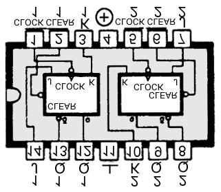
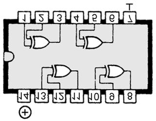
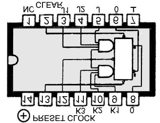
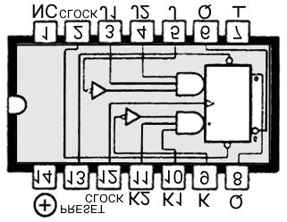
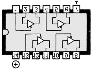
1 NAND GATES x2-Input x2-Input x2-Input x3-Input x3-Input x4-Input x4-Input x2-Input 15V x8-Input x13-Input x12-Input 16 NAND-BUFFER/DRIVER GATES x2-Input Buffer x2-Input Buffer x2-Input Buffer x4-Input Buffer 14 NOR GATES x2 NOR x4 NOR x4 NOR x3 NOR x5 NOR x4 NOR 14 NOR-BUFFER/DRIVER GATES x2 NOR Buffer x2 NOR Buffer 14 AND GATES x2 AND x2 AND x3 AND x3 AND x4 AND 14 OR GATES x2 OR x3 OR 14 EXCLUSIVE NOR GATES x2 Ex-NOR 14 EXCLUSIVE OR GATES x2 Ex OR x2 Ex OR x2 Ex OR 14 COMBINED GATES 7450 Dual 2x2 AND/NOR Dual 2x3 AND/NOR x2 AND/NOR x2 AND/NOR x4 AND/NOR x2 Ex-NOR/Ex-OR x NAND 2x INVERTER X8 OR/NOR 14 SCHMITT-TRIGGER x4 NAND - Shmitt Trigger x Schmitt - Trigger/Inverter x4 NAND Schmitt Trigger x Schmitt Trigger/Inverter x2 NAND Schmitt Trigger x2 NAND Schmitt-Trigger x Schmitt Trigger/Inverter 14 EXPANDER x4 AND EXPANDER 14 BUFFER/DRIVER INVERTING x Inverter x Inverter x Inverter 30V x Inverter 15V 14 NON-INVERTING x Driver x Driver x Driver x Buffer (Open Drain) x Buffer 16 EDGE TRIGGERED J-K FLIP-FLOP x Flip-Flop with Preset and Clear x Flip-Flop with Preset and Clear x Flip-Flop with Preset and Clear x Flip-Flop with Preset x Flip-Flop with Preset and Clear 14 IMPULS TRIGGERED J-K FLIP-FLOP x Flip-Flop with Preset and Clear x Flip-Flop with Preset and Clear x Flip-Flop with Preset and Clear x Flip-Flop x Flip-Flop 16 EDGE/IMPULS TRIGGERED J-K FLIP-FLOP x Flip-Flop with Clear x Flip-Flop with Preset and Clear x Flip-Flop with Preset and Clear x Flip-Flop with Clear 14 RS-FLIPFLOPS x NAND Flip-Flop
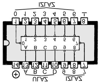
2 NON INVERTING D-LATCHES x2-bit Latch x4-bit Latch with Clear bit Latch with Enable bit Latch with Enable bit Latch with Enable 20 INVERTING D-LATCHES bit Latch with Enable bit Latch with Enable 20 NON INVERTING/INVERTING D-LATCHES x2-bit Latch x2-bit Latch 16 ADDRESSABLE D-LATCHES x4-bit Adressable Latch bit Adressable Latch 16 NON INVERTING D-FLIPFLOP bit D-Register bit D-Register bit D-Register bit Register with Enable bit D-Register bit D-Register bit Register with Enable 20 INVERTING D-FLIPFLOP bit Register with enable bit Register with enable bit Register with enable 20 NON INVERTING/INVERTING D-FLIPFLOP x Flip-Flop with Preset and Clear x Flip-Flop with Clear x Flip-Flop with Clear 16 MONOFLOPS D-FLIPFLOP x Monoflop non Retriggerable x Monoflop Retriggerable x Monoflop Retriggerable x4-bit Pipeline Register x Monoflop non Retriggerable x Monoflop Retriggerable 16 BINARY UP COUNTER bit Asynchronous bit Asynchronous bit Synhr. with Preset and Clear bit Synhr. with Preset and Clear bit Asynchronous with Preset bit Asynchronous with Preset bit Asynchronous x4-bit Asynchronous bit Asynchronous with Register bit Asynchronous with Preset bit Asynchronous bit Asynchronous bit Asynchronous bit Asynchronous x4-bit Synchronous 16 BINARY UP/DOWN COUNTER bit Synchronous with Preset bit Synchronous with Preset bit Synchronous with Preset bit Synchronous with Preset 16 BINARY DOWN COUNTER bit Synchronous 16 DECIMAL UP COUNTER bit Asynchronous bit Synch. with Decimal-Decod./Drv bit Synch. with 7-Segment Decoder bit Synch. with 7-Segment Decoder bit Synhr. with Preset and Clear bit Synhr. with Preset and Clear bit Synhr. with Preset bit Asynhronous with Preset bit Asynhronous x4-bit Asynhronous x4-bit Asynhronous 16 DECIMAL UP/DOWN COUNTER bit Synchronous with Preset bit Synchronous with Preset bit Synchronous with Preset 16 MISCELLANECUS COUNTER Display Counter Johnson Decade Counter 16 SERIAL SHIFT REGISTER bit Singel Right 14 SERIAL INPUT/PARALLEL OUTPUT SHIFT REGISTER bit Right bit Right 16 PARALLEL INPUT SHIFT REGISTER bit NOR Input bit with Clear bit with Clear bit
3 PARALLEL OUTPUT SHIFT REGISTER bit bit with Latch 16 PARALLEL OUTPUT/INPUT SHIFT REGISTER bit Right/Left bit Right bit Right with Clear bit Right with Clear bit Right/Left bit Right/Left with Clear bit Right/Left bit Right with Clear bit Right with Clear bit Right/Left bit Right bit Right/Left bit Right with Clear bit Right with Input Latch 16 OSCILLATOR x Voltage controlled x Crystal x Crystal x Voltage controlled x Voltage controlled x Voltage controlled x Voltage controlled 16 MULTIPLEXER to-1 Inverter to-1 with Enable to-1 Inverter x4-to x2-to x2-to-1Inverter to-1 with Enable x4-to x2-to x2-to-1 Inverter x2-to-1 with Register x4-to-1Inverter x4-to-1Inverter to-1 with Register x2-to-1 with Register to to to to to-16 with Latch 24 DEMULTIPLEXER bit with Adres Register bit Inverter x2-bit Inverter bit Inverter x2-bit Inverter x2-bit Inverter bit Inverter to to-8 16 ADDER bit bit bit x1 bit bit 16 MULTIPLIER x4 bit x4 bit x4 bit 16 PARITY CHECK bit bit 14 ARITHMET/LOG bit 24 COMPARATOR bit bit with Pull-up bit with Enable bit with Enable 20 MISCELLANEOUS Look - Ahead Carry Generator bit Wallace Tree Element 16 BCD TO DECIMAL DECODERS bit with Driver (70V) bit bit with Driver (30V) bit with Driver (60V) bit with Driver (15V) bit with Driver (7V) 16 BCD TO 7-SEGMENT DECODERS bit with Driver (30V) bit with Driver (15V) bit with Driver (5,5V) bit with Driver (5,5V) bit with Driver (30V) bit with Driver (15V) bit with Driver (5,5V) bit with Driver (5,5V) bit with Driver (7V) With Driver With Driver
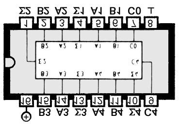
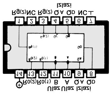
4 BINARY TO BCD DECODERS bit 16 PRIORITY ENCODER to-4-Line to-3-Line to-3 Line 16 MISCELLANEOUS DECODERS 7443 Excess 3 to Decimal Excess 3-Gray to Decimal Segment to BCD Decoder Key Encoder Key Encoder 20 DIVIDERS bit Programmable bit Programmable bit Programmable 16 NON-INVERTING BUS/LINE DRIVERS bit bit x4-bit x4-bit bit with Enable bit with Freigabe bit with Enable 20 INVERTING BUS/LINE DRIVERS x4-bit Inverter/Driver bit bit 20 NON-INVERTING BUS TRANCEIVER bit Bidirectional bit Bidirectional bit with Reg.-Bidirectional bit with Reg.-Bidirectional bit Bidirectional bit Bidirectional bit with Register-Bidirectional bit with Register-Bidirectional 24 INVERTING BUS TRANCEIVER bit Bidirectional bit with Register-Bidirectional bit Bidirectional bit Bidirectional 20 MEMORY PARTS 7484 SRAM 16x1-bit SRAM 16x4-bit SRAM 4x4-bit SRAM 8x2-bit SRAM 16x4-bit PROM 256x4-bit PROM 256x8-bit SRAM 4x4-bit 16 MISCELLANEOUS x Current Sensor x250Ohm Line Driver x250Ohm Line Driver Phase Lock Loop Filter LCD Controller Digit-BCD LED Display Driver Digit Counter with 7-Segment Driver Digit Counter with 7-Segment Driver x Analog Switch Phase Lock Loop x Inverter Lewel Shifter Prescaler/Frequency Divider x Analog Switch x Analog Switch x BCD Counter x Precision Monostabile Multivibrator
5 7400 X X X X X X X 7401 X X X 7402 X X X X X 7403 X X X 7404 X X X X X X 7405 X X 7406 X X 7407 X X 7408 X X X X X 7409 X 7410 X X X X X 7411 X X X 7412 X 7413 X 7414 X X X X X 7415 X 7416 X 7417 X 7418 X 7419 X 7420 X X X 7421 X X X 7422 X 7423 X 7424 X 7425 X 7426 X 7427 X X 7428 X 7430 X X 7432 X X X X X 7433 X 7436 X 7437 X 7438 X X X 7439 X 7440 X X 7441 X 7442 X X X X 7443 X X 7444 X 7445 X 7446 X 7447 X X 7448 X X 7449 X 7450 X 7451 X X 7453 X 7454 X X 7455 X 7456 X 7457 X X 7463 X 7468 X 7469 X 7470 X 7472 X 7473 X X X X X 7474 X X X X X X 7475 X X X X 7476 X X X 7477 X 7478 X 7480 X 7482 X 7483 X X 7484 X 7485 X X X X 7486 X X X X 7489 X 7490 X X 7491 X 7492 X 7493 X X X X 7494 X 7495 X 7496 X 7497 X X X X X X X X X X X X X X X X X X X X X X X X X X X X X X X X X X X X X X X X X X X X X X X X X X X X X X X X X X X X X X X X X X X X X X 194
6 74155 X X X X X X X X X X X X X X X X X X X X X X X X X X X X X X X X X X X X X X X X X X X X X X X X X X X X X X X X X X X X X X X X X X X X X X X X X X X X X X X X X X X X X X X X X X X X X X X X X X X X X X X X X X X X X X X X X X X X X X X X X X X X X X X X X X X X X X X X X X X X X X X X X X X X X X X X X X X X X X X X X X X X X X X X X X X X X X X X X X X X X X X X X X X X X X X X X X X X X X X X X X X X X X X X X X X X X X X X X X X 195
7 74563 X X X X X X X X X X X X X X X X X X X X X X X X X X X X X X X X X X X X X X X X X X X X * * X X X X X X X X X X X X X X X X X X X X X X X X X X X X X X X X X X X X X X X X X X X X X X X X X X X X X X X X X X X X X X X X X X X X X X X X X X X X X X X X X X X X X X X X X X X X X X X X X X X X X X X X X X X X X X X X X X X X X X X X X X X X X 196


8 TTL-s 7400, 7403, , , 7405, 7406, , , ,


9 TTL-s


10 TTL-s
List of the CMOS 4000 series Dual tri-input NOR Gate and Inverter Quad 2-input NOR gate Dual 4-input NOR gate
 List of the CMOS 4000 series 4000 - Dual tri-input NOR Gate and Inverter 4001 - Quad 2-input NOR gate 4002 - Dual 4-input NOR gate 4006-18 stage Shift register 4007 - Dual Complementary Pair Plus Inverter
EE Chip list. Page 1
 Chip # Description 7400 Quadruple 2-Input Positive NANDS 7401 Quadruple 2-Input Positive NAND with Open-Collector Outputs 7402 Quadruple 2-input Positive NOR 7403 Quadruple 2-Intput Positive NAND with
ARCADE IC-LISTE Stand:
 JAMMA CONNECTOR SCART CONNECTOR W. Robel Seite 1 von 36 08.05.2018 AUTOMATEN - TAB HELLOMAT W. Robel Seite 2 von 36 08.05.2018 HELLOMAT W. Robel Seite 3 von 36 08.05.2018 Adp Gauselmann TV Ideal W. Robel
Integrated Circuits 7
 7 IC Test Clip Series For temporary connections to DIP package components Heavy-duty spring loaded hinge provides positive contact 20 AWG insulated gold contacts Color: white 22103 Part No. Product No.
SIGNETICS INTEGRATED CIRCUITS Low Power Schottky TTL 54LS00-74LS00 Series. Supply Current/typmA Delay/typns Quad 2-Input NAND Gate 54LS00/C,D
 SIGNETICS INTEGRATED CIRCUITS Low Power Schottky TTL 54LS00-74LS00 Series Rating Value Unit Voltage - V CC +7.0 V Input Voltage Range - V I -0.5 to +7.0 V Output Voltage - V out +5.5 V Operating Temperature
Massachusetts Institute of Technology Department of Electrical Engineering and Computer Science
 Massachusetts Institute of Technology Department of Electrical Engineering and Computer Science 6.111 - Introductory Digital Systems Laboratory Project Resources Project resources are allocated on a per
Tribhuvan University Institute of Science and Technology Bachelor of Science in Computer Science and Information Technology
 Tribhuvan University Institute of Science and Technology Bachelor of Science in Computer Science and Information Technology Course Title: Digital Logic Full Marks: 60 + 0 + 0 Course No.: CSC Pass Marks:
MODU LE DAY. Class-A, B, AB and C amplifiers - basic concepts, power, efficiency Basic concepts of Feedback and Oscillation. Day 1
 DAY MODU LE TOPIC QUESTIONS Day 1 Day 2 Day 3 Day 4 I Class-A, B, AB and C amplifiers - basic concepts, power, efficiency Basic concepts of Feedback and Oscillation Phase Shift Wein Bridge oscillators.
Bachelor Level/ First Year/ Second Semester/ Science Full Marks: 60 Computer Science and Information Technology (CSc. 151) Pass Marks: 24
 Pass Marks: 24") 2065 Computer Science and Information Technology (CSc. 151) Pass Marks: 24 Time: 3 hours. Candidates are required to give their answers in their own words as for as practicable. Attempt any TWO questions:
2065 Computer Science and Information Technology (CSc. 151) Pass Marks: 24 Time: 3 hours. Candidates are required to give their answers in their own words as for as practicable. Attempt any TWO questions:
MODULAR DIGITAL ELECTRONICS TRAINING SYSTEM
 MODULAR DIGITAL ELECTRONICS TRAINING SYSTEM MDETS UCTECH's Modular Digital Electronics Training System is a modular course covering the fundamentals, concepts, theory and applications of digital electronics.
DIGITAL ELECTRONICS MCQs
 DIGITAL ELECTRONICS MCQs 1. A 8-bit serial in / parallel out shift register contains the value 8, clock signal(s) will be required to shift the value completely out of the register. A. 1 B. 2 C. 4 D. 8
Date: Author: New: Revision: x SAULT COLLEGE OF APPLIED ARTS & TECHNOLOGY SAULT STE. MARIE, ONTARIO ELN TWO
 SAULT COLLEGE OF APPLIED ARTS & TECHNOLOGY SAULT STE. MARIE, ONTARIO COURSE OUTLINE Course Title: DIGITAL ELECTRONICS Code No.: ELN 107-5 Program: ELECTRICAL/ELECTRONIC TECHNICIAN Semester: TWO Date: AUGUST
VU Mobile Powered by S NO Group
 Question No: 1 ( Marks: 1 ) - Please choose one A 8-bit serial in / parallel out shift register contains the value 8, clock signal(s) will be required to shift the value completely out of the register.
4.S-[F] SU-02 June All Syllabus Science Faculty B.Sc. II Yr. Instrumentation Practice [Sem.III & IV] S.Lot
![4.S-[F] SU-02 June All Syllabus Science Faculty B.Sc. II Yr. Instrumentation Practice [Sem.III & IV] S.Lot](/thumbs/90/103282534.jpg "4.S-[F] SU-02 June All Syllabus Science Faculty B.Sc. II Yr. Instrumentation Practice [Sem.III & IV] S.Lot") [Sem.III & IV] S.Lot. - 1 - [Sem.III & IV] S.Lot. - 2 - [Sem.III & IV] S.Lot. - 3 - Syllabus B.Sc. ( Instrumentation Practice ) Second Year ( Third and Forth Semester ) ( Effective from June 2014 ) [Sem.III
[Sem.III & IV] S.Lot. - 1 - [Sem.III & IV] S.Lot. - 2 - [Sem.III & IV] S.Lot. - 3 - Syllabus B.Sc. ( Instrumentation Practice ) Second Year ( Third and Forth Semester ) ( Effective from June 2014 ) [Sem.III
MUHAMMAD NAEEM LATIF MCS 3 RD SEMESTER KHANEWAL
 1. A stage in a shift register consists of (a) a latch (b) a flip-flop (c) a byte of storage (d) from bits of storage 2. To serially shift a byte of data into a shift register, there must be (a) one click
Minnesota State College Southeast
 ELEC 2211: Digital Electronics II A. COURSE DESCRIPTION Credits: 4 Lecture Hours/Week: 2 Lab Hours/Week: 4 OJT Hours/Week: *.* Prerequisites: None Corequisites: None MnTC Goals: None Minnesota State College
TEST-3 (DIGITAL ELECTRONICS)-(EECTRONIC)
-(EECTRONIC)") 1 TEST-3 (DIGITAL ELECTRONICS)-(EECTRONIC) Q.1 The flip-flip circuit is. a) Unstable b) multistable c) Monostable d) bitable Q.2 A digital counter consists of a group of a) Flip-flop b) half adders c)
1 TEST-3 (DIGITAL ELECTRONICS)-(EECTRONIC) Q.1 The flip-flip circuit is. a) Unstable b) multistable c) Monostable d) bitable Q.2 A digital counter consists of a group of a) Flip-flop b) half adders c)
TIME SCHEDULE. MODULE TOPICS PERIODS 1 Number system & Boolean algebra 17 Test I 1 2 Logic families &Combinational logic
 COURSE TITLE : DIGITAL INSTRUMENTS PRINCIPLE COURSE CODE : 3075 COURSE CATEGORY : B PERIODS/WEEK : 4 PERIODS/SEMESTER : 72 CREDITS : 4 TIME SCHEDULE MODULE TOPICS PERIODS 1 Number system & Boolean algebra
1. Convert the decimal number to binary, octal, and hexadecimal.
 1. Convert the decimal number 435.64 to binary, octal, and hexadecimal. 2. Part A. Convert the circuit below into NAND gates. Insert or remove inverters as necessary. Part B. What is the propagation delay
Counter dan Register
 Counter dan Register Introduction Circuits for counting events are frequently used in computers and other digital systems. Since a counter circuit must remember its past states, it has to possess memory.
Find the equivalent decimal value for the given value Other number system to decimal ( Sample)
") VELAMMAL COLLEGE OF ENGINEERING AND TECHNOLOGY, MADURAI 65 009 Department of Information Technology Model Exam-II-Question bank PART A (Answer for all Questions) (8 X = 6) K CO Marks Find the equivalent
VELAMMAL COLLEGE OF ENGINEERING AND TECHNOLOGY, MADURAI 65 009 Department of Information Technology Model Exam-II-Question bank PART A (Answer for all Questions) (8 X = 6) K CO Marks Find the equivalent
R13 SET - 1 '' ''' '' ' '''' Code No: RT21053
 SET - 1 1. a) What are the characteristics of 2 s complement numbers? b) State the purpose of reducing the switching functions to minimal form. c) Define half adder. d) What are the basic operations in
Chapter 2. Digital Circuits
 Chapter 2. Digital Circuits Logic gates Flip-flops FF registers IC registers Data bus Encoders/Decoders Multiplexers Troubleshooting digital circuits Most contents of this chapter were covered in 88-217
DIGITAL FUNDAMENTALS
 DIGITAL FUNDAMENTALS A SYSTEMS APPROACH THOMAS L. FLOYD PEARSON Boston Columbus Indianapolis New York San Francisco Upper Saddle River Amsterdam Cape Town Dubai London Madrid Milan Munich Paris Montreal
Semester III. Subject Name: Digital Electronics. Subject Code: 09CT0301. Diploma Branches in which this subject is offered: Computer Engineering
 Semester III Subject Name: Digital Electronics Subject Code: 09CT0301 Diploma Branches in which this subject is offered: Objective: The subject aims to prepare the students, To understand the basic of
PHYSICS 5620 LAB 9 Basic Digital Circuits and Flip-Flops
 PHYSICS 5620 LAB 9 Basic Digital Circuits and Flip-Flops Objective Construct a two-bit binary decoder. Study multiplexers (MUX) and demultiplexers (DEMUX). Construct an RS flip-flop from discrete gates.
SAULT COLLEGE OF APPLIED ARTS & TECHNOLOGY SAULT STE. MARIE, ONTARIO LOGIC & SWITCHING CIRCUITS NON-SEMESTERED TECHNICIAN PROGRAM
 SAULT COLLEGE OF APPLED ARTS & TECHNOLOGY SAULT STE. MARE, ONTARO COURSE OUTLNE Course Title: LOGC & SWTCHNG CRCUTS Code No.: ELN 207 Program: Semester: Date: Author: NON-SEMESTERED TECHNCAN PROGRAM THREE
R13. II B. Tech I Semester Regular Examinations, Jan DIGITAL LOGIC DESIGN (Com. to CSE, IT) PART-A
 PART-A") SET - 1 Note: Question Paper consists of two parts (Part-A and Part-B) Answer ALL the question in Part-A Answer any THREE Questions from Part-B a) What are the characteristics of 2 s complement numbers?
SET - 1 Note: Question Paper consists of two parts (Part-A and Part-B) Answer ALL the question in Part-A Answer any THREE Questions from Part-B a) What are the characteristics of 2 s complement numbers?
1 Hour Sample Test Papers: Sample Test Paper 1. Roll No.
 6.1.2 Sample Test Papers: Sample Test Paper 1 Roll No. Institute Name: Course Code: EJ/EN/ET/EX/EV/IC/IE/IS/MU/DE/ED/ET/IU Subject: Principles of Digital Techniques Marks: 25 1 Hour 1. All questions are
Theory Lecture Day Topic Practical Day. Week. number systems and their inter-conversion Decimal, Binary. 3rd. 1st. 1st
 Lesson Plan Name of the Faculty : Priyanka Nain Discipline: Electronics & Communication Engg. Semester:5th Subject:DEMP Lesson Plan Duration: 15 Weeks Work Load(Lecture/Practical) per week (In Hours):
DIGITAL SYSTEM DESIGN UNIT I (2 MARKS)
") DIGITAL SYSTEM DESIGN UNIT I (2 MARKS) 1. Convert Binary number (111101100) 2 to Octal equivalent. 2. Convert Binary (1101100010011011) 2 to Hexadecimal equivalent. 3. Simplify the following Boolean function
DIGITAL SYSTEM DESIGN UNIT I (2 MARKS) 1. Convert Binary number (111101100) 2 to Octal equivalent. 2. Convert Binary (1101100010011011) 2 to Hexadecimal equivalent. 3. Simplify the following Boolean function
Operating Manual Ver.1.1
 Johnson Counter Operating Manual Ver.1.1 An ISO 9001 : 2000 company 94-101, Electronic Complex Pardesipura, Indore- 452010, India Tel : 91-731- 2570301/02, 4211100 Fax: 91-731- 2555643 e mail : info@scientech.bz
Solution to Digital Logic )What is the magnitude comparator? Design a logic circuit for 4 bit magnitude comparator and explain it,
What is the magnitude comparator? Design a logic circuit for 4 bit magnitude comparator and explain it,") Solution to Digital Logic -2067 Solution to digital logic 2067 1.)What is the magnitude comparator? Design a logic circuit for 4 bit magnitude comparator and explain it, A Magnitude comparator is a combinational
Solution to Digital Logic -2067 Solution to digital logic 2067 1.)What is the magnitude comparator? Design a logic circuit for 4 bit magnitude comparator and explain it, A Magnitude comparator is a combinational
North Shore Community College
 North Shore Community College Course Number: IEL217 Section: MAL Course Name: Digital Electronics 1 Semester: Credit: 4 Hours: Three hours of Lecture, Two hours Laboratory per week Thursdays 8:00am (See
Introduction. NAND Gate Latch. Digital Logic Design 1 FLIP-FLOP. Digital Logic Design 1
 2007 Introduction BK TP.HCM FLIP-FLOP So far we have seen Combinational Logic The output(s) depends only on the current values of the input variables Here we will look at Sequential Logic circuits The
CS6201 UNIT I PART-A. Develop or build the following Boolean function with NAND gate F(x,y,z)=(1,2,3,5,7).
=(1,2,3,5,7).") VALLIAMMAI ENGINEERING COLLEGE SRM Nagar, Kattankulathur-603203 DEPARTMENT OF COMPUTER SCIENCE AND ENGINEERING Academic Year: 2015-16 BANK - EVEN SEMESTER UNIT I PART-A 1 Find the octal equivalent of hexadecimal
VALLIAMMAI ENGINEERING COLLEGE SRM Nagar, Kattankulathur-603203 DEPARTMENT OF COMPUTER SCIENCE AND ENGINEERING Academic Year: 2015-16 BANK - EVEN SEMESTER UNIT I PART-A 1 Find the octal equivalent of hexadecimal
Chapter 9 MSI Logic Circuits
 Chapter 9 MSI Logic Circuits Chapter 9 Objectives Selected areas covered in this chapter: Analyzing/using decoders & encoders in circuits. Advantages and disadvantages of LEDs and LCDs. Observation/analysis
Registers and Counters
 Registers and Counters Clocked sequential circuit = F/Fs and combinational gates Register Group of flip-flops (share a common clock and capable of storing one bit of information) Consist of a group of
PURBANCHAL UNIVERSITY
 [c] Implement a full adder circuit with a decoder and two OR gates. [4] III SEMESTER FINAL EXAMINATION-2006 Q. [4] [a] What is flip flop? Explain flip flop operating characteristics. [6] [b] Design and
0 0/1 0/1 0/1 0/1 0/1 0/1 0/1 0/1 1 1 Stop bits. 11-bit Serial Data format
 Applications of Shift Registers The major application of a shift register is to convert between parallel and serial data. Shift registers are also used as keyboard encoders. The two applications of the
Digital Networks and Systems Laboratory 2 Basic Digital Building Blocks Time 4 hours
 Digital Networks and Systems Laboratory 2 Basic Digital Building Blocks Time 4 hours Aim To investigate the basic digital circuit building blocks constructed from combinatorial logic or dedicated Integrated
Nirma University Institute of Technology. Electronics and Communication Engineering Department. Course Policy
 Nirma University Institute of Technology Electronics and Communication Engineering Department Course Policy B. Tech Semester - III Academic Year: 2017 Course Code & Name : Credit Details : L T P C 4 2
Combinational vs Sequential
 Combinational vs Sequential inputs X Combinational Circuits outputs Z A combinational circuit: At any time, outputs depends only on inputs Changing inputs changes outputs No regard for previous inputs
Course Plan. Course Articulation Matrix: Mapping of Course Outcomes (COs) with Program Outcomes (POs) PSO-1 PSO-2
 with Program Outcomes (POs) PSO-1 PSO-2") Course Plan Semester: 4 - Semester Year: 2019 Course Title: DIGITAL ELECTRONICS Course Code: EC106 Semester End Examination: 70 Continuous Internal Evaluation: 30 Lesson Plan Author: Ms. CH SRIDEVI Last
Course Plan Semester: 4 - Semester Year: 2019 Course Title: DIGITAL ELECTRONICS Course Code: EC106 Semester End Examination: 70 Continuous Internal Evaluation: 30 Lesson Plan Author: Ms. CH SRIDEVI Last
T e. e available in EIAJ e available in JEDEC and EIAJ e available in wide format e available in standard and. T w. e planned in standard
 CMOS Logic KEY October 1995 Semiconductor Corporation CMOS Logic Advanced CMOS FACT TM (AC) FACT Quiet Series TM (ACQ) FACT (ACT) FACT Quiet Series (ACTQ) FACT FCT VHCVHCT HCHCT T e T e w T w Pw Z eavailable
Registers and Counters
 Registers and Counters Clocked sequential circuit = F/Fs and combinational gates Register Group of flip-flops (share a common clock and capable of storing one bit of information) Consist of a group of
Electrical and Telecommunications Engineering Technology_TCET3122/TC520. NEW YORK CITY COLLEGE OF TECHNOLOGY The City University of New York
 NEW YORK CITY COLLEGE OF TECHNOLOGY The City University of New York DEPARTMENT: SUBJECT CODE AND TITLE: COURSE DESCRIPTION: REQUIRED: Electrical and Telecommunications Engineering Technology TCET 3122/TC
Contents Circuits... 1
 Contents Circuits... 1 Categories of Circuits... 1 Description of the operations of circuits... 2 Classification of Combinational Logic... 2 1. Adder... 3 2. Decoder:... 3 Memory Address Decoder... 5 Encoder...
VeriLab. An introductory lab for using Verilog in digital design (first draft) VeriLab
 VeriLab") VeriLab An introductory lab for using Verilog in digital design (first draft) VeriLab An introductory lab for using Verilog in digital design Verilog is a hardware description language useful for designing
VeriLab An introductory lab for using Verilog in digital design (first draft) VeriLab An introductory lab for using Verilog in digital design Verilog is a hardware description language useful for designing
CS302 Digital Logic Design Solved Objective Midterm Papers For Preparation of Midterm Exam
 CS302 Digital Logic Design Solved Objective Midterm Papers For Preparation of Midterm Exam MIDTERM EXAMINATION Spring 2012 Question No: 1 ( Marks: 1 ) - Please choose one A SOP expression is equal to 1
WINTER 15 EXAMINATION Model Answer
 Important Instructions to examiners: 1) The answers should be examined by key words and not as word-to-word as given in the model answer scheme. 2) The model answer and the answer written by candidate
Operating Manual Ver.1.1
 Event Counter Operating Manual Ver.1.1 An ISO 9001 : 2000 company 94-101, Electronic Complex Pardesipura, Indore- 452010, India Tel : 91-731- 2570301/02, 4211100 Fax: 91-731- 2555643 e mail : info@scientech.bz
[2 credit course- 3 hours per week]
![[2 credit course- 3 hours per week]](/thumbs/94/121292011.jpg "[2 credit course- 3 hours per week]") Syllabus of Applied Electronics for F Y B Sc Semester- 1 (With effect from June 2012) PAPER I: Components and Devices [2 credit course- 3 hours per week] Unit- I : CIRCUIT THEORY [10 Hrs] Introduction;
Syllabus of Applied Electronics for F Y B Sc Semester- 1 (With effect from June 2012) PAPER I: Components and Devices [2 credit course- 3 hours per week] Unit- I : CIRCUIT THEORY [10 Hrs] Introduction;
Logic. Q100 Logic portfolio Continuing to lead the way in automotive logic
 Logic Q100 Logic portfolio Continuing to lead the way in automotive logic 2 Q100 Logic portfolio The operating environment of automobile semiconductor components is much more hostile than that of semiconductors
Serial In/Serial Left/Serial Out Operation
 Shift Registers The need to storage binary data was discussed earlier. In digital circuits multi-bit data has to be stored temporarily until it is processed. A flip-flop is able to store a single binary
TYPICAL QUESTIONS & ANSWERS
 DIGITALS ELECTRONICS TYPICAL QUESTIONS & ANSWERS OBJECTIVE TYPE QUESTIONS Each Question carries 2 marks. Choose correct or the best alternative in the following: Q.1 The NAND gate output will be low if
Question Bank. Unit 1. Digital Principles, Digital Logic
 Question Bank Unit 1 Digital Principles, Digital Logic 1. Using Karnaugh Map,simplify the following boolean expression and give the implementation of the same using i)nand gates only(sop) ii) NOR gates
RS flip-flop using NOR gate
 RS flip-flop using NOR gate Triggering and triggering methods Triggering : Applying train of pulses, to set or reset the memory cell is known as Triggering. Triggering methods:- There are basically two
TRAINING KITS ON DIGITAL ELECTRONIC EXPERIMENTS. Verify Truth table for TTL IC s AND, NOT, & NAND GATES
 TRAINING KITS ON DIGITAL ELECTRONIC EXPERIMENTS CEE 2800 Basic Logic Gates using TTL IC's (7 in 1) To verify the truth table For TTL AND, OR. NOT, NAND,NOR, EX-OR, & EX-NOR Gates. Instrument comprises
Vignana Bharathi Institute of Technology UNIT 4 DLD
 DLD UNIT IV Synchronous Sequential Circuits, Latches, Flip-flops, analysis of clocked sequential circuits, Registers, Shift registers, Ripple counters, Synchronous counters, other counters. Asynchronous
WINTER 14 EXAMINATION
 Subject Code: 17320 WINTER 14 EXAMINATION Model Answer Important Instructions to examiners: 1) The answers should be examined by key words and not as word-to-word as given in the model answer scheme. 2)
MODULE 3. Combinational & Sequential logic
 MODULE 3 Combinational & Sequential logic Combinational Logic Introduction Logic circuit may be classified into two categories. Combinational logic circuits 2. Sequential logic circuits A combinational
QUICK GUIDE COMPUTER LOGICAL ORGANIZATION - OVERVIEW
 QUICK GUIDE http://www.tutorialspoint.com/computer_logical_organization/computer_logical_organization_quick_guide.htm COMPUTER LOGICAL ORGANIZATION - OVERVIEW Copyright tutorialspoint.com In the modern
Scanned by CamScanner
 NAVEEN RAJA VELCHURI DSD & Digital IC Applications Example: 2-bit asynchronous up counter: The 2-bit Asynchronous counter requires two flip-flops. Both flip-flop inputs are connected to logic 1, and initially
YEDITEPE UNIVERSITY DEPARTMENT OF COMPUTER ENGINEERING. EXPERIMENT VIII: FLIP-FLOPS, COUNTERS 2014 Fall
 YEDITEPE UNIVERSITY DEPARTMENT OF COMPUTER ENGINEERING EXPERIMENT VIII: FLIP-FLOPS, COUNTERS 2014 Fall Objective: - Dealing with the operation of simple sequential devices. Learning invalid condition in
Come and join us at WebLyceum
 Come and join us at WebLyceum For Past Papers, Quiz, Assignments, GDBs, Video Lectures etc Go to http://www.weblyceum.com and click Register In Case of any Problem Contact Administrators Rana Muhammad
RS flip-flop using NOR gate
 RS flip-flop using NOR gate Triggering and triggering methods Triggering : Applying train of pulses, to set or reset the memory cell is known as Triggering. Triggering methods:- There are basically two
Subject : EE6301 DIGITAL LOGIC CIRCUITS
 QUESTION BANK Programme : BE Subject : Semester / Branch : III/EEE UNIT 1 NUMBER SYSTEMS AND DIGITAL LOGIC FAMILIES Review of number systems, binary codes, error detection and correction codes (Parity
CSE115: Digital Design Lecture 23: Latches & Flip-Flops
 Faculty of Engineering CSE115: Digital Design Lecture 23: Latches & Flip-Flops Sections 7.1-7.2 Suggested Reading A Generic Digital Processor Building Blocks for Digital Architectures INPUT - OUTPUT Interconnect:
EKT 121/4 ELEKTRONIK DIGIT 1
 EKT 121/4 ELEKTRONIK DIGIT 1 Kolej Universiti Kejuruteraan Utara Malaysia Bistable Storage Devices and Related Devices Introduction Latches and flip-flops are the basic single-bit memory elements used
Logic Design. Flip Flops, Registers and Counters
 Logic Design Flip Flops, Registers and Counters Introduction Combinational circuits: value of each output depends only on the values of inputs Sequential Circuits: values of outputs depend on inputs and
NH 67, Karur Trichy Highways, Puliyur C.F, Karur District UNIT-III SEQUENTIAL CIRCUITS
 NH 67, Karur Trichy Highways, Puliyur C.F, 639 114 Karur District DEPARTMENT OF ELETRONICS AND COMMUNICATION ENGINEERING COURSE NOTES SUBJECT: DIGITAL ELECTRONICS CLASS: II YEAR ECE SUBJECT CODE: EC2203
Asynchronous (Ripple) Counters
 Counters") Circuits for counting events are frequently used in computers and other digital systems. Since a counter circuit must remember its past states, it has to possess memory. The chapter about flip-flops introduced
Circuits for counting events are frequently used in computers and other digital systems. Since a counter circuit must remember its past states, it has to possess memory. The chapter about flip-flops introduced
Helping Material of CS302
 ABEL : Advanced Boolean Expression Language; a software compiler language for SPLD programming; a type of hardware description language (HDL) Adder : A digital circuit which forms the sum and carry of
Department of Computer Science and Engineering Question Bank- Even Semester:
 Department of Computer Science and Engineering Question Bank- Even Semester: 2014-2015 CS6201& DIGITAL PRINCIPLES AND SYSTEM DESIGN (Common to IT & CSE, Regulation 2013) UNIT-I 1. Convert the following
Sequential Digital Design. Laboratory Manual. Experiment #7. Counters
 The Islamic University of Gaza Engineering Faculty Department of Computer Engineering Spring 2018 ECOM 2022 Khaleel I. Shaheen Sequential Digital Design Laboratory Manual Experiment #7 Counters Objectives
Flip-Flops and Related Devices. Wen-Hung Liao, Ph.D. 4/11/2001
 Flip-Flops and Related Devices Wen-Hung Liao, Ph.D. 4/11/2001 Objectives Recognize the various IEEE/ANSI flip-flop symbols. Use state transition diagrams to describe counter operation. Use flip-flops in
UNIVERSITI TEKNOLOGI MALAYSIA
 SULIT Faculty of Computing UNIVERSITI TEKNOLOGI MALAYSIA FINAL EXAMINATION SEMESTER I, 2016 / 2017 SUBJECT CODE : SUBJECT NAME : SECTION : TIME : DATE/DAY : VENUES : INSTRUCTIONS : Answer all questions
Operating Manual Ver.1.1
 Keyboard Encoder Operating Manual Ver.1.1 An ISO 9001 : 2000 company 94-101, Electronic Complex Pardesipura, Indore- 452010, India Tel : 91-731- 2570301/02, 4211100 Fax: 91-731- 2555643 e mail : info@scientech.bz
Rangkaian Sekuensial. Flip-flop
 Rangkaian Sekuensial Rangkaian Sekuensial Flip-flop Combinational versus Sequential Functions Logic functions are categorized as being either combinational (sometimes referred to as combinatorial) or sequential.
Digital Fundamentals: A Systems Approach
 Digital Fundamentals: A Systems Approach Latches, Flip-Flops, and Timers Chapter 6 Traffic Signal Control Traffic Signal Control: State Diagram Traffic Signal Control: Block Diagram Traffic Signal Control:
AIM: To study and verify the truth table of logic gates
 EXPERIMENT: 1- LOGIC GATES AIM: To study and verify the truth table of logic gates LEARNING OBJECTIVE: Identify various Logic gates and their output. COMPONENTS REQUIRED: KL-31001 Digital Logic Lab( Main
Lecture 12. Amirali Baniasadi
 CENG 24 Digital Design Lecture 2 Amirali Baniasadi amirali@ece.uvic.ca This Lecture Chapter 6: Registers and Counters 2 Registers Sequential circuits are classified based in their function, e.g., registers.
Digital Fundamentals: A Systems Approach
 Digital Fundamentals: A Systems Approach Counters Chapter 8 A System: Digital Clock Digital Clock: Counter Logic Diagram Digital Clock: Hours Counter & Decoders Finite State Machines Moore machine: One
Microprocessor Design
 Microprocessor Design Principles and Practices With VHDL Enoch O. Hwang Brooks / Cole 2004 To my wife and children Windy, Jonathan and Michelle Contents 1. Designing a Microprocessor... 2 1.1 Overview
MAHARASHTRA STATE BOARD OF TECHNICAL EDUCATION (Autonomous) (ISO/IEC Certified) WINTER 2018 EXAMINATION MODEL ANSWER
 (ISO/IEC Certified) WINTER 2018 EXAMINATION MODEL ANSWER") Important Instructions to examiners: 1) The answers should be examined by key words and not as word-to-word as given in themodel answer scheme. 2) The model answer and the answer written by candidate may
Important Instructions to examiners: 1) The answers should be examined by key words and not as word-to-word as given in themodel answer scheme. 2) The model answer and the answer written by candidate may
 UNIT 1 NUMBER SYSTEMS AND DIGITAL LOGIC FAMILIES 1. Briefly explain the stream lined method of converting binary to decimal number with example. 2. Give the Gray code for the binary number (111) 2. 3.
LATCHES & FLIP-FLOP. Chapter 7
 LATCHES & FLIP-FLOP Chapter 7 INTRODUCTION Latch and flip flops are categorized as bistable devices which have two stable states,called SET and RESET. They can retain either of this states indefinitely
Chapter 6 Registers and Counters
 EEA051 - Digital Logic 數位邏輯 Chapter 6 Registers and Counters 吳俊興國立高雄大學資訊工程學系 January 2006 Chapter 6 Registers and Counters 6-1 Registers 6-2 Shift Registers 6-3 Ripple Counters 6-4 Synchronous Counters
Counters
 Counters A counter is the most versatile and useful subsystems in the digital system. A counter driven by a clock can be used to count the number of clock cycles. Since clock pulses occur at known intervals,
Sri Vidya College of Engineering And Technology. Virudhunagar Department of Electrical and Electronics Engineering
 Sri Vidya College of Engineering And Technology Virudhunagar 626 005 Department of Electrical and Electronics Engineering Year/ Semester/ Class : II/ III/ EEE Academic Year: 2017-2018 Subject Code/ Name:
Name Of The Experiment: Sequential circuit design Latch, Flip-flop and Registers
 EEE 304 Experiment No. 07 Name Of The Experiment: Sequential circuit design Latch, Flip-flop and Registers Important: Submit your Prelab at the beginning of the lab. Prelab 1: Construct a S-R Latch and
LESSON PLAN. Sub Code: EE2255 Sub Name: DIGITAL LOGIC CIRCUITS Unit: I Branch: EEE Semester: IV
 Unit: I Branch: EEE Semester: IV Page 1 of 6 Unit I Syllabus: BOOLEAN ALGEBRA AND COMBINATIONAL CIRCUITS 9 Boolean algebra: De-Morgan s theorem, switching functions and simplification using K-maps & Quine
CS302 Glossary. address : The location of a given storage cell or group of cells in a memory; a unique memory location containing one byte.
 CS302 Glossary ABEL Advanced Boolean Expression Language; a software compiler language for SPLD programming; a type of hardware description language (HDL) Adder A digital circuit which forms the sum and
Digital Systems Laboratory 3 Counters & Registers Time 4 hours
 Digital Systems Laboratory 3 Counters & Registers Time 4 hours Aim: To investigate the counters and registers constructed from flip-flops. Introduction: In the previous module, you have learnt D, S-R,
DIGITAL SYSTEM FUNDAMENTALS (ECE421) DIGITAL ELECTRONICS FUNDAMENTAL (ECE422) COUNTERS
 DIGITAL ELECTRONICS FUNDAMENTAL (ECE422) COUNTERS") COURSE / CODE DIGITAL SYSTEM FUNDAMENTALS (ECE421) DIGITAL ELECTRONICS FUNDAMENTAL (ECE422) COUNTERS One common requirement in digital circuits is counting, both forward and backward. Digital clocks and
COURSE / CODE DIGITAL SYSTEM FUNDAMENTALS (ECE421) DIGITAL ELECTRONICS FUNDAMENTAL (ECE422) COUNTERS One common requirement in digital circuits is counting, both forward and backward. Digital clocks and
Universal Asynchronous Receiver- Transmitter (UART)
") Universal Asynchronous Receiver- Transmitter (UART) (UART) Block Diagram Four-Bit Bidirectional Shift Register Shift Register Counters Shift registers can form useful counters by recirculating a pattern
Universal Asynchronous Receiver- Transmitter (UART) (UART) Block Diagram Four-Bit Bidirectional Shift Register Shift Register Counters Shift registers can form useful counters by recirculating a pattern
I B.SC (INFORMATION TECHNOLOGY) [ ] Semester II CORE : DIGITAL COMPUTER FUNDAMENTALS - 212B Multiple Choice Questions.
![I B.SC (INFORMATION TECHNOLOGY) [ ] Semester II CORE : DIGITAL COMPUTER FUNDAMENTALS - 212B Multiple Choice Questions.](/thumbs/95/125864820.jpg "I B.SC (INFORMATION TECHNOLOGY) [ ] Semester II CORE : DIGITAL COMPUTER FUNDAMENTALS - 212B Multiple Choice Questions.") Dr.G.R.Damodaran College of Science (Autonomous, affiliated to the Bharathiar University, recognized by the UGC)Re-accredited at the 'A' Grade Level by the NAAC and ISO 9001:2008 Certified CRISL rated
Dr.G.R.Damodaran College of Science (Autonomous, affiliated to the Bharathiar University, recognized by the UGC)Re-accredited at the 'A' Grade Level by the NAAC and ISO 9001:2008 Certified CRISL rated
For Teacher's Use Only Q Total No. Marks. Q No Q No Q No
 FINALTERM EXAMINATION Spring 2010 CS302- Digital Logic Design (Session - 4) Time: 90 min Marks: 58 For Teacher's Use Only Q 1 2 3 4 5 6 7 8 Total No. Marks Q No. 9 10 11 12 13 14 15 16 Marks Q No. 17 18
DHANALAKSHMI SRINIVASAN INSTITUTE OF RESEARCH AND TECHNOLOGY CS6201-DIGITAL PRINCIPLE AND SYSTEM DESIGN. I Year/ II Sem PART-A TWO MARKS UNIT-I
 DHANALAKSHMI SRINIVASAN INSTITUTE OF RESEARCH AND TECHNOLOGY CS6201-DIGITAL PRINCIPLE AND SYSTEM DESIGN I Year/ II Sem PART-A TWO MARKS UNIT-I BOOLEAN ALGEBRA AND LOGIC GATES 1) What are basic properties