Micro-spectrometer C12666MA. Finger-tip size, ultra-compact spectrometer head integrating MEMS and image sensor technologies.
|
|
|
- Arleen Miller
- 6 years ago
- Views:
Transcription
.")
1 Finger-tip size, ultra-compact spectrometer head integrating MEMS and technologies The is an ultra-compact (Finger-tip size) spectrometer head developed based on our MEMS and technologies. The adoption of a newly designed optical system has achieved a remarkably small size, less than half the volume of the previous mini-spectrometer MS series (C9MA-01). In addition, the employment of hermetic packaging has improved humidity resistance. This product is suitable for integration into a variety of devices, such as integration into printers and hand-held color monitoring devices that require color management. It is also suitable for applications that collaborate with portable devices, such as smartphones and tablets. Features Applications Finger-tip size: mm Weight: 5 g Spectral response range: 340 to 70 nm Spectral resolution: 15 nm max. Hermetic package: High reliability against humidity Installation into mobile measurement equipment Wavelength conversion factor* 1 is listed on final inspection sheet Color monitoring for printers and printing machines Testers for lights and LEDs Color adjustment of various large size displays Water quality control monitors and other environment measuring instruments Measuring instruments that use portable devices such as smartphones and tablets *1: A conversion factor for converting the pixel number into a wavelength. A calculation factor for converting the A/D converted count into the input light level is not provided. Optical characteristics Parameter Value Unit Spectral response range 340 to 70 nm Spectral resolution (FWHM) 15 max. nm Wavelength reproducibility* to +0.5 nm Wavelength temperature dependence -0.1 to +0.1 nm/ C Spectral stray light* 3-25 db *2: Measured under constant light input conditions *3: Spectral stray light = log (Tl/Th) Th: count measured when light at a certain wavelength is input Tl: count measured at a wavelength 40 nm longer or shorter than the input light wavelength Electrical characteristics Parameter Min. Typ. Max. Unit Supply voltage V Power consumption mw Video rate khz Output impedance * 4 - Ω *4: An increase in the current consumption at the video output terminal also increases the chip temperature and so causes the dark current to rise. To avoid this, connect a buffer amplifier for impedance conversion to the video output terminal so that the current flow is minimized. As the buffer amplifier, use a JFET or CMOS input operational amplifier of optical input impedance. 1
 with a slit - Number of pixels 256 pixels Pixel size (H V) 12.")

2 Structure Parameter Specification Unit Dimensions (W D H) mm Weight 5 g Slit* 5 (H V) μm NA* Image sensor (H V) with a slit - Number of pixels 256 pixels Pixel size (H V) μm *5: Entrance slit aperture size *6: Numeric aperture (solid angle) Absolute maximum ratings Parameter Value Unit Operating temperature* 7 +5 to +50 C Storage temperature* 7-20 to +70 C *7: No dew condensation When there is a temperature difference between a product and the surrounding area in high humidity environment, dew condensation may occur on the product surface. Dew condensation on the product may cause deterioration in characteristics and reliability. Note: Exceeding the absolute maximum ratings even momentarily may cause a drop in product quality. Always be sure to use the product within the absolute maximum ratings. Optical component layout Besides a CMOS chip integrated with an optical slit by etching technology, the employs a reflective concave blazed grating formed by nanoimprint. In addition, the glass used in the light path of the previous C9MA-01 is not used in the, making it extremely compact. Previous product C9MA-01 Structure High-sensitivity Incident light image sensor with slit Input slit Hollow with a slit [Incident light side (back of chip)] Slit Reflective concave blazed grating Grating chip KACCC0757EB CMOS chip 2
3 Spectral response (typical example) 0 (Ta=25 C) Spectral resolution vs. wavelength (typical example) 14 (Ta=25 C) 12 0 Relative sensitivity (%) Spectral resolution (nm) Wavelength (nm) Wavelength (nm) KACCB0350EB KACCB0351EA Linearity (typical example) Dark output vs. ambient temperature (typical example) A/D output (using C14465-, low gain) Typical example of A/D output Ideal A/D output Difference between ideal value and typical example Difference between ideal value and typical example (%) A/D output (averaged over all pixels) (using C14465-, integration time s, low gain) Integration time (ms) Ambient temperature ( C) A/D output is the output with dark output is subtracted when light is input. The difference between the ideal value and typical example contains a measurement error. The smaller the A/D output, the larger the measurement error. A/D output is the sum of the sensor and circuit offset outputs and the sensor dark output. KACCB0354EC KACCB0352EB 3
4 Measurable incident light level Incident light level* (W) * Input spot diameter: 00 μm (λ=550 nm) KACCB354EA Recommended driver circuit example A/D converter etc Timing generator Analog arithmetic circuit * (subtraction, amplification, etc.) * Use as needed Digital buffer - + Vdd Gain CLK ST EOS Vdd 9 Gain 4 CLK 7 ST EOS 1 Vdd 5 Case 3 GND 2 Video KACCC075EB Precautions The packaging of is electrically conductive, so be careful when designing the circuit to avoid short circuit caused by contact with a circuit pattern. If external force is repeatedly applied to the lead pins, this may damage the lead pins. To prevent damage due to soldering, be careful of the soldering temperature and time. As a general guide, finish soldering within 3.5 seconds at 350 C or less when soldering by hand, or within seconds at 260 C or less when using a solder bath. 4
5 Dimensional outline (unit: mm, tolerance unless otherwise noted: ±0.2) Slit ϕ3.2-0 [Top view] Index mark Slit position 1.53 [Side view] [Bottom view] 3.3 ± ± ϕ1.4 ± Vdd Video GND CLK Case NC ST NC Gain EOS KACCA0336EB Pin connections Make electrical connections to an external circuit using leads. Pin no. Symbol Name I/O Description 1 Vdd Supply voltage I Image sensor power supply: 5 V 2 Video Video output O Video output signal 3 GND Ground - Sensor ground 4 CLK Clock pulse I Sensor scan sync signal 5 Case Case - Case connection terminal 6 NC - No connection 7 ST Start pulse I Start pulse NC - No connection 9 Gain Gain I Image sensor: Gain setting EOS End of scan O Sensor scan end signal Note: Pin no. 9 is pulled up internally to Vdd via kω. Do not pull-up or pull-down the gain setting using an external circuit. For low gain, leave the pin open or connect to Vdd. For high gain, connect to GND. 5
6 Recommended terminal voltage Internal CMOS specifications Parameter Symbol Min. Typ. Max. Unit Supply voltage Vdd V Gain selection terminal High gain V Gain voltage Low gain Vdd Vdd Vdd V Clock pulse voltage High level Vdd Vdd Vdd V V(CLK) Low level V Start pulse voltage High level Vdd Vdd Vdd V V(ST) Low level V Electrical characteristics [Ta=25 C, Vdd=5 V, V(CLK)=V(ST)=5 V] Parameter Symbol Min. Typ. Max. Unit Clock pulse frequency f(clk) 1-00 khz Power consumption High gain P Low gain mw Electrical and optical characteristics [Ta=25 C, Vdd=5 V, V(CLK)=V(ST)=5 V] Parameter Symbol Min. Typ. Max. Unit Dark current High gain ID Low gain pa Output offset voltage High gain Vo Low gain V Charge amplifier feedback High gain capacitance* Cf Low gain pf Saturation output voltage* 9 High gain Vsat Low gain V Readout noise High gain Nr Low gain mv rms *: Gain=5 V (low gain), Vg=0 V (high gain) *9: Voltage difference relative to Vo 6
7 Timing chart Integration time CLK thw (ST) ST Video TRIG EOS tr(clk) tf(clk) CLK tr(st) tf(st) ST tvd Video KACCC0493EB Parameter Symbol Min. Typ. Max. Unit Start pulse high period thw(st) 30/f(CLK) - - s Start pulse rise/fall times tr(st), tf(st) ns Clock pulse duty ratio % Clock pulse rise/fall times tr(clk), tf(clk) ns Video delay time tvd ns Note: The clock pulse should be set from high to low just once when the start pulse is low. The internal shift register starts operating at this timing. The integration time is determined by the start pulse intervals. However, since the charge integration of each pixel is carried out between the signal readout of that pixel and the next signal readout of the same pixel, the start time of charge integration differs depending on each pixel. In addition, the next start pulse cannot be input until signal readout from all pixels is completed. Video output is 1/4 of the clock pulse frequency. 7
*.")
8 Micro-spectrometer evaluation circuit C (sold separately) The C is a circuit board designed to simply evaluate the characteristics of the micro-spectrometer. The characteristics of the micro-spectrometer can be evaluated using the evaluation software by connecting the micro-spectrometer to a PC with a USB cable A9160 (AB type, sold separately)*. Features Initial evaluation circuit for micro-spectrometer* 11 Wavelength conversion factors of the micro-spectrometer can be input from a PC.* 12 High A/D resolution (16-bit) USB powered *: Compatible OS: Microsoft Windows 7 Professional SP1 (32-bit, 64-bit) Microsoft Windows Professional (32-bit, 64-bit) Microsoft Windows Professional (32-bit, 64-bit) *11: The C is a modified version of the C14465 evaluation circuit for the previous mini-spectrometer MS series (C9MA-01, C1170MA). Only the sensor board has been modified. If you already have the C14465, you only have to purchase the C (the sensor board for micro-spectrometers) to evaluate micro-spectrometers. *12: A typical wavelength conversion factor is entered at the time of shipment of the C To measure a spectrum with higher wavelength accuracy, it is necessary to input the wavelength conversion factor listed in the final inspection sheet that comes with each micro-spectrometer. Note: Microsoft and Windows are registered trademarks of Microsoft Corporation in the United States and/or other countries. Electrical characteristics Parameter Specification Unit Interface USB A/D conversion 16 bit Clock pulse frequency 00 khz Video rate 200 khz Integration time 5 to 000 ms Structure Parameter Specification Unit Applicable spectrometer - Dimensions Control board 0 60 mm Sensor board mm Absolute maximum ratings Parameter Value Unit Operating temperature* to +40 C Storage temperature* to +70 C *13: No dew condensation When there is a temperature difference between a product and the surrounding area in high humidity environment, dew condensation may occur on the product surface. Dew condensation on the product may cause deterioration in characteristics and reliability. Note: Exceeding the absolute maximum ratings even momentarily may cause a drop in product quality. Always be sure to use the product within the absolute maximum ratings.
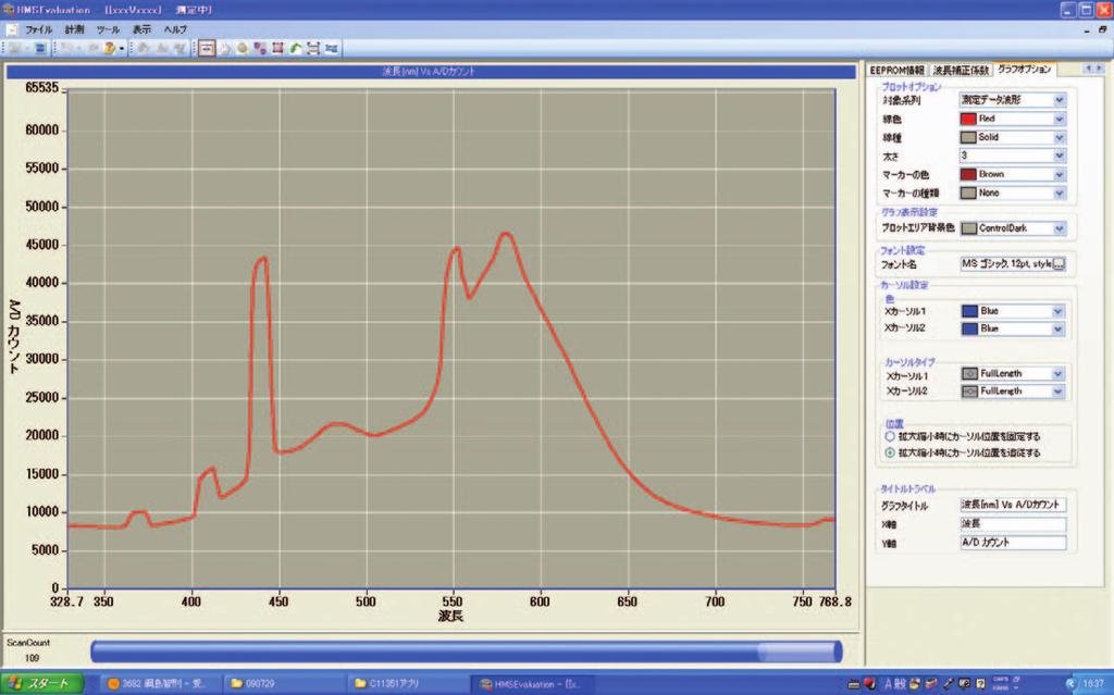


9 Connection example USB cable A9160 (sold separately) Detection source PC Control board Sensor board C Micro-spectrometer (sold separately) Micro-spectrometer evaluation circuit C KACCC0759EC Evaluation software display example 9
10 /micro-spectrometer lineup Type no. C02CA C02CAH C02MD C03CA C03CAH C03MD C11697MB C9404CA C9404CAH C9405CB C11713CA C11714CB C1142GA C9913GC C9914GB C1111GA TM series TG series TG series Type TM-UV/VIS-CCD High sensitivity TM-UV/VIS-CCD High resolution TM-UV/VIS-MOS Wide dynamic range TM-VIS/NIR-CCD High sensitivity TM-VIS/NIR-CCD High resolution TM-VIS/NIR-MOS Wide dynamic range TM-VIS/NIR-MOS-II Trigger-compatible TG-UV-CCD High sensitivity TG-UV-CCD High resolution TG-SWNIR-CCD-II IR-enhanced TG-RAMAN-I High resolution TG-RAMAN-II High resolution TG2-NIR Non-cooled type TG-cooled NIR-I Low noise (cooled type) TG-cooled NIR-II Low noise (cooled type) TG-cooled NIR-III Low noise (cooled type) Spectral response range (nm) to to to to to to to to to 2550 Spectral resolution max. (nm) 6 1* 3 1* 5 (λ=550 to 900 nm) 0.3* 0.3* Image sensor Back-thinned CCD 6 (λ=320 to 900 nm) Back-thinned CCD 1* (λ=320 to 900 nm) High-sensitivity CMOS linear Back-thinned CCD IR-enhanced back-thinned CCD Back-thinned CCD IR-enhanced back-thinned CCD InGaAs linear C13053MA C13054MA C13555MA C107MA C10MA * Typ. TF series RC series TF-SWIR-MOS-II Compact, thin case TF-RAMAN Compact, thin case TF-VIS-MOS-II Compact, thin case RC-VIS-MOS Spectrometer module RC-SWNIR-MOS Spectrometer module 500 to to to to to * 3 9 High-sensitivity IR-enhanced For installation into mobile measuring equipment Type no. C109MA C1MA RC series Type RC-VIS-MOS Spectrometer head RC-SWNIR-MOS Spectrometer head Spectral response range (nm) to to 50 Spectral resolution max. (nm) 9 Image sensor IR-enhanced For installation into mobile measuring equipment (ultra-compact) Type no. C1170MA C120MA MS series Microspectrometer Type MS-SWNIR-MOS Spectrometer head Spectrometer head Spectrometer head Spectral response range (nm) to to to 50 Spectral resolution max. (nm) Image sensor High-sensitivity
11 Related information Precautions Disclaimer Technical information s Information described in this material is current as of November Product specifications are subject to change without prior notice due to improvements or other reasons. This document has been carefully prepared and the information contained is believed to be accurate. In rare cases, however, there may be inaccuracies such as text errors. Before using these products, always contact us for the delivery specification sheet to check the latest specifications. The product warranty is valid for one year after delivery and is limited to product repair or replacement for defects discovered and reported to us within that one year period. However, even if within the warranty period we accept absolutely no liability for any loss caused by natural disasters or improper product use. Copying or reprinting the contents described in this material in whole or in part is prohibited without our prior permission. HAMAMATSU PHOTONICS K.K., Solid State Division Ichino-cho, Higashi-ku, Hamamatsu City, Japan, Telephone: (1) , Fax: (1) U.S.A.: Hamamatsu Corporation: 360 Foothill Road, Bridgewater, N.J. 007, U.S.A., Telephone: (1) , Fax: (1) , usa@hamamatsu.com Germany: Hamamatsu Photonics Deutschland GmbH: Arzbergerstr., D-2211 Herrsching am Ammersee, Germany, Telephone: (49) , Fax: (49) , info@hamamatsu.de France: Hamamatsu Photonics France S.A.R.L.: 19, Rue du Saule Trapu, Parc du Moulin de Massy, 912 Massy Cedex, France, Telephone: 33-(1) , Fax: 33-(1) , infos@hamamatsu.fr United Kingdom: Hamamatsu Photonics UK Limited: 2 Howard Court, Tewin Road, Welwyn Garden City, Hertfordshire AL7 1BW, United Kingdom, Telephone: (44) , Fax: (44) , info@hamamatsu.co.uk North Europe: Hamamatsu Photonics Norden AB: Torshamnsgatan Kista, Sweden, Telephone: (46) , Fax: (46) , info@hamamatsu.se Italy: Hamamatsu Photonics Italia S.r.l.: Strada della Moia, 1 int. 6, Arese (Milano), Italy, Telephone: (39) , Fax: (39) , info@hamamatsu.it China: Hamamatsu Photonics (China) Co., Ltd.: B1201, Jiaming Center, No.27 Dongsanhuan Beilu, Chaoyang District, Beijing 0020, China, Telephone: (6) , Fax: (6) , hpc@hamamatsu.com.cn Taiwan: Hamamatsu Photonics Taiwan Co., Ltd.: F-3, No. 15, Section2, Gongdao 5th Road, East District, Hsinchu, 300, Taiwan R.O.C. Telephone: (6) , Fax: (6) , info@tw.hpk.co.jp 11 Cat. No. KACC1216E09 Nov DN
Micro-spectrometer C12666MA. Finger-tip size, ultra-compact spectrometer head integrating MEMS and image sensor technologies.
 Finger-tip size, ultra-compact spectrometer head integrating MEMS and technologies The is an ultra-compact (Finger-tip size) spectrometer head developed based on our MEMS and technologies. The adoption
Mini-spectrometers. MS series. Ultra-compact mini-spectrometer integrating MEMS and image sensor technologies.
 s MS series C9MA-01 C1170MA Ultra-compact mini-spectrometer integrating MEMS and technologies The MS series are thumb-sized (27.6 16. 13 mm) spectrometer heads developed for installation into mobile measurement
TM series TM-UV/VIS-MOS
 C12MD C13MD For UV to near IR, integrating optical system, and circuit mini-spectrometers are polychromators integrated with optical elements, an and a driver circuit. Two models are available: C12MD (TM-UV/VIS-MOS)
Mini-spectrometer. TF series. Compact and thin, built-in high-sensitivity CMOS image sensor for Raman spectroscopy C14214MA. Applications.
 TF series C14214MA Compact and thin, built-in high-sensitivity CMOS for Raman spectroscopy The mini-spectrometer TF series is a polychromator provided in a compact, thin case that houses optical elements,,
MS series. Parameter Min. Typ. Max. Unit Driving voltage V Power consumption mw Video rate khz
 Mini-spectrometer MS series C10MA Ultra-compact Mini-spectrometer integrating MEMS and technologies The MS series C10MA is a thumb-sized (2. 13 1. mm) spectrometer head developed for installation into
mini-spectrometer TG series Long-wavelength type (to 2.55 μm) nearinfrared C11118GA Optical characteristics (Ta=25 C)
 nearinfrared C11118GA Optical characteristics (Ta=25 C)") Long-wavelength type (to 2.55 μm) nearinfrared mini-spectrometer Hamamatsu mini-spectrometers are polychromators integrated with optical elements and an. Light to be measured is guided into the entrance
Long-wavelength type (to 2.55 μm) nearinfrared mini-spectrometer Hamamatsu mini-spectrometers are polychromators integrated with optical elements and an. Light to be measured is guided into the entrance
Mini-spectrometer. TM series. Trigger function and a high sensitivity CMOS image sensor included. C11697MB. Optical characteristics
 Trigger function and a high sensitivity CMOS included The is a polychromator integrated with optical elements, an and a driver circuit. Light to be measured is guided into the entrance port of through
FT series. Spectral response range 790 to 920 nm Spectral resolution Typ. 0.4 nm
 FT series C1354MA Compact and thin, built-in high-sensitivity CMOS for Raman spectroscopy The mini-spectrometer FT (flat type) series is a polychromator provided in a compact, thin case that houses optical
Mini-spectrometer. SMD series C14384MA-01. High sensitivity in the near infrared region (to 1050 nm), ultra-compact grating type spectrometer
, ultra-compact grating type spectrometer") Mini-spectrometer SMD series C14384MA-01 High sensitivity in the near infrared region (to 1050 nm), ultra-compact grating type spectrometer The C14384MA-01 is a ultra-compact grating type spectrometer
Mini-spectrometer SMD series C14384MA-01 High sensitivity in the near infrared region (to 1050 nm), ultra-compact grating type spectrometer The C14384MA-01 is a ultra-compact grating type spectrometer
Mini-spectrometer. TG series. Enhanced near infrared sensitivity type. C9405CB. High sensitivity in near infrared region
 Enhanced near infrared sensitivity type The is a polychromator integrated with optical elements, an and a driver circuit. Light to be measured is guided into the entrance port of through an optical fiber
TF series. Spectral response range 340 to 830 nm Spectral resolution Typ. 2.3 nm
 TF series C13555MA Compact and thin, built-in high-sensitivity CMOS The mini-spectrometer TF series is a polychromator provided in a compact, thin case that houses optical elements,, and driver circuit.
Mini-spectrometers. TG series. High sensitivity type (integrated with backthinned type CCD image sensor) Optical characteristics
 Optical characteristics") H High sensitivity type (integrated with backthinned type ) mini-spectrometers are polychromators integrated with optical elements, an and a driver circuit. Light to be measured is guided into the entrance
H High sensitivity type (integrated with backthinned type ) mini-spectrometers are polychromators integrated with optical elements, an and a driver circuit. Light to be measured is guided into the entrance
Optics modules. Absorbance measurement module with built-in photodiode array, optical elements, current-tovoltage. C13398 series.
 Absorbance measurement module with built-in photodiode array, optical elements, current-tovoltage converter, etc. The is an optics module for absorbance measurement featuring high blocking performance
MPPC modules. MPPC array modules for very-low-level light detection, 16 ch analog output. C13368/C13369 series (Analog output type)
") MPPC modules C13368/C13369 series (Analog output type) MPPC array modules for very-low-level light detection, 16 ch analog output The C13368/C13369 series (analog output type) is an optical measurement
MPPC modules C13368/C13369 series (Analog output type) MPPC array modules for very-low-level light detection, 16 ch analog output The C13368/C13369 series (analog output type) is an optical measurement
TM series. Trigger function included
 Trigger function included The is a polychromator integrated with optical elements, an and a driver circuit. Light to be measured is guided into the entrance port of through an optical fiber and the spectrum
Driver circuit for InGaAs linear image sensor
 Driver circuit for InGaAs linear image sensor [G11620 series (non-cooled type)] The is a driver circuit developed for InGaAs linear image sensors [G11620 series (non-cooled type)]. The driver circuit consists
Driver circuit for InGaAs linear image sensor
 (G11135 series, G14006-512DE) The is a driver circuit developed for InGaAs linear image sensors (G11135 series, G14006-512DE). The driver circuit consists of an analog video signal processing circuit (16-bit
Mini-spectrometer. TG series. Enhanced near infrared sensitivity type. C9405CB. High sensitivity in near infrared region
 Enhanced near infrared sensitivity type The is a polychromator integrated with optical elements, an and a driver circuit. Light to be measured is guided into the entrance port of through an optical fiber
Driver circuit for CMOS linear image sensor
 Driver circuit for CMOS linear image sensor C13015-01 For CMOS linear image sensor S11639-01, etc. The C13015-01 is a driver circuit developed for Hamamatsu CMOS linear image sensor S11639-01, etc. By
Short wavelength type APD. Effective photosensitive area (mm) Effective photosensitive area size* 2
 Effective photosensitive area size* 2") Short wavelength type APD Features High sensitivity at visible range Low noise High gain Low capacitance Applications Low-light-level measurement Analytical instrument Structure / Absolute maximum ratings
Short wavelength type APD Features High sensitivity at visible range Low noise High gain Low capacitance Applications Low-light-level measurement Analytical instrument Structure / Absolute maximum ratings
Photosensitive area size (mm) Reverse voltage VR max (V) R to +60
 Reverse voltage VR max (V) R to +60") ,, 6 to 37 mm resistance length PSD for precision distance measurement Hamamatsu provides various types of one-dimensional PSD (position sensitive detector) designed for precision distance measurement
,, 6 to 37 mm resistance length PSD for precision distance measurement Hamamatsu provides various types of one-dimensional PSD (position sensitive detector) designed for precision distance measurement
Application OCT. Dimensions (mm) Weight (g) Operating temperature* 1 Storage temperature* 1 λ=1.55 μm (V) (mw)
 Weight (g) Operating temperature* 1 Storage temperature* 1 λ=1.55 μm (V) (mw)") Balanced detectors with reduced multiple reflections These are differential amplification type photoelectric conversion modules containing two Hamamatsu photodiodes with balanced characteristics. The photodiodes
Balanced detectors with reduced multiple reflections These are differential amplification type photoelectric conversion modules containing two Hamamatsu photodiodes with balanced characteristics. The photodiodes
Peak emission wavelength: 3.9 μm
 Peak emission wavelength: 3.9 μm The is a high-output mid-infrared LED with a 3.9 µm peak emission wavelength. It is a product that has been achieved using Hamamatsu unique crystal growth technology and
Effective photosensitive area. Photosensitive area size
 High performance, high reliability Si PIN photodiodes The is a high-speed Si PIN photodiode having high sensitivity over a wide spectral range from visible to near infrared light. The provides high performance
Photon counting module
 Photon counting module Fiber coupling type, low-light-level detection The is a photon counting module that can detect low-level light. It consists of a TE-cooled single pixel photon counter (SPPC), signal
Mini-spectrometers. RC series. Compact and low cost C11009MA, C11010MA: for installation into measurement equipment.
 C17MA C19MA C1MA C1MA Compact and low cost C19MA, C1MA: for installation into measurement equipment Hamamatsu mini-spectrometer is a family of compact polychromators integrated with a reflection grating
Driver circuit for CCD linear image sensor
 For CCD image sensor (S11151-2048) The is a driver circuit designed for Hamamatsu CCD image sensor S11151-2048. The can be used in spectrometers when combined with the S11151-2048. The holds a CCD driver
Driver circuit for MPPC
 Simple evaluation starter kit for non-cooled s The is a starter kit designed for simple non-cooled evaluations. It consists of a sensor board and a power supply board. The sensor board includes an socket
Mini-spectrometer. TG series. For near IR, integrating optical system, image sensor and circuit. C9406GC, C9913GC, C9914GB
 , C9913GC, For near IR, integrating optical system, and circuit HAMAMATSU mini-spectrometers are polychromators integrated with optical elements and an. Light to be measured is guided into the entrance
APD modules. Operates an APD with single 5 V supply (standard type, short-wavelength type) C12702 series.
 C12702 series.") Operates an APD with single 5 V supply (standard type, short-wavelength type) Features Includes a high-sensitivity APD Uses a Hamamatsu high-sensitivity Si APD. Four types are available with different
Operates an APD with single 5 V supply (standard type, short-wavelength type) Features Includes a high-sensitivity APD Uses a Hamamatsu high-sensitivity Si APD. Four types are available with different
Low bias operation, for 800 nm band
 Low bias operation, for 800 nm band These are 800 nm band near-infrared Si APDs that can operate at low voltages, 200 V or less. They are suitable for applications such as FSO (free space optics) and optical
Power supply for MPPC
 Power supply for MPPC C1104-0 Bias power supply with built-in high precision temperature compensation for MPPCs The C1104-0 is a high voltage power supply that is optimized for MPPCs (multi-pixel photon
Driver circuits for CCD image sensor
 Driver circuit for CCD image sensor (S10420/S11071/S11510 series) The and are driver circuits designed for HAMAMATSU CCD image sensor S10420/S11071/S11510 series. The and can be used in spectrometer when
Signal processing circuit for 1-D PSD
 Signal processing circuit for 1-D PSD Circuit board for easier 1-D PSD operation The is a DC signal processing circuit for one-dimensional PSD. It is suitable for displacement measurements using DC light.
Mini-spectrometers. TM series. High sensitivity type (integrated with backthinned type CCD image sensor) C10082CA/C10083CA series
 C10082CA/C10083CA series") C12CA/C1CA series type (integrated with backthinned type CCD ) mini-spectrometers are polychromators integrated with optical elements, an and a driver circuit. Light to be measured is guided into the entrance
C12CA/C1CA series type (integrated with backthinned type CCD ) mini-spectrometers are polychromators integrated with optical elements, an and a driver circuit. Light to be measured is guided into the entrance
Signal processing circuit for 2-D PSD
 Signal processing circuit for 2-D PSD Circuit board for easier 2-D PSD operation The is a DC signal processing circuit for two-dimensional PSD. It is suitable for displacement measurements using DC light.
Peak sensitivity wavelength λp (nm) Photosensitive area (mm)
 Photosensitive area (mm)") Integrates a -PSD for precision photometry or a 4-segment Si photodiode with low-noise amp in a compact case PSD modules contain a high-precision two-dimensional PSD (position sensitive detector) or a
Integrates a -PSD for precision photometry or a 4-segment Si photodiode with low-noise amp in a compact case PSD modules contain a high-precision two-dimensional PSD (position sensitive detector) or a
Parameter Symbol Specification Unit Photosensitive area - ɸ0.8 mm Package mm
 Surface mount type, high-speed Si photodiode The is a Si PIN photodiode with sensitivities in the visible to near infrared range and is compatible with lead-free solder reflow. It features high-speed response
MPPC (Multi-Pixel Photon Counter)
") S13362-35DG Significantly reduced crosstalk, low afterpulses The can reduce dark count by cooling in addition to low afterpulses and low crosstalk of the S1336 series. The integrates the S1336 series with
S13362-35DG Significantly reduced crosstalk, low afterpulses The can reduce dark count by cooling in addition to low afterpulses and low crosstalk of the S1336 series. The integrates the S1336 series with
InAsSb photovoltaic detectors
 High-speed response and high sensitivity in the spectral band up to 11 μm Infrared detectors The are photovoltaic type infrared detectors that have achieved high sensitivity in the spectral band up to
Effective photosensitive area (mm) Photosensitive area size
 Photosensitive area size") High UV resistance, photodiodes for UV monitor The are Si photodiodes that have achieved high reliability for monitoring ultraviolet light by employing a structure that does not use resin. They exhibit
High UV resistance, photodiodes for UV monitor The are Si photodiodes that have achieved high reliability for monitoring ultraviolet light by employing a structure that does not use resin. They exhibit
Peak emission wavelength: 4.3 μm
 Peak emission wavelength: 4.3 μm The is a mid infrared LED with a 4.3 μm peak emission wavelength. It is a product that has been achieved using Hamamatsu unique crystal growth technology and process technology.
InGaAs PIN photodiode arrays
 16/32/46 element InGaAs array for near IR detection The is one-dimensional InGaAs PIN photodiode array in a ceramic DIP (dual inline package). It can be used to perform simple spectroscopic analysis. Features
Driver circuit for CCD linear image sensor
 Driver circuit for CCD linear image sensor C11165-02 For CCD image sensor (S11155/S11156-2048-02) The C11165-02 is a driver circuit designed for Hamamatsu CCD image sensor S11155/S11156-2048-02. The C11165-02
These Si photodiodes have sensitivity in the UV to near IR range. They are suitable for low-light-level detection in analysis and the like.
 UV to near IR for precision photometry These Si photodiodes have sensitivity in the UV to near IR range. They are suitable for low-light-level detection in analysis and the like. Features High sensitivity
Photosensitive area (mm) 4 4. Peak sensitivity wavelength (nm) Supply voltage Dark state. Max. Vcc max. Tstg Min. Max. (ma) (V)
 4 4. Peak sensitivity wavelength (nm) Supply voltage Dark state. Max. Vcc max. Tstg Min. Max. (ma) (V)") Integrates a PSD for precision photometry or a 4-segment Si photodiode with low-noise amp in a compact case PSD modules contain a high-precision two-dimensional PSD (position sensitive detector) or a 4-segment
Integrates a PSD for precision photometry or a 4-segment Si photodiode with low-noise amp in a compact case PSD modules contain a high-precision two-dimensional PSD (position sensitive detector) or a 4-segment
Photosensor with front-end IC
 Compact APD suitable for various light level detection The is a compact optical device that integrates a Si APD and preamp. It has a built-in DC feedback circuit for reducing the effects of background
MPPC (multi-pixel photon counter)
") MPPC (multi-pixel photon counter) Low afterpulses, wide dynamic range, for high-speed measurement Photosensitive area: 1 1 mm These MPPCs utilize very small pixels arrayed at high densities to achieve
MPPC (multi-pixel photon counter) Low afterpulses, wide dynamic range, for high-speed measurement Photosensitive area: 1 1 mm These MPPCs utilize very small pixels arrayed at high densities to achieve
Power supply for MPPC
 Power supply for MPPC C1104-0 Bias power supply with built-in high precision temperature compensation for MPPCs The C1104-0 is a high voltage power supply that is optimized for MPPCs (multi-pixel photon
APD modules. APD module integrated with peripheral circuits. C12703 series. Selection guide. Block diagram
 APD module integrated with peripheral circuits Features Uses a high sensitivity APD Two types of APDs with different photosensitive areas (φ1.5 mm, φ3. mm) are provided. On-board high sensitivity circuit
Mini-spectrometers. RC series. Compact and low cost C11009MA, C11010MA: for installation into measurement equipment.
 Compact and low cost, : for installation into measurement equipment HAMAMATSU mini-spectrometer is a family of compact polychromators integrated with a reflection grating and a CMOS linear. Two types are
Effective photosensitive area (mm)
") Chip carrier package for mount The, S5107, and S7510 are Si PIN photodiodes sealed in chip carrier packages suitable for mount using automated solder reflow techniques. These photodiodes have large photosensitive
Chip carrier package for mount The, S5107, and S7510 are Si PIN photodiodes sealed in chip carrier packages suitable for mount using automated solder reflow techniques. These photodiodes have large photosensitive
Parameter Specification Unit Photosensitive area mm Package Glass epoxy - Seal material Silicone resin -
 COB type, applicable to lead-free solder reflow The is a for visible to near infrared range and is compatible with lead-free solder reflow processes. The small and thin leadless package allows reducing
CMOS linear image sensors
 Built-in timing generator and signal processing circuit; 5 V single supply operation The is a family of CMOS linear image sensors designed for image input applications. These linear image sensors operate
Effective photosensitive* 2 area size. Storage temperature Tstg (mm) ( C) ( C) S φ0.2 φ0.5 S φ to to +100 S9075
 ( C) ( C) S φ0.2 φ0.5 S φ to to +100 S9075") /-05/-10, S5344, S5345 Short wavelength type APD, for 600 nm band These are short wavelength APDs with improved sensitivity in the UV to visible range. They offer high gain, high sensitivity, and low noise
/-05/-10, S5344, S5345 Short wavelength type APD, for 600 nm band These are short wavelength APDs with improved sensitivity in the UV to visible range. They offer high gain, high sensitivity, and low noise
M=100, RL=50 Ω λ=800 nm, -3 db
 Low bias operation, for 800 nm band, small package Features Miniature and thin package:.8 3..0 t mm Stable operation at low bias High-speed response High sensitivity Low noise Applications Optical rangefinder
Driver circuit for CMOS linear image sensor
 High-precision driver circuit with variable integration time function The is a driver circuit specifically designed for the Hamamatsu S10111 to S10114 series, S10121 to S10124 series (-01) current-output
Si PIN photodiodes. High-speed detectors with plastic package. Structure. Absolute maximum ratings
 High-speed detectors with plastic package The and are high-speed APC (auto power control) detectors developed for monitoring laser diodes with a peak wavelength of 66 nm or 78 nm. The is designed for surface
Photodiode modules. C10439 series. Integrates photodiode for precision photometry with low-noise amp.
 Integrates photodiode for precision photometry with low-noise amp The photodiode modules are high-precision photodetectors that integrate a photodiode and a current-to-voltage amplifier. The output from
InGaAs multichannel detector head
 Near infrared line camera (Line rate: 31.25 khz) The is a multichannel detector head suitable for applications where high-speed response is required, such as SD- OCT (spectral domain-optical coherence
Suppressed IR sensitivity
 For UV to visible, precision photometry; suppressed IR sensitivity These Si photodiodes have suppressed IR sensitivity. They are suitable for low-light-level detection in analysis and the like. Features
Driver circuits for photodiode array with amplifier
 C98 series Compact, easytouse driver circuit The C98 series CMOS driver circuit is designed for photodiode arrays with amplifier. The C98 series operates a linear image sensor by just inputting two signals
Si PIN photodiodes. High-speed detectors with plastic package. Structure. Absolute maximum ratings
 High-speed detectors with plastic package The and are high-speed APC (auto power control) detectors developed for monitoring laser diodes with a peak wavelength of 66 nm or 78 nm. The is designed for surface
Photo IC diode. Wide operating temperature: -40 to +105 C. S MT. Absolute maximum ratings (Ta=25 C)
") Wide operating temperature: -40 to +05 C The photo IC has a spectral response close to human eye sensitivity. Two active areas are made on a single chip. Almost only the visible range can be measured by
Wide operating temperature: -40 to +05 C The photo IC has a spectral response close to human eye sensitivity. Two active areas are made on a single chip. Almost only the visible range can be measured by
InAsSb photovoltaic detector
 InAsSb photovoltaic detector P12691-21 High-speed response and high sensitivity in the 8 μm spectral band Thermoelectrically cooled infrared detector with no liquid nitrogen required The P12691-21 is an
Photo IC diode. Plastic package shaped the same as metal package. S SB. Features. Applications
 Plastic package shaped the same as metal package The photo IC has spectral response close to human eye sensitivity. Two photosensitive areas are made on a single chip. Almost only the visible range can
Infrared detector modules with preamp
 Easy-to-use detector modules with built-in preamps Infrared detector modules operate just by connecting to DC power supplies. The detector element is selectable from among InGaAs, InAs, InSb, and InAsSb
Reverse voltage VR max. Electrical and optical characteristics (Typ. Ta=25 C, unless otherwise noted) Short. Temp. S coefficient (A/W) of
 Short. Temp. S coefficient (A/W) of") Ceramic package photodiodes with low dark current The are ceramic package photodiodes that offer low dark current. Ceramic package used is light-impervious, so no stray light can reach the photosensitive
Ceramic package photodiodes with low dark current The are ceramic package photodiodes that offer low dark current. Ceramic package used is light-impervious, so no stray light can reach the photosensitive
Signal processing circuit for 1-D PSD
 Signal processing circuit for 1-D PSD Circuit board for easier 1-D PSD operation The is a DC signal processing circuit for one-dimensional PSD. It is suitable for displacement measurements using DC light.
Si photodiode. Applicable to lead-free solder reflow and wide temperature range. S9674. Absolute maximum ratings
 Applicable to lead-free solder reflow and wide temperature range The is a photodiode that is applicable to lead-free solder reflow and has an extremely wide operating and storage temperature range (-40
Applications. Photosensitive area size. Storage temperature Tstg (mm) (mm 2 ) (V) ( C) ( C) S
 (mm 2 ) (V) ( C) ( C) S") , etc. Photodiodes molded into clear plastic packages These are Si photodiodes molded into clear plastic packages. Two types are available with sensitivity in the visible range and in the visible to near
, etc. Photodiodes molded into clear plastic packages These are Si photodiodes molded into clear plastic packages. Two types are available with sensitivity in the visible range and in the visible to near
RGB color sensor. Effective photosensitive area. Green, Red: 2.25 Blue : 4.5
 Si photodiodes S6428-01 S6429-01 S6430-01 RGB color sensor The S6428-01, S6429-01 and S6430-01 are color sensors designed to respectively detect monochromatic colors of blue (λp=460 nm), green (λp=540
Signal processing circuit for 2-D PSD
 Signal processing circuit for 2-D PSD Circuit board for easier 2-D PSD operation The is a DC signal processing circuit for two-dimensional PSD. It is suitable for displacement measurements using DC light.
Accessories for infrared detector
 Temperature controllers Heatsinks for TE-cooled detector Chopper, etc. Wide lineups of accessories for infrared detector HAMAMATSU provides temperature controllers, heatsinks for TE-cooled detector, chopper
Applications. l Image input devices l Optical sensing devices
 IMAGE SENSOR CMOS linear image sensor S8377/S8378 series Built-in timing generator and signal processing circuit; single 5 V supply operation S8377/S8378 series is a family of CMOS linear image sensors
Driver circuit for CCD image sensor
 For CCD image sensor S11850-1106, S11511 series The is a driver circuit developed for CCD image sensors S11850-1106 and S11511 series. By connecting the to a PC through the USB 2.0 interface, you can use
Photo IC diode. Plastic package shaped the same as metal package. S SB. Absolute maximum ratings (Ta=25 C)
") Plastic package shaped the same as metal package The photo IC has spectral response close to human eye sensitivity. Two photosensitive areas are made on a single chip. Almost only the visible range can
Plastic package shaped the same as metal package The photo IC has spectral response close to human eye sensitivity. Two photosensitive areas are made on a single chip. Almost only the visible range can
1-D PSD with small plastic package
 1D PSD with small plastic package Hamamatsu offers a variety of 1D PSDs (position sensitive detectors) molded into plastic packages. These PSDs feature excellent position detection resolution, high resistance
Parameter Specification Unit Photosensitive area mm Package Glass epoxy - Seal material Epoxy resin -
 COB type, applicable to lead-free solder reflow The is a Si PIN photodiode for visible to near infrared range and is compatible with lead-free solder reflow processes. The small and thin leadless package
NMOS linear image sensor
 Image sensor highly sensitive to X-rays from 0 k to 00 kev s are self-scanning photodiode arrays designed specifically as detectors for multichannel spectroscopy. The scanning circuit is made up of N-channel
Between elements measure. Photosensitive area (per 1 element)
") 16, 35, 46 element Si photodiode array for UV to NIR The are Si photodiode linear array mounted in ceramic DIPs (Dual Inline Packages). These photodiode arrays are primarily developed for low-light-level
16, 35, 46 element Si photodiode array for UV to NIR The are Si photodiode linear array mounted in ceramic DIPs (Dual Inline Packages). These photodiode arrays are primarily developed for low-light-level
LCOS-SLM (Liquid Crystal on Silicon - Spatial Light Modulator)
") POWER LCOS-SLM CONTROLLER RESET POWER OUTPUT ERROR LCOS-SLM (Liquid Crystal on Silicon - Spatial Light Modulator) Control your light! Shape your beam! Improve your image! The devices are a reflective type
POWER LCOS-SLM CONTROLLER RESET POWER OUTPUT ERROR LCOS-SLM (Liquid Crystal on Silicon - Spatial Light Modulator) Control your light! Shape your beam! Improve your image! The devices are a reflective type
Non-discrete position sensors utilizing photodiode surface resistance
 Twodimensional PSD Nondiscrete position sensors utilizing photodiode surface resistance PSD (position sensitive detector) is an optoelectronic position sensor utilizing photodiode surface resistance. Unlike
Driver circuit for CCD linear image sensor
 Driver circuit for CCD linear image sensor C11165-01 For CCD image sensor (S11155/S11156-2048-01) The C11165-01 is a driver circuit designed for HAMAMATSU CCD image sensor S11155/S11156-2048-01. The C11165-01
CMOS linear image sensor
 CMOS linear image sensor S10226-10 Small, resin-sealed CMOS image sensor The S10226-10 is a resin-sealed CMOS linear image sensor to offer compact size and high cost-performance compared to our previous
InAsSb photovoltaic detectors
 High-speed response and high sensitivity in the spectral band up to 5 μm Infrared detectors The are photovoltaic type infrared detectors that have achieved high sensitivity in the spectral band up to 5
InAsSb photovoltaic detector
 InAsSb photovoltaic detector P2-2 High-speed response and high sensitivity in the 5 μm spectral band Thermoelectrically cooled infrared detector with no liquid nitrogen required The P2-2 is an infrared
PbSe photoconductive detectors
 PbSe photoconductive detectors P9696 series P327-8 Infrared detectors with fast response and high sensitivity in 5 μm wavelength band Compared to other detectors used in the same wavelength regions, PbSe
MPPC (Multi-Pixel Photon Counter)
") MPPC (Multi-Pixel Photon Counter) MPPCs in a chip size package miniaturized through the adoption of TSV structure The are MPPCs for precision measurement miniaturized by the use of TSV (through-silicon
MPPC (Multi-Pixel Photon Counter) MPPCs in a chip size package miniaturized through the adoption of TSV structure The are MPPCs for precision measurement miniaturized by the use of TSV (through-silicon
16-element Si photodiode arrays
 Back-illuminated photodiode arrays for X-ray nondestructive inspection (element pitch: mm) The is a back-illuminated type 16-element photodiode array specifically designed for non-destructive X- ray inspection.
16-element Si photodiode arrays
 Back-illuminated photodiode arrays for X-ray nondestructive inspection (element pitch: mm) The is a back-illuminated type 16-element photodiode array specifically designed for non-destructive X-ray inspection.
APD module. Variable gain, stable detection even at high gain. C Applications. Features. Sensitivity vs.
 APD module C158-1 Variable gain, stable detection even at high gain The C158-1 consists of an APD, current-to-voltage converter, high-voltage power supply circuit as well as a microcontroller for compensating
Reduced color temperature errors
 Reduced color temperature errors The is a photo IC diode with spectral response characteristics that closely resemble human eye sensitivity. Two active areas are formed on the same chip, and the outputs
High-speed photodiodes (S5973 series: 1 GHz)
") S5973 series High-speed photodiodes (S5973 series: 1 GHz), and S5973 series are high-speed Si PIN photodiodes designed for visible to near infrared light detection. These photodiodes provide wideband characteristics
S5973 series High-speed photodiodes (S5973 series: 1 GHz), and S5973 series are high-speed Si PIN photodiodes designed for visible to near infrared light detection. These photodiodes provide wideband characteristics
MCT photoconductive detectors
 Non-cooled type and suitable for long, continuous operation Features Choice of spectral response (up to 12 μm) The band gap can be adjusted by controlling the composition ratio of HgTe and CdTe. Utilizing
Near infrared image sensor (0.9 to 1.7 µm) with high-speed data rate
 with high-speed data rate") IMAGE SENSOR InGaAs linear image sensor G99-56D/-5D Near infrared image sensor (.9 to.7 µm) with high-speed data rate HAMAMATSU provides high-speed, near infrared image sensors designed for detectors used
IMAGE SENSOR InGaAs linear image sensor G99-56D/-5D Near infrared image sensor (.9 to.7 µm) with high-speed data rate HAMAMATSU provides high-speed, near infrared image sensors designed for detectors used
Photo IC diode. COB (chip on board) type, small package. S CT. Absolute maximum ratings
 type, small package. S CT. Absolute maximum ratings") COB (chip on board) type, small package mm The photo IC has spectral response close to human eye sensitivity. Two photosensitive areas are made on a single chip. Almost only the visible range can be measured
COB (chip on board) type, small package mm The photo IC has spectral response close to human eye sensitivity. Two photosensitive areas are made on a single chip. Almost only the visible range can be measured
CMOS linear image sensor
 High sensitivity, photosensitive area with minute pixels The is a high sensitivity CMOS linear image sensor using a photosensitive area with minute pixels. It has a long photosensitive area (effective
CMOS linear image sensor
 Digital output, built-in 8/10-bit A/D converter, single power supply operation The is a CMOS linear image sensor designed for image input applications. The signal processing circuit has a charge amplifier
InGaAs linear image sensors
 Near infrared image sensors for portable analytical instruments The compact low-cost near infrared linear image sensors are designed for portable analytical instruments. They consume less current than