Objectives. Combinational logics Sequential logics Finite state machine Arithmetic circuits Datapath
|
|
|
- Polly Stanley
- 6 years ago
- Views:
Transcription

1
2 Objectives Combinational logics Sequential logics Finite state machine Arithmetic circuits Datapath

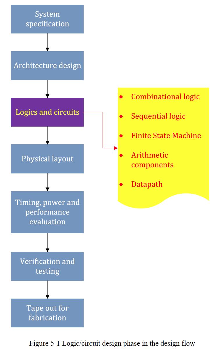
3 In the previous chapters we have studied how to develop a specification from a given application, and also discussed how to develop the architecture of the chip to be designed. Once the architecture is ready, a designer can move forward to design the logics and circuits as shown in the design flow in Figure 5 1.
4
5 As concerning modern ASIC design, most logic components, if not all, are available in a cell library, and such predesigned logic cells are optimized for both the manufacturing process and circuit performance. Only a few logic components need to be designed to fit the special needs in a real ASIC design process. In most of the cases, a logical/circuit level design can be obtained automatically by using a commercial EDA synthesis tool. The input to the synthesis tools is the RTL netlist and the output is the gate level netlist. The optimization algorithms inside the synthesis tools are very powerful and the resulting gate level netlist is in general very satisfactory.
6 The focus of this chapter is to provide basic knowledge of combinational and sequential logic circuits and to offer a reference to the commonly used logic blocks for the purpose of self-contained discussion. The material to be discussed should have already appeared in most entry-level digital circuitry courses. Readers familiar with the subject can skip over this chapter or just use it as a reference.
7 Digital logics can be divided into two main classes: combinational and sequential logics. Combinational logic usually implements a Boolean expression, where the output is purely a function of the present input. In contrast to combinational logic, the typical feature of sequential logic is its memory mechanism, which can store previous logic values, also known as states. The storage elements are commonly implemented by flip-flop or latch. Thus the output of a sequential circuit is a combined function of the present input and the state of the circuit.
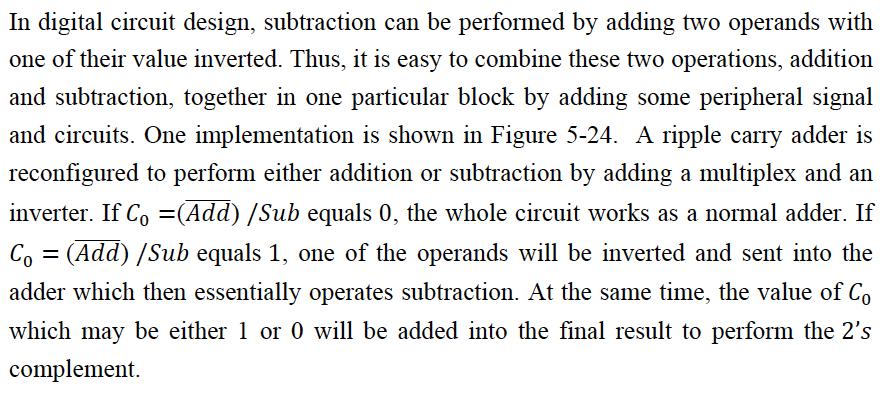
8 Combinational logic circuits are composed of gates or inverters to execute a particular function and may have one or more outputs. They play a significant role as function blocks in the digital circuit, especially, arithmetic logic circuit (ALU) where mathematical calculations are performed like addition, subtraction and multiplication. The basic combinational logic circuits include, gate, decoder, encoder and multiplexer. Some other complex combinational building blocks like adder and multiplier are used in ALU unit.
9
10
11
12 Structure of large decoder
13 Decoder is used as address selection unit in memory design

14
15

16 Application: priority encoder
17

18
19 Multiplexer circuit
20 Gate level structure
21 A 4 to 1 multiplexer
22 Computation in a digital system is carried out by arithmetic logic blocks. There are basically four arithmetic operations: addition, subtraction, multiplication and division. All of them are executed by using the fundamental gates. Their performance efficiency is critical in a digital system because they are used heavily for almost for all applications. In the following, we will discuss the basic operation principles and different topologies of two most significant arithmetic combinational blocks: Adder and Multiplier.

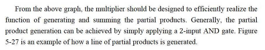
23 Circuit implementation of a full adder
24 Ripple Carry Adder
25 Circuit implementation
26 Carry look-ahead adder
27
28 Circuit structure
29 An alternative circuit structure
30 Multiplication is a complex operation in ALU which usually consumes large hardware resources and has a large propagation delay. The multiplier, in nature, is an arrangement of adder array (suppose we only use combinational circuit). Before digging into the details of the multiplier, let us look at the binary multiplication procedure. Suppose we have two four-bits binary number X and Y. A simple multiplication is performed by generating a set of partial products and summing them to get the final result. Each partial product is produced by multiplying X with each bit of Y and shifting the set of partial products with regard to the bit position of Y.
31 Figure 5 26 illustrates the multiplication procedure of two 4- bits binary numbers.
32
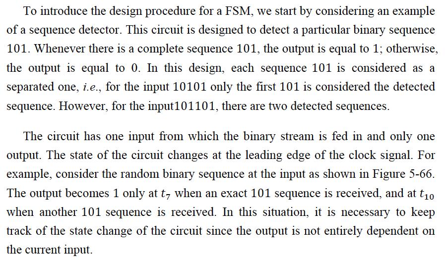
33 In this section, we will focus on another class of circuit: sequential logic circuit. Why do we need the sequential circuit? One intuitive way to answer this question is shown in Figure Suppose we have several combinational logic blocks with different functions, and the output of one block is the input of another one. Then how do we manage the data flow between the blocks, if each block needs different time to complete its computation? A solution is to employ the memory circuit to store the instant logic outputs from the combinational blocks, and latch them to the other blocks in a synchronized manner controlled by clocks.
34 Clearly, the clock period should be longer than that needed for all combinational logic blocks to complete their computation, which is usually the slowest block in the circuit. In this way, large scale digital system can be practically built.
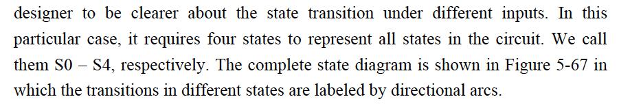
35 Latch and flip-flop are two fundamental sequential logic blocks which conduct data flow and operation synchronization. Both latch and flip-flop are based on a so-called bi-stable circuit. The bi-stable circuit is a type of circuit that has two stable states, each representing logic 0 or 1, respectively. It is widely used as the storage element in digital logic design. Figure 5 34 shows an example of such bi-stable circuit.
36 A bi-stable circuit

37 An SR Latch
38 Timing diagram
39 Gated latch A gated latch usually refers to a latch with a controlled signal. The output of a latch will follow the immediate change of the input when the control signal is active. In real practice, we want to know when the latch changes its state, and controls the transparent period for latch. For example, in some applications, we just want to set the latch to be transparent during the period when the clock is high. A clock can be used as a control signal. Only when the clock is high, will the latch work in the transparent mode during which the change at input will be sent to the output. As the clock goes low, the output will remain the previous state no matter how the input changes.
40 A gated SR Latch
41 Figure 5 40 shows the timing diagram of the gated SR latch. The output changes its state only when the enable signal is active. For all other periods, the output will maintain its previous values.

42 The main problem with using latch is that it has a transparent period when the control signal is active. During this period the output will change with the input. Consequently such a circuit is prone to noise and uncertainty of the input signals. To overcome this flaw, edge trigged flip-flop was designed.
43 As we have discussed, latch is a level-sensitive storage element. As long as latch operates on transparent period, the output will follow any immediate change of the input. In many practical implementations, we need our circuit to respond at the trigger point of clock, either at the rising edge or at the falling edge. Another important storage element, flip-flop is required in this situation.
44 One widely used flip-flop is the Master-slave D flip-flop. Figure 5 44 illustrates how the master-slave D flip-flop is realized. Two D-latches are connected in series and the clock of master latch is inverted and fed into the slave latch. During the period when the clock is high, the master latch is transparent and any change at input data will be sent and stored in the output of the master latch. The slave latch is disabled by the inverted clock signal during this time. After the clock transits from high to low, the slave latch goes into a transparent period. The previous data sampled in the output of the master latch will pass through the slave latch to the output.
45 A DFF circuit
46 DFF timing diagram
47 Circuit implementation

48 In real practical circuit design, controlling propagation delay is an important factor in guaranteeing a correct logic value. To ensure an expected stable output at a latch or a flip-flop, several timing parameters should be carefully designed.
49 Figure 5 49 shows three critical timing regions for a D flip-flop. The minimal time interval for the input data must be stable before the event of the clock so that the signal can be reliably sampled and is called the setup time. The minimal time interval for the data to be stable after the event of the clock so that the signal can be reliably sampled is called the hold time. Another important timing parameter is the clock-to-output delay or the propagation delay which is the delay from the event of clock to the change of the output.
50 Timing parameters of a D flip-flop
51 Ensure a proper timing
52 Timing design

53 Register usually refers to a group of coherent flip-flops used to store a set of n-bit wide data. It is an extremely significant block in sequential logic design since the stored data might be updated at every clock cycle and be used to keep a correct function of the whole circuit. In this section, we will mainly discuss the shift register and its application in digital logic design.
54 A basic shift register
55 SIPO The shift register can be modified into a serial in parallel out shift register (SIPO) by changing the method of accessing the output. Figure 5 52 shows a circuit implementation and operation principle for the SIPO.
56
57 PISO In contrast to the two previous shift registers, the configuration of parallel in serial out (PISO) is more complicated since the PISO circuit should be able to switch between two operation modes: parallel loading and serial shifting. Because both the serial and parallel inputs are required, another mode called switching input should also be included.
58
59 A counter is usually composed of a series of cascading flip-flops. As an indispensable element in digital logic circuitry, it serves a variety of different purposes. It can be used to either record the time pulses for a particular event or to control the timing by setting up an intentional time interval.
60 Synchronous Counter A simple circuit implementation of a synchronous counter is shown in Figure All individual flip-flops in this specific structure change their state concurrently according to an instant clock signal. Figure 5 57 gives the timing diagram of this synchronous counter.
61
62
63 With an enable control
64 Earlier in this chapter as we introduced the sequential circuit, a security system was shown to illustrate an Finite State Machine (FSM). In the flowing we discuss in detail how to design such an FSM step by step. We will also show how to use FSM in the digital system design.
65
66 Mealy State Machine Output depends on the current state and input
67 Moore State Machine Output depends only on the current state
68
69
70 State diagram
71 State transition table

72 State coding
73 Logic expression
74 Circuit implementation
75
76 FSM as the control unit for a datapath circuit
77 A digital processor usually consists of three parts: controller, ALU and interface. As is shown in Figure 5 79, the control block is the brain of the processor and it supervises and instructs each unit working cooperatively. The interface is responsible for the communication between the processor and external devices. The ALU block is the core part of the processor where most of the operations are executed, and it takes large hardware resources and the most part of the area.
78 Datapath of an FIR processor
79 In this chapter we summarized the basic combinational and sequential logics. In the discussion we have reviewed the most commonly used circuit blocks in terms of their function and structure. These circuits can be easily modified to fit most application needs. The materials discussed here usually appear in undergraduate digital circuit courses. The intent of putting them here is for the self-completion of the discussion, and as a reference.

80 1. Explain the difference between combinational and sequential logics. Give an example. 2. Show that a JK flip-flop can be constructed using a T flip-flop and other logic gates. 3. Write a VHDL code that represents an eight-bit Johnson counter. Synthesize the code with CAD tools and give a timing simulation that shows the counting sequence. 4. Determine the number of gates needed to implement an eight-bit carry-look ahead adder assuming that the maximum fan-in for the gates is four. 5. Design an ALU to be used in the implementation of the MSDAP. 6. Design a shifter register to be used as an implementation of the input functional block of the MSDAP.
Chapter 6. Flip-Flops and Simple Flip-Flop Applications
 Chapter 6 Flip-Flops and Simple Flip-Flop Applications Basic bistable element It is a circuit having two stable conditions (states). It can be used to store binary symbols. J. C. Huang, 2004 Digital Logic
Chapter 5 Synchronous Sequential Logic
 Chapter 5 Synchronous Sequential Logic Chih-Tsun Huang ( 黃稚存 ) http://nthucad.cs.nthu.edu.tw/~cthuang/ Department of Computer Science National Tsing Hua University Outline Introduction Storage Elements:
Chapter 3. Boolean Algebra and Digital Logic
 Chapter 3 Boolean Algebra and Digital Logic Chapter 3 Objectives Understand the relationship between Boolean logic and digital computer circuits. Learn how to design simple logic circuits. Understand how
Flip Flop. S-R Flip Flop. Sequential Circuits. Block diagram. Prepared by:- Anwar Bari
 Sequential Circuits The combinational circuit does not use any memory. Hence the previous state of input does not have any effect on the present state of the circuit. But sequential circuit has memory
1. Convert the decimal number to binary, octal, and hexadecimal.
 1. Convert the decimal number 435.64 to binary, octal, and hexadecimal. 2. Part A. Convert the circuit below into NAND gates. Insert or remove inverters as necessary. Part B. What is the propagation delay
DIGITAL SYSTEM FUNDAMENTALS (ECE421) DIGITAL ELECTRONICS FUNDAMENTAL (ECE422) LATCHES and FLIP-FLOPS
 DIGITAL ELECTRONICS FUNDAMENTAL (ECE422) LATCHES and FLIP-FLOPS") COURSE / CODE DIGITAL SYSTEM FUNDAMENTALS (ECE421) DIGITAL ELECTRONICS FUNDAMENTAL (ECE422) LATCHES and FLIP-FLOPS In the same way that logic gates are the building blocks of combinatorial circuits, latches
COURSE / CODE DIGITAL SYSTEM FUNDAMENTALS (ECE421) DIGITAL ELECTRONICS FUNDAMENTAL (ECE422) LATCHES and FLIP-FLOPS In the same way that logic gates are the building blocks of combinatorial circuits, latches
Microprocessor Design
 Microprocessor Design Principles and Practices With VHDL Enoch O. Hwang Brooks / Cole 2004 To my wife and children Windy, Jonathan and Michelle Contents 1. Designing a Microprocessor... 2 1.1 Overview
Combinational vs Sequential
 Combinational vs Sequential inputs X Combinational Circuits outputs Z A combinational circuit: At any time, outputs depends only on inputs Changing inputs changes outputs No regard for previous inputs
SEQUENTIAL LOGIC. Satish Chandra Assistant Professor Department of Physics P P N College, Kanpur
 SEQUENTIAL LOGIC Satish Chandra Assistant Professor Department of Physics P P N College, Kanpur www.satish0402.weebly.com OSCILLATORS Oscillators is an amplifier which derives its input from output. Oscillators
problem maximum score 1 28pts 2 10pts 3 10pts 4 15pts 5 14pts 6 12pts 7 11pts total 100pts
 University of California at Berkeley College of Engineering Department of Electrical Engineering and Computer Sciences EECS150 J. Wawrzynek Spring 2002 4/5/02 Midterm Exam II Name: Solutions ID number:
Advanced Devices. Registers Counters Multiplexers Decoders Adders. CSC258 Lecture Slides Steve Engels, 2006 Slide 1 of 20
 Advanced Devices Using a combination of gates and flip-flops, we can construct more sophisticated logical devices. These devices, while more complex, are still considered fundamental to basic logic design.
Digital Fundamentals: A Systems Approach
 Digital Fundamentals: A Systems Approach Counters Chapter 8 A System: Digital Clock Digital Clock: Counter Logic Diagram Digital Clock: Hours Counter & Decoders Finite State Machines Moore machine: One
CSE115: Digital Design Lecture 23: Latches & Flip-Flops
 Faculty of Engineering CSE115: Digital Design Lecture 23: Latches & Flip-Flops Sections 7.1-7.2 Suggested Reading A Generic Digital Processor Building Blocks for Digital Architectures INPUT - OUTPUT Interconnect:
Find the equivalent decimal value for the given value Other number system to decimal ( Sample)
") VELAMMAL COLLEGE OF ENGINEERING AND TECHNOLOGY, MADURAI 65 009 Department of Information Technology Model Exam-II-Question bank PART A (Answer for all Questions) (8 X = 6) K CO Marks Find the equivalent
VELAMMAL COLLEGE OF ENGINEERING AND TECHNOLOGY, MADURAI 65 009 Department of Information Technology Model Exam-II-Question bank PART A (Answer for all Questions) (8 X = 6) K CO Marks Find the equivalent
Read-only memory (ROM) Digital logic: ALUs Sequential logic circuits. Don't cares. Bus
 Digital logic: ALUs Sequential logic circuits. Don't cares. Bus") Digital logic: ALUs Sequential logic circuits CS207, Fall 2004 October 11, 13, and 15, 2004 1 Read-only memory (ROM) A form of memory Contents fixed when circuit is created n input lines for 2 n addressable
Digital logic: ALUs Sequential logic circuits CS207, Fall 2004 October 11, 13, and 15, 2004 1 Read-only memory (ROM) A form of memory Contents fixed when circuit is created n input lines for 2 n addressable
COE328 Course Outline. Fall 2007
 COE28 Course Outline Fall 2007 1 Objectives This course covers the basics of digital logic circuits and design. Through the basic understanding of Boolean algebra and number systems it introduces the student
NH 67, Karur Trichy Highways, Puliyur C.F, Karur District UNIT-III SEQUENTIAL CIRCUITS
 NH 67, Karur Trichy Highways, Puliyur C.F, 639 114 Karur District DEPARTMENT OF ELETRONICS AND COMMUNICATION ENGINEERING COURSE NOTES SUBJECT: DIGITAL ELECTRONICS CLASS: II YEAR ECE SUBJECT CODE: EC2203
Counters
 Counters A counter is the most versatile and useful subsystems in the digital system. A counter driven by a clock can be used to count the number of clock cycles. Since clock pulses occur at known intervals,
Contents Circuits... 1
 Contents Circuits... 1 Categories of Circuits... 1 Description of the operations of circuits... 2 Classification of Combinational Logic... 2 1. Adder... 3 2. Decoder:... 3 Memory Address Decoder... 5 Encoder...
CHAPTER 4: Logic Circuits
 CHAPTER 4: Logic Circuits II. Sequential Circuits Combinational circuits o The outputs depend only on the current input values o It uses only logic gates, decoders, multiplexers, ALUs Sequential circuits
Vignana Bharathi Institute of Technology UNIT 4 DLD
 DLD UNIT IV Synchronous Sequential Circuits, Latches, Flip-flops, analysis of clocked sequential circuits, Registers, Shift registers, Ripple counters, Synchronous counters, other counters. Asynchronous
Introduction to Digital Logic Missouri S&T University CPE 2210 Exam 3 Logistics
 Introduction to Digital Logic Missouri S&T University CPE 2210 Exam 3 Logistics Egemen K. Çetinkaya Egemen K. Çetinkaya Department of Electrical & Computer Engineering Missouri University of Science and
Solution to Digital Logic )What is the magnitude comparator? Design a logic circuit for 4 bit magnitude comparator and explain it,
What is the magnitude comparator? Design a logic circuit for 4 bit magnitude comparator and explain it,") Solution to Digital Logic -2067 Solution to digital logic 2067 1.)What is the magnitude comparator? Design a logic circuit for 4 bit magnitude comparator and explain it, A Magnitude comparator is a combinational
Solution to Digital Logic -2067 Solution to digital logic 2067 1.)What is the magnitude comparator? Design a logic circuit for 4 bit magnitude comparator and explain it, A Magnitude comparator is a combinational
CHAPTER 4: Logic Circuits
 CHAPTER 4: Logic Circuits II. Sequential Circuits Combinational circuits o The outputs depend only on the current input values o It uses only logic gates, decoders, multiplexers, ALUs Sequential circuits
Chapter 5: Synchronous Sequential Logic
 Chapter 5: Synchronous Sequential Logic NCNU_2016_DD_5_1 Digital systems may contain memory for storing information. Combinational circuits contains no memory elements the outputs depends only on the inputs
Logic Design II (17.342) Spring Lecture Outline
 Spring Lecture Outline") Logic Design II (17.342) Spring 2012 Lecture Outline Class # 03 February 09, 2012 Dohn Bowden 1 Today s Lecture Registers and Counters Chapter 12 2 Course Admin 3 Administrative Admin for tonight Syllabus
Logic Design II (17.342) Spring 2012 Lecture Outline Class # 03 February 09, 2012 Dohn Bowden 1 Today s Lecture Registers and Counters Chapter 12 2 Course Admin 3 Administrative Admin for tonight Syllabus
Chapter 4. Logic Design
 Chapter 4 Logic Design 4.1 Introduction. In previous Chapter we studied gates and combinational circuits, which made by gates (AND, OR, NOT etc.). That can be represented by circuit diagram, truth table
IT T35 Digital system desigm y - ii /s - iii
 UNIT - III Sequential Logic I Sequential circuits: latches flip flops analysis of clocked sequential circuits state reduction and assignments Registers and Counters: Registers shift registers ripple counters
MODULE 3. Combinational & Sequential logic
 MODULE 3 Combinational & Sequential logic Combinational Logic Introduction Logic circuit may be classified into two categories. Combinational logic circuits 2. Sequential logic circuits A combinational
Flip-Flops. Because of this the state of the latch may keep changing in circuits with feedback as long as the clock pulse remains active.
 Flip-Flops Objectives The objectives of this lesson are to study: 1. Latches versus Flip-Flops 2. Master-Slave Flip-Flops 3. Timing Analysis of Master-Slave Flip-Flops 4. Different Types of Master-Slave
Lecture 8: Sequential Logic
 Lecture 8: Sequential Logic Last lecture discussed how we can use digital electronics to do combinatorial logic we designed circuits that gave an immediate output when presented with a given set of inputs
WINTER 15 EXAMINATION Model Answer
 Important Instructions to examiners: 1) The answers should be examined by key words and not as word-to-word as given in the model answer scheme. 2) The model answer and the answer written by candidate
Multiplexor (aka MUX) An example, yet VERY useful circuit!
 An example, yet VERY useful circuit!") Multiplexor (aka MUX) An example, yet VERY useful circuit! A B 0 1 Y S A B Y 0 0 x 0 0 1 x 1 1 x 0 0 1 x 1 1 S=1 S=0 Y = (S)? B:A; Y=S A+SB when S = 0: output A 1: output B 56 A 32-bit MUX Use 32 1-bit
Multiplexor (aka MUX) An example, yet VERY useful circuit! A B 0 1 Y S A B Y 0 0 x 0 0 1 x 1 1 x 0 0 1 x 1 1 S=1 S=0 Y = (S)? B:A; Y=S A+SB when S = 0: output A 1: output B 56 A 32-bit MUX Use 32 1-bit
Logic Design Viva Question Bank Compiled By Channveer Patil
 Logic Design Viva Question Bank Compiled By Channveer Patil Title of the Practical: Verify the truth table of logic gates AND, OR, NOT, NAND and NOR gates/ Design Basic Gates Using NAND/NOR gates. Q.1
Module -5 Sequential Logic Design
 Module -5 Sequential Logic Design 5.1. Motivation: In digital circuit theory, sequential logic is a type of logic circuit whose output depends not only on the present value of its input signals but on
Counter dan Register
 Counter dan Register Introduction Circuits for counting events are frequently used in computers and other digital systems. Since a counter circuit must remember its past states, it has to possess memory.
Sequential Logic. Analysis and Synthesis. Joseph Cavahagh Santa Clara University. r & Francis. TaylonSi Francis Group. , Boca.Raton London New York \
 Sequential Logic Analysis and Synthesis Joseph Cavahagh Santa Clara University r & Francis TaylonSi Francis Group, Boca.Raton London New York \ CRC is an imprint of the Taylor & Francis Group, an informa
Sequencing. Lan-Da Van ( 范倫達 ), Ph. D. Department of Computer Science National Chiao Tung University Taiwan, R.O.C. Fall,
, Ph. D. Department of Computer Science National Chiao Tung University Taiwan, R.O.C. Fall,") Sequencing ( 范倫達 ), Ph. D. Department of Computer Science National Chiao Tung University Taiwan, R.O.C. Fall, 2013 ldvan@cs.nctu.edu.tw http://www.cs.nctu.edu.tw/~ldvan/ Outlines Introduction Sequencing
Sequencing ( 范倫達 ), Ph. D. Department of Computer Science National Chiao Tung University Taiwan, R.O.C. Fall, 2013 ldvan@cs.nctu.edu.tw http://www.cs.nctu.edu.tw/~ldvan/ Outlines Introduction Sequencing
Unit-5 Sequential Circuits - 1
 Unit-5 Sequential Circuits - 1 1. With the help of block diagram, explain the working of a JK Master-Slave flip flop. 2. Differentiate between combinational circuit and sequential circuit. 3. Explain Schmitt
Combinational / Sequential Logic
 Digital Circuit Design and Language Combinational / Sequential Logic Chang, Ik Joon Kyunghee University Combinational Logic + The outputs are determined by the present inputs + Consist of input/output
Logic Design. Flip Flops, Registers and Counters
 Logic Design Flip Flops, Registers and Counters Introduction Combinational circuits: value of each output depends only on the values of inputs Sequential Circuits: values of outputs depend on inputs and
Logic and Computer Design Fundamentals. Chapter 7. Registers and Counters
 Logic and Computer Design Fundamentals Chapter 7 Registers and Counters Registers Register a collection of binary storage elements In theory, a register is sequential logic which can be defined by a state
Experiment 8 Introduction to Latches and Flip-Flops and registers
 Experiment 8 Introduction to Latches and Flip-Flops and registers Introduction: The logic circuits that have been used until now were combinational logic circuits since the output of the device depends
UNIT-3: SEQUENTIAL LOGIC CIRCUITS
 UNIT-3: SEQUENTIAL LOGIC CIRCUITS STRUCTURE 3. Objectives 3. Introduction 3.2 Sequential Logic Circuits 3.2. NAND Latch 3.2.2 RS Flip-Flop 3.2.3 D Flip-Flop 3.2.4 JK Flip-Flop 3.2.5 Edge Triggered RS Flip-Flop
Dr. Shahram Shirani COE2DI4 Midterm Test #2 Nov 19, 2008
 Page 1 Dr. Shahram Shirani COE2DI4 Midterm Test #2 Nov 19, 2008 Instructions: This examination paper includes 13 pages and 20 multiple-choice questions starting on page 3. You are responsible for ensuring
D Latch (Transparent Latch)
") D Latch (Transparent Latch) -One way to eliminate the undesirable condition of the indeterminate state in the SR latch is to ensure that inputs S and R are never equal to 1 at the same time. This is done
D Latch (Transparent Latch) -One way to eliminate the undesirable condition of the indeterminate state in the SR latch is to ensure that inputs S and R are never equal to 1 at the same time. This is done
Previous Lecture Sequential Circuits. Slide Summary of contents covered in this lecture. (Refer Slide Time: 01:55)
") Previous Lecture Sequential Circuits Digital VLSI System Design Prof. S. Srinivasan Department of Electrical Engineering Indian Institute of Technology, Madras Lecture No 7 Sequential Circuit Design Slide
Previous Lecture Sequential Circuits Digital VLSI System Design Prof. S. Srinivasan Department of Electrical Engineering Indian Institute of Technology, Madras Lecture No 7 Sequential Circuit Design Slide
VeriLab. An introductory lab for using Verilog in digital design (first draft) VeriLab
 VeriLab") VeriLab An introductory lab for using Verilog in digital design (first draft) VeriLab An introductory lab for using Verilog in digital design Verilog is a hardware description language useful for designing
VeriLab An introductory lab for using Verilog in digital design (first draft) VeriLab An introductory lab for using Verilog in digital design Verilog is a hardware description language useful for designing
We are here. Assembly Language. Processors Arithmetic Logic Units. Finite State Machines. Circuits Gates. Transistors
 CSC258 Week 5 1 We are here Assembly Language Processors Arithmetic Logic Units Devices Finite State Machines Flip-flops Circuits Gates Transistors 2 Circuits using flip-flops Now that we know about flip-flops
Final Exam review: chapter 4 and 5. Supplement 3 and 4
 Final Exam review: chapter 4 and 5. Supplement 3 and 4 1. A new type of synchronous flip-flop has the following characteristic table. Find the corresponding excitation table with don t cares used as much
MODEL QUESTIONS WITH ANSWERS THIRD SEMESTER B.TECH DEGREE EXAMINATION DECEMBER CS 203: Switching Theory and Logic Design. Time: 3 Hrs Marks: 100
 MODEL QUESTIONS WITH ANSWERS THIRD SEMESTER B.TECH DEGREE EXAMINATION DECEMBER 2016 CS 203: Switching Theory and Logic Design Time: 3 Hrs Marks: 100 PART A ( Answer All Questions Each carries 3 Marks )
Digital Design, Kyung Hee Univ. Chapter 5. Synchronous Sequential Logic
 Chapter 5. Synchronous Sequential Logic 1 5.1 Introduction Electronic products: ability to send, receive, store, retrieve, and process information in binary format Dependence on past values of inputs Sequential
Synchronous Sequential Logic. Chapter 5
 Synchronous Sequential Logic Chapter 5 5-1 Introduction Combinational circuits contains no memory elements the outputs depends on the inputs Synchronous Sequential Logic 5-2 5-2 Sequential Circuits Sequential
COMP2611: Computer Organization. Introduction to Digital Logic
 1 COMP2611: Computer Organization Sequential Logic Time 2 Till now, we have essentially ignored the issue of time. We assume digital circuits: Perform their computations instantaneously Stateless: once
CHAPTER 6 COUNTERS & REGISTERS
 CHAPTER 6 COUNTERS & REGISTERS 6.1 Asynchronous Counter 6.2 Synchronous Counter 6.3 State Machine 6.4 Basic Shift Register 6.5 Serial In/Serial Out Shift Register 6.6 Serial In/Parallel Out Shift Register
1. a) For the circuit shown in figure 1.1, draw a truth table showing the output Q for all combinations of inputs A, B and C. [4] Figure 1.
![1. a) For the circuit shown in figure 1.1, draw a truth table showing the output Q for all combinations of inputs A, B and C. [4] Figure 1.](/thumbs/88/117492374.jpg "1. a) For the circuit shown in figure 1.1, draw a truth table showing the output Q for all combinations of inputs A, B and C. [4] Figure 1.") [Question 1 is compulsory] 1. a) For the circuit shown in figure 1.1, draw a truth table showing the output Q for all combinations of inputs A, B and C. Figure 1.1 b) Minimize the following Boolean functions:
[Question 1 is compulsory] 1. a) For the circuit shown in figure 1.1, draw a truth table showing the output Q for all combinations of inputs A, B and C. Figure 1.1 b) Minimize the following Boolean functions:
COE 202: Digital Logic Design Sequential Circuits Part 1. Dr. Ahmad Almulhem ahmadsm AT kfupm Phone: Office:
 COE 202: Digital Logic Design Sequential Circuits Part 1 Dr. Ahmad Almulhem Email: ahmadsm AT kfupm Phone: 860-7554 Office: 22-324 Objectives Sequential Circuits Memory Elements Latches Flip-Flops Combinational
A clock is a free-running signal with a cycle time. A clock may be either high or low, and alternates between the two states.
 Clocks A clock is a free-running signal with a cycle time. A clock may be either high or low, and alternates between the two states. 1 The length of time the clock is high before changing states is its
 UNIT 1 NUMBER SYSTEMS AND DIGITAL LOGIC FAMILIES 1. Briefly explain the stream lined method of converting binary to decimal number with example. 2. Give the Gray code for the binary number (111) 2. 3.
Chapter. Synchronous Sequential Circuits
 Chapter 5 Synchronous Sequential Circuits Logic Circuits- Review Logic Circuits 2 Combinational Circuits Consists of logic gates whose outputs are determined from the current combination of inputs. Performs
DIGITAL SYSTEM DESIGN UNIT I (2 MARKS)
") DIGITAL SYSTEM DESIGN UNIT I (2 MARKS) 1. Convert Binary number (111101100) 2 to Octal equivalent. 2. Convert Binary (1101100010011011) 2 to Hexadecimal equivalent. 3. Simplify the following Boolean function
DIGITAL SYSTEM DESIGN UNIT I (2 MARKS) 1. Convert Binary number (111101100) 2 to Octal equivalent. 2. Convert Binary (1101100010011011) 2 to Hexadecimal equivalent. 3. Simplify the following Boolean function
CS8803: Advanced Digital Design for Embedded Hardware
 CS883: Advanced Digital Design for Embedded Hardware Lecture 4: Latches, Flip-Flops, and Sequential Circuits Instructor: Sung Kyu Lim (limsk@ece.gatech.edu) Website: http://users.ece.gatech.edu/limsk/course/cs883
Electrical and Telecommunications Engineering Technology_TCET3122/TC520. NEW YORK CITY COLLEGE OF TECHNOLOGY The City University of New York
 NEW YORK CITY COLLEGE OF TECHNOLOGY The City University of New York DEPARTMENT: SUBJECT CODE AND TITLE: COURSE DESCRIPTION: REQUIRED: Electrical and Telecommunications Engineering Technology TCET 3122/TC
Digital Logic Design Sequential Circuits. Dr. Basem ElHalawany
 Digital Logic Design Sequential Circuits Dr. Basem ElHalawany Combinational vs Sequential inputs X Combinational Circuits outputs Z A combinational circuit: At any time, outputs depends only on inputs
More on Flip-Flops Digital Design and Computer Architecture: ARM Edition 2015 Chapter 3 <98> 98
 More on Flip-Flops Digital Design and Computer Architecture: ARM Edition 2015 Chapter 3 98 Review: Bit Storage SR latch S (set) Q R (reset) Level-sensitive SR latch S S1 C R R1 Q D C S R D latch Q
AIM: To study and verify the truth table of logic gates
 EXPERIMENT: 1- LOGIC GATES AIM: To study and verify the truth table of logic gates LEARNING OBJECTIVE: Identify various Logic gates and their output. COMPONENTS REQUIRED: KL-31001 Digital Logic Lab( Main
Name Of The Experiment: Sequential circuit design Latch, Flip-flop and Registers
 EEE 304 Experiment No. 07 Name Of The Experiment: Sequential circuit design Latch, Flip-flop and Registers Important: Submit your Prelab at the beginning of the lab. Prelab 1: Construct a S-R Latch and
Memory elements. Topics. Memory element terminology. Variations in memory elements. Clock terminology. Memory element parameters. clock.
 Topics! Memory elements.! Basics of sequential machines. Memory elements! Stores a value as controlled by clock.! May have load signal, etc.! In CMOS, memory is created by:! capacitance (dynamic);! feedback
Logic Design ( Part 3) Sequential Logic- Finite State Machines (Chapter 3)
 Sequential Logic- Finite State Machines (Chapter 3)") Logic esign ( Part ) Sequential Logic- Finite State Machines (Chapter ) Based on slides McGraw-Hill Additional material 00/00/006 Lewis/Martin Additional material 008 Roth Additional material 00 Taylor
Logic esign ( Part ) Sequential Logic- Finite State Machines (Chapter ) Based on slides McGraw-Hill Additional material 00/00/006 Lewis/Martin Additional material 008 Roth Additional material 00 Taylor
Principles of Computer Architecture. Appendix A: Digital Logic
 A-1 Appendix A - Digital Logic Principles of Computer Architecture Miles Murdocca and Vincent Heuring Appendix A: Digital Logic A-2 Appendix A - Digital Logic Chapter Contents A.1 Introduction A.2 Combinational
BCN1043. By Dr. Mritha Ramalingam. Faculty of Computer Systems & Software Engineering
 BCN1043 By Dr. Mritha Ramalingam Faculty of Computer Systems & Software Engineering mritha@ump.edu.my http://ocw.ump.edu.my/ authors Dr. Mohd Nizam Mohmad Kahar (mnizam@ump.edu.my) Jamaludin Sallim (jamal@ump.edu.my)
Low Power VLSI Circuits and Systems Prof. Ajit Pal Department of Computer Science and Engineering Indian Institute of Technology, Kharagpur
 Low Power VLSI Circuits and Systems Prof. Ajit Pal Department of Computer Science and Engineering Indian Institute of Technology, Kharagpur Lecture No. # 29 Minimizing Switched Capacitance-III. (Refer
Asynchronous (Ripple) Counters
 Counters") Circuits for counting events are frequently used in computers and other digital systems. Since a counter circuit must remember its past states, it has to possess memory. The chapter about flip-flops introduced
Circuits for counting events are frequently used in computers and other digital systems. Since a counter circuit must remember its past states, it has to possess memory. The chapter about flip-flops introduced
Chapter Contents. Appendix A: Digital Logic. Some Definitions
 A- Appendix A - Digital Logic A-2 Appendix A - Digital Logic Chapter Contents Principles of Computer Architecture Miles Murdocca and Vincent Heuring Appendix A: Digital Logic A. Introduction A.2 Combinational
Part 4: Introduction to Sequential Logic. Basic Sequential structure. Positive-edge-triggered D flip-flop. Flip-flops classified by inputs
 Part 4: Introduction to Sequential Logic Basic Sequential structure There are two kinds of components in a sequential circuit: () combinational blocks (2) storage elements Combinational blocks provide
Registers and Counters
 Registers and Counters Clocked sequential circuit = F/Fs and combinational gates Register Group of flip-flops (share a common clock and capable of storing one bit of information) Consist of a group of
Introduction to Digital Logic Missouri S&T University CPE 2210 Exam 2 Logistics
 Introduction to Digital Logic Missouri S&T University CPE 2210 Exam 2 Logistics Egemen K. Çetinkaya Egemen K. Çetinkaya Department of Electrical & Computer Engineering Missouri University of Science and
Introduction. NAND Gate Latch. Digital Logic Design 1 FLIP-FLOP. Digital Logic Design 1
 2007 Introduction BK TP.HCM FLIP-FLOP So far we have seen Combinational Logic The output(s) depends only on the current values of the input variables Here we will look at Sequential Logic circuits The
Logic Devices for Interfacing, The 8085 MPU Lecture 4
 Logic Devices for Interfacing, The 8085 MPU Lecture 4 1 Logic Devices for Interfacing Tri-State devices Buffer Bidirectional Buffer Decoder Encoder D Flip Flop :Latch and Clocked 2 Tri-state Logic Outputs
Unit 11. Latches and Flip-Flops
 Unit 11 Latches and Flip-Flops 1 Combinational Circuits A combinational circuit consists of logic gates whose outputs, at any time, are determined by combining the values of the inputs. For n input variables,
COMP12111: Fundamentals of Computer Engineering
 COMP2: Fundamentals of Computer Engineering Part I Course Overview & Introduction to Logic Paul Nutter Introduction What is this course about? Computer hardware design o not electronics nothing nasty like
Switching Theory And Logic Design UNIT-IV SEQUENTIAL LOGIC CIRCUITS
 Switching Theory And Logic Design UNIT-IV SEQUENTIAL LOGIC CIRCUITS Sequential circuits Classification of sequential circuits: Sequential circuits may be classified as two types. 1. Synchronous sequential
COMP sequential logic 1 Jan. 25, 2016
 OMP 273 5 - sequential logic 1 Jan. 25, 2016 Sequential ircuits All of the circuits that I have discussed up to now are combinational digital circuits. For these circuits, each output is a logical combination
Introduction to Sequential Circuits
 Introduction to Sequential Circuits COE 202 Digital Logic Design Dr. Muhamed Mudawar King Fahd University of Petroleum and Minerals Presentation Outline Introduction to Sequential Circuits Synchronous
QUICK GUIDE COMPUTER LOGICAL ORGANIZATION - OVERVIEW
 QUICK GUIDE http://www.tutorialspoint.com/computer_logical_organization/computer_logical_organization_quick_guide.htm COMPUTER LOGICAL ORGANIZATION - OVERVIEW Copyright tutorialspoint.com In the modern
EEC 118 Lecture #9: Sequential Logic. Rajeevan Amirtharajah University of California, Davis Jeff Parkhurst Intel Corporation
 EEC 118 Lecture #9: Sequential Logic Rajeevan Amirtharajah University of California, Davis Jeff Parkhurst Intel Corporation Outline Review: Static CMOS Logic Finish Static CMOS transient analysis Sequential
CS6201 UNIT I PART-A. Develop or build the following Boolean function with NAND gate F(x,y,z)=(1,2,3,5,7).
=(1,2,3,5,7).") VALLIAMMAI ENGINEERING COLLEGE SRM Nagar, Kattankulathur-603203 DEPARTMENT OF COMPUTER SCIENCE AND ENGINEERING Academic Year: 2015-16 BANK - EVEN SEMESTER UNIT I PART-A 1 Find the octal equivalent of hexadecimal
VALLIAMMAI ENGINEERING COLLEGE SRM Nagar, Kattankulathur-603203 DEPARTMENT OF COMPUTER SCIENCE AND ENGINEERING Academic Year: 2015-16 BANK - EVEN SEMESTER UNIT I PART-A 1 Find the octal equivalent of hexadecimal
Serial In/Serial Left/Serial Out Operation
 Shift Registers The need to storage binary data was discussed earlier. In digital circuits multi-bit data has to be stored temporarily until it is processed. A flip-flop is able to store a single binary
CS T34-DIGITAL SYSTEM DESIGN Y2/S3
 UNIT III Sequential Logic: Latches versus Flip Flops SR, D, JK, Master Slave Flip Flops Excitation table Conversion of Flip flops Counters: Asynchronous, synchronous, decade, presettable Shift Registers:
Chapter 2. Digital Circuits
 Chapter 2. Digital Circuits Logic gates Flip-flops FF registers IC registers Data bus Encoders/Decoders Multiplexers Troubleshooting digital circuits Most contents of this chapter were covered in 88-217
MAHARASHTRA STATE BOARD OF TECHNICAL EDUCATION (Autonomous) (ISO/IEC Certified)
 (ISO/IEC Certified)") Important Instructions to examiners: 1) The answers should be examined by key words and not as word-to-word as given in the model answer scheme. 2) The model answer and the answer written by candidate
Important Instructions to examiners: 1) The answers should be examined by key words and not as word-to-word as given in the model answer scheme. 2) The model answer and the answer written by candidate
UNIVERSITI TEKNOLOGI MALAYSIA
 SULIT Faculty of Computing UNIVERSITI TEKNOLOGI MALAYSIA FINAL EXAMINATION SEMESTER I, 2016 / 2017 SUBJECT CODE : SUBJECT NAME : SECTION : TIME : DATE/DAY : VENUES : INSTRUCTIONS : Answer all questions
Chapter 7 Counters and Registers
 Chapter 7 Counters and Registers Chapter 7 Objectives Selected areas covered in this chapter: Operation & characteristics of synchronous and asynchronous counters. Analyzing and evaluating various types
ECE 263 Digital Systems, Fall 2015
 ECE 263 Digital Systems, Fall 2015 REVIEW: FINALS MEMORY ROM, PROM, EPROM, EEPROM, FLASH RAM, DRAM, SRAM Design of a memory cell 1. Draw circuits and write 2 differences and 2 similarities between DRAM
ELCT201: DIGITAL LOGIC DESIGN
 ELCT201: DIGITAL LOGIC DESIGN Dr. Eng. Haitham Omran, haitham.omran@guc.edu.eg Dr. Eng. Wassim Alexan, wassim.joseph@guc.edu.eg Lecture 6 Following the slides of Dr. Ahmed H. Madian ذو الحجة 1438 ه Winter
R13 SET - 1 '' ''' '' ' '''' Code No: RT21053
 SET - 1 1. a) What are the characteristics of 2 s complement numbers? b) State the purpose of reducing the switching functions to minimal form. c) Define half adder. d) What are the basic operations in
Chapter 11 Latches and Flip-Flops
 Chapter 11 Latches and Flip-Flops SKEE1223 igital Electronics Mun im/arif/izam FKE, Universiti Teknologi Malaysia ecember 8, 2015 Types of Logic Circuits Combinational logic: Output depends solely on the
Sequential circuits. Same input can produce different output. Logic circuit. William Sandqvist
 Sequential circuits Same input can produce different output Logic circuit If the same input may produce different output signal, we have a sequential logic circuit. It must then have an internal memory
 WWW.STUDENTSFOCUS.COM + Class Subject Code Subject Prepared By Lesson Plan for Time: Lesson. No 1.CONTENT LIST: Introduction to Unit III 2. SKILLS ADDRESSED: Listening I year, 02 sem CS6201 Digital Principles
LESSON PLAN. Sub Code: EE2255 Sub Name: DIGITAL LOGIC CIRCUITS Unit: I Branch: EEE Semester: IV
 Unit: I Branch: EEE Semester: IV Page 1 of 6 Unit I Syllabus: BOOLEAN ALGEBRA AND COMBINATIONAL CIRCUITS 9 Boolean algebra: De-Morgan s theorem, switching functions and simplification using K-maps & Quine