Wafer Thinning and Thru-Silicon Vias
|
|
|
- Sydney Bridges
- 6 years ago
- Views:
Transcription


1 Wafer Thinning and Thru-Silicon Vias The Path to Wafer Level Packaging
2 Summary A new dry etching technology Atmospheric Downstream Plasma (ADP) Etch Applications to Packaging Wafer Thinning Cavity Etch 3-D Packaging Vias through Silicon Wafers All Silicon Die Packages Wafer Level Packaging
3 Wafer Thinning Requirements Wafer fab processing thickness 200mm diameter = 725 µm 300mm diameter = 810 µm Wafer thickness for packaging Year 2000 = µm Year 2002 = µm Max Die Size Year 2000 = 20 x 20mm Year 2002 = 40 x 40mm

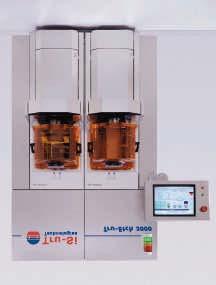
4 ADP System
5 ADP Simplifies Wafer Thinning No Device Protection Needed No Resist or Tape Application and removal No Defect Removal by Wet Etch 2-5 micron etch No Chemical Difficulties Handling Disposal Lower Chemical Cost
6 Schematic Plasma Source

7 Plasma Source
8 No-Touch Wafer Holding No contact between wafer and holder Wafer Temperature adjustable between 160 and 300 ºC Allows wafers bumped with eutectic Sn/Pb to be thinned without protective coating Thin flexible wafers held flat during processing

9 Grinding Marks Removal
10 Silicon Crystal Orientations

11 Silicon Surface Etched by ADP

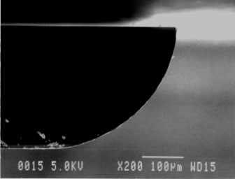
12 Wafer Edge ADP Smoothing

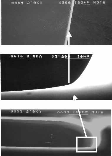
13 Before ADP After ADP
 Grind back of wafer ADP etch on back of the wafer to singulate")
14 Damage Free Dicing Controlled Depth Dicing Apply tape on front side (over dicing) Grind back of wafer ADP etch on back of the wafer to singulate dies


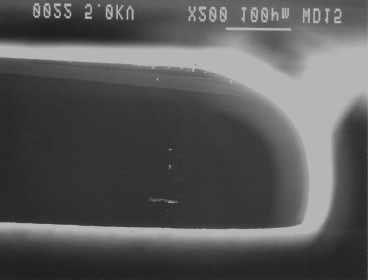
15 SEM Damage Free Dicing Sawed die shows edge chipping ADP singulated die has rounded and smooth edges
16 Damage Free Dicing Benefits: Rounded edges and corners Mechanical Strength High Reliability during Temperature shock and cycling Ultra-thin die capability 20µm dies demonstrated Smooth edge helps pick-and-place
17 Stacked Dies in <1mm packages Ultra-thin packages strictly Japanese phenomena in the early 90s New US adoption of: Smart cards Memory cards Stacked dies desirable: Reduce loop height Minimize footprint


18 Stacked Wire Bonded Dies
19 Why 3-D Packages and Wafer Stacking? Electrical performance: Reduced interconnection length. Short connections is the most effective method to improve system speed. Gang processing: Lower labor cost Familiar wafer fab equipment Improved reliability:

20 The number of transistors double every 2nd year
21 Die area doubles every 5.5 years Lineal side dimension doubles every 11 years
22 System Bandwidth Limits Performance Chip Clock rates: Much faster than board level Determined by semiconductor architecture Interconnect length << wavelength Bus clock rates: High Speed outside chip requires transmission lines Parallel operation necessary 100 MHz bus clock --> 763 MBs on 32 bit bus

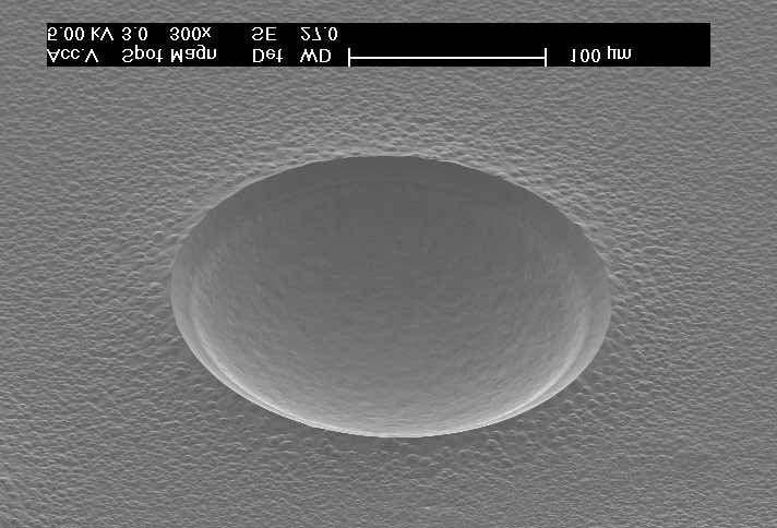
23 Array of vias (backside of wafer)

24 Test Substrate Layout - GDSII plot

25 Thru-Si Test Substrate
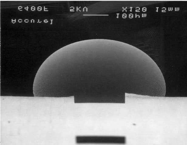
26 Interconnect Bump

27 What makes through Silicon vias tick?

28 Via Etch Masking

29 ADP Via Etch

30 ADP Via Etch (continued)

31 ADP Back Etch of via

32 Stackable Via
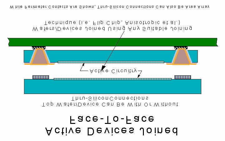
33 Tru-CSP face-to-face ICs

34 Stacked Chips: Tru-CSP

35 3-D Wafer Level Packaging

36 ADP Etch Aluminum Mask

37 Early Stage of ADP Via Etch
38 Via Hemispherical Shape

39 Wet Etched Via
40 Work in Progress Anisotropic Etching Model to predict shape of cavities Reliability Thermal Through the Silicon vias Thin Silicon Electrical Performance RLC characterization Model for CAD insertion
41 Summary of 3-D Development Short term goals: Bumped wafers All Silicon package Tiled wafers Wafer level packaging Long Term goals: 3-D Wafer Level Packaging Stacked dies Wafer level
Advancements in Acoustic Micro-Imaging Tuesday October 11th, 2016
 Central Texas Electronics Association Advancements in Acoustic Micro-Imaging Tuesday October 11th, 2016 A review of the latest advancements in Acoustic Micro-Imaging for the non-destructive inspection
Flexible Electronics Production Deployment on FPD Standards: Plastic Displays & Integrated Circuits. Stanislav Loboda R&D engineer
 Flexible Electronics Production Deployment on FPD Standards: Plastic Displays & Integrated Circuits Stanislav Loboda R&D engineer The world-first small-volume contract manufacturing for plastic TFT-arrays
Advanced WLP Platform for High-Performance MEMS. Presented by Dean Spicer, Director of Engineering
 Advanced WLP Platform for High-Performance MEMS Presented by Dean Spicer, Director of Engineering 1 May 11 th, 2016 1 Outline 1. Application Drivers for High Performance MEMS Sensors 2. Approaches to Achieving
Verification of HBM through Direct Probing on MicroBumps
 Verification of HBM through Direct Probing on MicroBumps FormFactor Sung Wook Moon SK hynix Outline HBM market HBM test flow Device structure overview Key test challenges addressed Signal delivery and
CMD GHz Fundamental Mixer
 Features Low conversion loss High isolation Wide IF bandwidth Passive double balanced topology Small die size Functional Block Diagram LO RF 1 2 Description The CMD177 is a general purpose double balanced
Parameter Min Typ Max Units Frequency Range, RF
 Features Low conversion loss High isolation Ultra wide IF bandwidth Passive double balanced topology Small die size Description The is a general purpose double balanced mixer die with ultra wide IF bandwidth
Parts of dicing machines for scribing or scoring semiconductor wafers , , , , ,
 US-Rev3 26 March 1997 With respect to any product described in or for Attachment B to the Annex to the Ministerial Declaration on Trade in Information Technology Products (WT/MIN(96)/16), to the extent
Monolithic Optoelectronic Integration of High- Voltage Power FETs and LEDs
 Monolithic Optoelectronic Integration of High- Voltage Power FETs and LEDs, Zhongda Li, Robert Karlicek and T. Paul Chow Smart Lighting Engineering Research Center Rensselaer Polytechnic Institute, Troy,
Leveraging 300 mm Technology Solutions to Enable New MEMS Process Capabilities
 Leveraging 300 mm Technology Solutions to Enable New MEMS Process Capabilities Evan Patton Semicon Europa November 2017 Lam Research Corp. 1 Presentation Outline The Internet of Things (IoT) as a market
High ResolutionCross Strip Anodes for Photon Counting detectors
 High ResolutionCross Strip Anodes for Photon Counting detectors Oswald H.W. Siegmund, Anton S. Tremsin, Robert Abiad, J. Hull and John V. Vallerga Space Sciences Laboratory University of California Berkeley,
SINGULATION BY PLASMA ETCHING. INTEGRATION TECHNIQUES TO ENABLE LOW DAMAGE, HIGH PRODUCTIVITY DICING.
 SINGULATION BY PLASMA ETCHING. INTEGRATION TECHNIQUES TO ENABLE LOW DAMAGE, HIGH PRODUCTIVITY DICING. Richard Barnett Dave Thomas Oliver Ansell ABSTRACT Plasma dicing has rapidly gained traction as a viable
SEMICONDUCTOR TECHNOLOGY -CMOS-
 SEMICONDUCTOR TECHNOLOGY -CMOS- Fire Tom Wada 2011/12/19 1 What is semiconductor and LSIs Huge number of transistors can be integrated in a small Si chip. The size of the chip is roughly the size of nails.
MAAP DIEEV1. Ka-Band 4 W Power Amplifier GHz Rev. V1. Features. Functional Diagram. Description. Pin Configuration 2
 Features Frequency Range: 32 to Small Signal Gain: 18 db Saturated Power: 37 dbm Power Added Efficiency: 23% % On-Wafer RF and DC Testing % Visual Inspection to MIL-STD-883 Method Bias V D = 6 V, I D =
Through Silicon Via Testing Known Good Die (KGD) or Probably Good Die (PGD) Doug Lefever Advantest
 or Probably Good Die (PGD) Doug Lefever Advantest") Through Silicon Via Testing Known Good Die (KGD) or Probably Good Die (PGD) Doug Lefever Advantest Single Die Fab Yield will drive Cost Equation. Yield of the device to be stacked 100% 90% 80% Yield of
Through Silicon Via Testing Known Good Die (KGD) or Probably Good Die (PGD) Doug Lefever Advantest Single Die Fab Yield will drive Cost Equation. Yield of the device to be stacked 100% 90% 80% Yield of
SEMICONDUCTOR TECHNOLOGY -CMOS-
 SEMICONDUCTOR TECHNOLOGY -CMOS- Fire Tom Wada What is semiconductor and LSIs Huge number of transistors can be integrated in a small Si chip. The size of the chip is roughly the size of nails. Currently,
Transforming Electronic Interconnect Breaking through historical boundaries Tim Olson Founder & CTO
 Transforming Electronic Interconnect Breaking through historical boundaries Tim Olson Founder & CTO Remember when? There were three distinct industries Wafer Foundries SATS EMS Semiconductor Devices Nanometers
CMD195. DC-20 GHz SPDT Non-reflective Switch. Features. Functional Block Diagram. Description
 Features Positive gain slope High isolation Fast switching speed Non-reflective design Small die size Functional Block Diagram B A 3 4 5 2 RFC A B 6 Description The is a broadband nonreflective GaAs MMIC
InvenSense Fabless Model for the MEMS Industry
 InvenSense Fabless Model for the MEMS Industry HKSTP Symposium Aug 2016 InvenSense, Inc. Proprietary Outline MEMS Market InvenSense CMOS-MEMS Integration InvenSense Shuttle Program and Process MEMS MARKET
Multilevel Beam SOI-MEMS for Optical Applications
 pp. 281-285 Multilevel Beam SOI-MEMS for Optical Applications Veljko Milanović Adriatic Research Institute 2131 University Ave., Suite 322, Berkeley, CA 94704 veljko@adriaticresearch.org Abstract A microfabrication
2-20 GHz Power Limiter
 AMT176211 Rev. 1. March 27 2-2 GHz Power Limiter Features Frequency Range : 2-2 GHz db insertion loss 3 dbm power limiting 5-15 dbm limiting range Input Return Loss > 1 db Output Return Loss > 1 db DC
Scaling up of the Iris AO segmented DM technology for atmospheric correction
 Scaling up of the Iris AO segmented DM technology for atmospheric correction Michael A. Helmbrecht, Ph.D., Min He, Carl Kempf, Ph.D., Patrick Rhodes Iris AO, Inc., 2680 Bancroft Way, Berkeley, CA 94704
TN0991 Technical note
 Technical note Description of WLCSP for STMicroelectronics EEPROMs and recommendations for use Introduction This document describes the 5 and 8-bump WLCSPs (wafer level chip size package) used for STMicroelectronics
GaAs MMIC Double Balanced Mixer
 Page 1 The is a passive double balanced MMIC mixer. It features excellent conversion loss, superior isolations and spurious performance across a broad bandwidth, in a highly miniaturized form factor. Low
DESIGNING MEMS MICROPHONES FROM CONCEPT TO FINISHED GDSII IN ABOUT TWO WEEKS
 DESIGNING MEMS MICROPHONES FROM CONCEPT TO FINISHED GDSII IN ABOUT TWO WEEKS A M S D E S I G N & V E R I F I C A T I O N C A S E S T U D Y w w w. m e n t o r. c o m ABOUT THE MEMS MICROPHONE MARKET Knowles
Large-Scale Polysilicon Surface Micro-Machined Spatial Light Modulator
 Large-Scale Polysilicon Surface Micro-Machined Spatial Light Modulator Clara Dimas, Julie Perreault, Steven Cornelissen, Harold Dyson, Peter Krulevitch, Paul Bierden, Thomas Bifano, Boston Micromachines
GaAs DOUBLE-BALANCED MIXER
 MM1-124S The MM1-124S is a passive double balanced MMIC mixer. It features excellent conversion loss, superior isolations and spurious performance across a broad bandwidth, in a highly miniaturized form
GaAs MMIC Double Balanced Mixer
 Page 1 The is a passive double balanced MMIC mixer. It features excellent conversion loss, superior isolations and spurious performance across a broad bandwidth, in a highly miniaturized form factor. Accurate,
Plasma dicing 300mm framed wafers - Analysis of improvement in die strength and cost benefits for thin die singulation
 2017 IEEE 67th Electronic Components and Technology Conference Plasma dicing 300mm framed wafers - Analysis of improvement in die strength and cost benefits for thin die singulation Richard Barnett SPTS
Sharif University of Technology. SoC: Introduction
 SoC Design Lecture 1: Introduction Shaahin Hessabi Department of Computer Engineering System-on-Chip System: a set of related parts that act as a whole to achieve a given goal. A system is a set of interacting
GaAs MMIC Double Balanced Mixer
 Page 1 The is a passive double balanced MMIC mixer. It features excellent conversion loss, superior isolations and spurious performance across a broad bandwidth, in a highly miniaturized form factor. Low
CMP and Current Trends Related to Advanced Packaging
 CMP and Current Trends Related to Advanced Packaging Robert L. Rhoades, Ph.D. NCCAVS TFUG-CMPUG Joint Meeting June 7, 2017 Semiconductor Equipment Spare Parts and Service CMP Foundry Foundry Click to edit
GaAs DOUBLE-BALANCED MIXER
 MM1-3H The MM1-3H is a passive double balanced MMIC mixer. It features excellent conversion loss, superior isolations and spurious performance across a broad bandwidth, in a highly miniaturized form factor.
GaAs DOUBLE-BALANCED MIXER
 MM1-185H The MM1-185H is a passive double balanced MMIC mixer. It features excellent conversion loss, superior isolations and spurious performance across a broad bandwidth, in a highly miniaturized form
Semiconductors Displays Semiconductor Manufacturing and Inspection Equipment Scientific Instruments
 Semiconductors Displays Semiconductor Manufacturing and Inspection Equipment Scientific Instruments Electronics 110-nm CMOS ASIC HDL4P Series with High-speed I/O Interfaces Hitachi has released the high-performance
Features. = +25 C, LO = 50 GHz, LO = +12 dbm, USB [1] Parameter Min. Typ. Max. Units. RF Frequency Range GHz. LO Frequency Range GHz
![Features. = +25 C, LO = 50 GHz, LO = +12 dbm, USB [1] Parameter Min. Typ. Max. Units. RF Frequency Range GHz. LO Frequency Range GHz](/thumbs/95/123253929.jpg "Features. = +25 C, LO = 50 GHz, LO = +12 dbm, USB [1] Parameter Min. Typ. Max. Units. RF Frequency Range GHz. LO Frequency Range GHz") Typical Applications The is ideal for: E-Band Communications Systems Test Equipment & Sensors Military End-Use Automotive Radar Functional Diagram Features Passive: No DC Bias Required Low LO Power: 12
Typical Applications The is ideal for: E-Band Communications Systems Test Equipment & Sensors Military End-Use Automotive Radar Functional Diagram Features Passive: No DC Bias Required Low LO Power: 12
Illumination Challenges in Non- Industrial Vision Applications. Simon Stanley Managing Director ProPhotonix IRL Ltd
 Illumination Challenges in Non- Industrial Vision Applications Simon Stanley Managing Director ProPhotonix IRL Ltd ProPhotonix designs and manufactures high-quality LED systems and laser modules for the
Advanced Sensor Technologies
 Advanced Sensor Technologies Jörg Amelung Fraunhofer Institute for Photonics Microsystems Name of presenter date Sensors as core element for IoT Next phase of market grow New/Advanced Requirements based
Features. = +25 C, Input Drive Level = +15 dbm. Parameter Min. Typ. Max Min. Typ. Max. Units. Frequency Range Input GHz
 Typical Applications The is ideal for: Microwave Test Equipment Microwave/mmWave Radios E-Band Radios Military and Space Functional Diagram Features Passive: No DC Bias Required Conversion Loss: 12 dbm
SR1320AD DC TO 20GHZ GAAS SP3T SWITCH
 FEATURES: Low Insertion Loss: 1.6dB at 20GHz High Isolation: 42dB at 20GHz Excellent Return Loss 19ns Switching Speed GaAs phemt Technology PACKAGE - BARE DIE, 1.91MM X 2.11MM X 0.10MM 100% RoHS Compliant
Basic Electronics Prof. Mahesh Patil Department of Electrical Engineering Indian Institute of Technology, Bombay
 Basic Electronics Prof. Mahesh Patil Department of Electrical Engineering Indian Institute of Technology, Bombay Lecture - 01 A brief history of electronics Welcome to Basic Electronics. I am Mahesh Patil,
24. Scaling, Economics, SOI Technology
 24. Scaling, Economics, SOI Technology Jacob Abraham Department of Electrical and Computer Engineering The University of Texas at Austin VLSI Design Fall 2017 December 4, 2017 ECE Department, University
Features. = +25 C, IF = 1GHz, LO = +13 dbm*
 v2.312 HMC6 MIXER, 24-4 GHz Typical Applications Features The HMC6 is ideal for: Test Equipment & Sensors Microwave Point-to-Point Radios Point-to-Multi-Point Radios Military & Space Functional Diagram
Applied Materials. 200mm Tools & Process Capabilities For Next Generation MEMS. Dr Michel (Mike) Rosa
 Rosa") Applied Materials 200mm Tools & Process Capabilities For Next Generation MEMS Dr Michel (Mike) Rosa 200mm MEMS Global Product / Marketing Manager, Components and Systems Group (CSG), Applied Global Services
Applied Materials 200mm Tools & Process Capabilities For Next Generation MEMS Dr Michel (Mike) Rosa 200mm MEMS Global Product / Marketing Manager, Components and Systems Group (CSG), Applied Global Services
MAXIM INTEGRATED PRODUCTS
 RELIABILITY REPORT FOR PLASTIC ENCAPSULATED DEVICES May 4, 2009 MAXIM INTEGRATED PRODUCTS 120 SAN GABRIEL DR. SUNNYVALE, CA 94086 Approved by Ken Wendel Quality Assurance Director, Reliability Engineering
Alien Technology Corporation White Paper. Fluidic Self Assembly. October 1999
 Alien Technology Corporation White Paper Fluidic Self Assembly October 1999 Alien Technology Corp Page 1 Why FSA? Alien Technology Corp. was formed to commercialize a proprietary technology process, protected
Parameter Input Output Min Typ Max Diode Option (GHz) (GHz) Input drive level (dbm)
 (GHz) Input drive level (dbm)") MMD3H The MMD3H is a passive double balanced MMIC doubler covering 1 to 3 GHz on the output. It features excellent conversion loss, superior isolations and harmonic suppressions across a broad bandwidth,
MMD3H The MMD3H is a passive double balanced MMIC doubler covering 1 to 3 GHz on the output. It features excellent conversion loss, superior isolations and harmonic suppressions across a broad bandwidth,
GaAs DOUBLE-BALANCED MIXER
 The MM1-312S is a high linearity passive double balanced MMIC mixer. The S diode offers superior 1 db compression, two tone intermodulation performance, and spurious suppression to other GaAs MMIC mixers.
Freescale SPC5604BF1CLL6 Embedded NOR Flash with M27V Die Markings 32 Bit Power Architecture Automotive Microcontroller 90 nm Logic Process
 Freescale SPC5604BF1CLL6 Embedded NOR Flash with M27V Die Markings 32 Bit Power Architecture Automotive Microcontroller 90 nm Logic Process Process Review 3685 Richmond Road, Suite 500, Ottawa, ON K2H
Features. = +25 C, LO = 36.1 GHz, LO = +15 dbm, LSB [1] Parameter Min. Typ. Max. Min. Typ. Max Min. Typ. Max Units
![Features. = +25 C, LO = 36.1 GHz, LO = +15 dbm, LSB [1] Parameter Min. Typ. Max. Min. Typ. Max Min. Typ. Max Units](/thumbs/76/73838485.jpg "Features. = +25 C, LO = 36.1 GHz, LO = +15 dbm, LSB [1] Parameter Min. Typ. Max. Min. Typ. Max Min. Typ. Max Units") v1.314 HMC116 Typical Applications The HMC116 is ideal for: Microwave Point-to-Point Radios VSAT & SATCOM Test Equipment & Sensors Military End-Use Automotive Radar Functional Diagram Features Passive:
v1.314 HMC116 Typical Applications The HMC116 is ideal for: Microwave Point-to-Point Radios VSAT & SATCOM Test Equipment & Sensors Military End-Use Automotive Radar Functional Diagram Features Passive:
2016, Amkor Technology, Inc.
 1 Standardization of Packaging for the Internet of Things Adrian Arcedera l VP of MEMS and Sensor Products 2 About Amkor Technology Amkor Technology, Inc. is one of the world's largest and most accomplished
9 rue Alfred Kastler - BP Nantes Cedex 3 - France Phone : +33 (0) website :
 website :") 9 rue Alfred Kastler - BP 10748-44307 Nantes Cedex 3 - France Phone : +33 (0) 240 180 916 - email : info@systemplus.fr - website : www.systemplus.fr January 2012 Written by: Maher SAHMIMI DISCLAIMER :
9 rue Alfred Kastler - BP 10748-44307 Nantes Cedex 3 - France Phone : +33 (0) 240 180 916 - email : info@systemplus.fr - website : www.systemplus.fr January 2012 Written by: Maher SAHMIMI DISCLAIMER :
Reduction of Device Damage During Dry Etching of Advanced MMIC Devices Using Optical Emission Spectroscopy
 Reduction of Device Damage During Dry Etching of Advanced MMIC Devices Using Optical Emission Spectroscopy D. Johnson, R. Westerman, M. DeVre, Y. Lee, J. Sasserath Unaxis USA, Inc. 10050 16 th Street North
Perfecting the Package Bare and Overmolded Stacked Dies. Understanding Ultrasonic Technology for Advanced Package Inspection. A Sonix White Paper
 Perfecting the Package Bare and Overmolded Stacked Dies Understanding Ultrasonic Technology for Advanced Package Inspection A Sonix White Paper Perfecting the Package Bare and Overmolded Stacked Dies Understanding
VLSI Design Digital Systems and VLSI
 VLSI Design Digital Systems and VLSI Somayyeh Koohi Department of Computer Engineering Adapted with modifications from lecture notes prepared by author 1 Overview Why VLSI? IC Manufacturing CMOS Technology
Analog Devices Welcomes Hittite Microwave Corporation NO CONTENT ON THE ATTACHED DOCUMENT HAS CHANGED
 Analog Devices Welcomes Hittite Microwave Corporation NO CONTENT ON THE ATTACHED DOCUMENT HAS CHANGED www.analog.com www.hittite.com THIS PAGE INTENTIONALLY LEFT BLANK v2.17 HMC55 MIXER, 11-2 GHz Typical
Advances in Roll-to-Roll Imprint Lithography for Display Applications Using Self Aligned Imprint Lithography. John G Maltabes HP Labs
 Advances in Roll-to-Roll Imprint Lithography for Display Applications Using Self Aligned Imprint Lithography John G Maltabes HP Labs Outline Introduction Roll to Roll Challenges and Benefits HP Labs Roll
2016, Amkor Technology, Inc.
 1 Standardization of Packaging for the Internet of Things Adrian Arcedera l VP of MEMS and Sensor Products 2 About Amkor Technology Amkor Technology, Inc. is one of the world's largest and most accomplished
Features OBSOLETE. = +25 C, As an IRM. IF = MHz. Frequency Range, RF GHz. Frequency Range, LO
 v.17 Typical Applications The is ideal for: Microwave Radio & VSAT Test Instrumentation Military Radios Radar & ECM Space Functional Diagram Electrical Specifications, T A = +25 C, As an IRM Parameter
MICROLITHIC DOUBLE-BALANCED MIXER
 Page 1 The is a Microlithic double balanced mixer. As with all Microlithic mixers (patent pending), it features excellent conversion loss, isolations, and spurious performance across a broad bandwidth
Technology Overview LTCC
 Sheet Code RFi0604 Technology Overview LTCC Low Temperature Co-fired Ceramic (LTCC) is a multilayer ceramic substrate technology that allows the realisation of multiple embedded passive components (Rs,
Parameter Min. Typ. Max. Min. Typ. Max. Units
 Typical Applications The is ideal for: Point-to-Point and Point-to-Multi-Point Radio Military Radar, EW & ELINT Satellite Communications Functional Diagram Features Conversion Gain: 11 db Image Rejection:
nmos transistor Basics of VLSI Design and Test Solution: CMOS pmos transistor CMOS Inverter First-Order DC Analysis CMOS Inverter: Transient Response
 nmos transistor asics of VLSI Design and Test If the gate is high, the switch is on If the gate is low, the switch is off Mohammad Tehranipoor Drain ECE495/695: Introduction to Hardware Security & Trust
Cree XLamp 4550 LEDs BENEFITS
 Cree XLamp 455 LEDs Cree XLamp 455 LEDs bring the power of brightness to a wide range of lighting and backlighting applications including portable lighting, computer and television screens, signaling,
Parameter Min. Typ. Max. Min. Typ. Max. Units
 v2.89 Typical Applications The is ideal for: Point-to-Point and Point-to-Multi-Point Radio Military Radar, EW & ELINT Satellite Communications Functional Diagram Features Conversion Gain: 8 db Image Rejection:
MAXIM INTEGRATED PRODUCTS
 RELIABILITY REPORT FOR MAX3639ETM+ PLASTIC ENCAPSULATED DEVICES June 21, 2010 MAXIM INTEGRATED PRODUCTS 120 SAN GABRIEL DR. SUNNYVALE, CA 94086 Approved by Richard Aburano Quality Assurance Manager, Reliability
EE C247B ME C218 Introduction to MEMS Design Spring 2017
 EE C247B ME C218 Introduction to MEMS Design Spring 2017 Prof. Clark T.-C. Nguyen Dept. of Electrical Engineering & Computer Sciences University of California at Berkeley Berkeley, CA 94720 Lecture Module
GaAs MMIC Triple Balanced Mixer
 Page 1 The is a passive MMIC triple balanced mixer. It features a broadband IF port that spans from 2 to 20 GHz, and has excellent spurious suppression. GaAs MMIC technology improves upon the previous
MICROLITHIC DOUBLE-BALANCED MIXER
 M1-638 The M1-638 is a Microlithic double balanced mixer. As with all Microlithic mixers (patent pending), it features excellent conversion loss, isolations, and spurious performance across a broad bandwidth
MICROLITHIC DOUBLE-BALANCED MIXER
 ML1-936 The ML1-936 is a Microlithic double balanced mixer. As with all Microlithic mixers (patent pending), it features excellent conversion loss, isolations, and spurious performance across a broad bandwidth
Defense Technical Information Center Compilation Part Notice
 UNCLASSIFIED Defense Technical Information Center Compilation Part Notice ADPO1 1322 TITLE: Amorphous- Silicon Thin-Film Transistor With Two-Step Exposure Process DISTRIBUTION: Approved for public release,
Backside Circuit Edit on Full-Thickness Silicon Devices
 Backside Circuit Edit on Full-Thickness Silicon Devices Presentation Title Line 1 Title Line Two Can I really skip the global thinning step?! Date Presenter Name Chad Rue FEI Company, Hillsboro, OR, USA
Organic light emitting diode (OLED) displays
 displays") Ultra-Short Pulse Lasers Enable Precision Flexible OLED Cutting FLORENT THIBAULT, PRODUCT LINE MANAGER, HATIM HALOUI, APPLICATION MANAGER, JORIS VAN NUNEN, PRODUCT MARKETING MANAGER, INDUSTRIAL PICOSECOND
Ultra-Short Pulse Lasers Enable Precision Flexible OLED Cutting FLORENT THIBAULT, PRODUCT LINE MANAGER, HATIM HALOUI, APPLICATION MANAGER, JORIS VAN NUNEN, PRODUCT MARKETING MANAGER, INDUSTRIAL PICOSECOND
9 rue Alfred Kastler - BP Nantes Cedex 3 - France Phone : +33 (0) website :
 website :") 9 rue Alfred Kastler - BP 10748-44307 Nantes Cedex 3 - France Phone : +33 (0) 240 180 916 - email : info@systemplus.fr - website : www.systemplus.fr January 2011 - Version 1 Written by: Sylvain HALLEREAU
9 rue Alfred Kastler - BP 10748-44307 Nantes Cedex 3 - France Phone : +33 (0) 240 180 916 - email : info@systemplus.fr - website : www.systemplus.fr January 2011 - Version 1 Written by: Sylvain HALLEREAU
Wafer defects can t hide from
 WAFER DEFECTS Article published in Issue 3 2016 Wafer defects can t hide from Park Systems Atomic Force Microscopy (AFM) leader Park Systems has simplified 300mm silicon wafer defect review by automating
Features. LO = +13 dbm, IF = 1 GHz Parameter. Units Min. Typ. Max. Frequency Range, RF & LO GHz Frequency Range, IF DC - 8 GHz
 v.17 MIXER, 25 - GHz Typical Applications The is ideal for: LMDS Microwave Point-to-Point Radios SATCOM Functional Diagram Features Passive: No DC Bias Required Input IP3: +19 dbm LO/RF Isolation: 2 db
Why FPGAs? FPGA Overview. Why FPGAs?
 Transistor-level Logic Circuits Positive Level-sensitive EECS150 - Digital Design Lecture 3 - Field Programmable Gate Arrays (FPGAs) January 28, 2003 John Wawrzynek Transistor Level clk clk clk Positive
MICROLITHIC DOUBLE-BALANCED MIXER
 ML1-15 The ML1-15 is a Microlithic double balanced mixer. As with all Microlithic mixers (patent pending), it features excellent conversion loss, isolations, and spurious performance across a broad bandwidth
MICROLITHIC DOUBLE-BALANCED MIXER
 ML15 The ML15 is a Microlithic double balanced mixer. As with all Microlithic mixers (patent pending), it features excellent conversion loss, isolations, and spurious performance across a broad bandwidth
9 rue Alfred Kastler - BP Nantes Cedex 3 - France Phone : +33 (0) website :
 website :") 9 rue Alfred Kastler - BP 10748-44307 Nantes Cedex 3 - France Phone : +33 (0) 240 180 916 - email : info@systemplus.fr - website : www.systemplus.fr March 2011 - Version 1 Written by: Romain FRAUX DISCLAIMER
9 rue Alfred Kastler - BP 10748-44307 Nantes Cedex 3 - France Phone : +33 (0) 240 180 916 - email : info@systemplus.fr - website : www.systemplus.fr March 2011 - Version 1 Written by: Romain FRAUX DISCLAIMER
NXP t505f Smart Card RFID Die Embedded NOR Flash Die From Smart Card World MIFARE Ultralight C
 NXP t505f Smart Card RFID Die Die From Smart Card World MIFARE Ultralight C Custom Process Analysis For comments, questions, or more information about this report, or for any additional technical needs
L CHANNEL LOW POWER PREAMPLIFIER
 1 FEATURES Dual Power Supplies of +5V, 10% and -3v, 6% Low Power consumption; 980 mw @ 800Mb/s (Single Head 100% Write mode duty cycle, Random pattern, Iw = 40mA, Max Ovs). Flip Chip package.l6316 Differential
Digital Light Processing
 A Seminar report On Digital Light Processing Submitted in partial fulfillment of the requirement for the award of degree of Bachelor of Technology in Computer Science SUBMITTED TO: www.studymafia.org SUBMITTED
High Power ARNS/IFF Limiter Module: Ultra Low Flat Leakage & Fast Recovery Time
 RELEASED RFLM-961122MC-299 High Power ARNS/IFF Limiter Module: Ultra Low Flat Leakage & Fast Recovery Time Features: SMT Limiter Module: 8mm x 5mm x 2.5mm Frequency Range: 960 MHz to 1,215 MHz High Average
Nano-Imprint Lithography Infrastructure: Imprint Templates
 Nano-Imprint Lithography Infrastructure: Imprint Templates John Maltabes Photronics, Inc Austin, TX 1 Questions to keep in mind Imprint template manufacturability Resolution Can you get sub30nm images?
Challenges in the design of a RGB LED display for indoor applications
 Synthetic Metals 122 (2001) 215±219 Challenges in the design of a RGB LED display for indoor applications Francis Nguyen * Osram Opto Semiconductors, In neon Technologies Corporation, 19000, Homestead
Deep Silicon Etch Technology for Advanced MEMS Applications
 Deep Silicon Etch Technology for Advanced MEMS Applications Shenjian Liu, Ph.D. Managing Director, AMEC AMEC Company Profile and Product Line-up AMEC HQ, R&D and MF Facility in Shanghai AMEC Taiwan AMEC
Automation in Semiconductor Manufacturing IEDM, San Francisco, 1982 Keynote Speech
 Automation in Semiconductor Manufacturing IEDM, San Francisco, 1982 Keynote Speech Commentary Alongside ISSCC, IEDM is the most traditional academic conference in the semiconductor field, and it is held
MICROLITHIC DOUBLE-BALANCED MIXER
 ML1-185 The ML1-185 is a Microlithic double balanced mixer. As with all Microlithic mixers (patent pending), it features excellent conversion loss, isolations, and spurious performance across a broad bandwidth
SPECIFICATION. DVB-T / Worldwide NIM Tuner
 1.Feature * DVB-T demodulator for COFDM with excellent multipath performance, meeting: * DVB-T Digital Television Standard ETS 300744 * Nordig-Unified v1.0.3 Receiver Specification 2.Applications * Digital
High aspect ratio deep RIE for novel 3D radiation sensors in high energy physics applications
 High aspect ratio deep RIE for novel 3D radiation sensors in high energy physics applications Angela Kok, Thor-Erik Hansen, Trond Hansen, Geir Uri Jensen, Nicolas Lietaer, Michal Mielnik, Preben Storås
AMOLED Manufacturing Process Report SAMPLE
 AMOLED Manufacturing Process Report SAMPLE 2018 AMOLED Manufacturing Process Report The report analyzes the structure and manufacturing process by dividing AMOLED into small & medium-sized rigid OLED,
MICROLITHIC DOUBLE-BALANCED MIXER
 M1 The M1 is a Microlithic double balanced mixer. As with all Microlithic mixers (patent pending), it features excellent conversion loss, isolations, and spurious performance across a broad bandwidth and
Advanced Display Manufacturing Technology
 Advanced Display Manufacturing Technology John Busch Vice President, New Business Development Display and Flexible Technology Group September 28, 2017 Safe Harbor This presentation contains forward-looking
FYS4260/FYS9260: Microsystems and Electronics Packaging and Interconnect. MEMS Packaging
 FYS4260/FYS9260: Microsystems and Electronics Packaging and Interconnect MEMS Packaging Lecture topics Introduction to MEMS packaging concerns: Why MEMS packaging are more challenging than IC packaging
Scotchal Translucent Graphic Film Series 2630
 3 Product Bulletin 2630 Release B, Effective Aug 2008 Scotchal Translucent Graphic Film Series 2630 For Electronic Cutting Description 3M Translucent Scotchcal Graphic Film Series 2630 is intended for
= +25 C. Frequency Range, RF & LO GHz. Frequency Range, IF DC - 8 GHz. Conversion Loss db. Noise Figure (SSB)
") Typical Applications The is ideal for: LMDS Microwave Point-to-Point Radios SATCOM Features Passive: No DC Bias Required Input IP3: +19 dbm LO/RF Isolation: 42 db Small Size:.47 mm 2 Functional Diagram
Typical Applications The is ideal for: LMDS Microwave Point-to-Point Radios SATCOM Features Passive: No DC Bias Required Input IP3: +19 dbm LO/RF Isolation: 42 db Small Size:.47 mm 2 Functional Diagram
SPECIFICATION. Spec No : VSS-1402-CS603B
 SPECIFICATION Spec No : VSS-1402-CS603B 1. INTRODUCTION 1.1. General This specification covers the design requirements and characteristics required of fiber optic splice closures to be used on fiber optic
Critical Benefits of Cooled DFB Lasers for RF over Fiber Optics Transmission Provided by OPTICAL ZONU CORPORATION
 Critical Benefits of Cooled DFB Lasers for RF over Fiber Optics Transmission Provided by OPTICAL ZONU CORPORATION Cooled DFB Lasers in RF over Fiber Optics Applications BENEFITS SUMMARY Practical 10 db
DEPFET Active Pixel Sensors for the ILC
 DEPFET Active Pixel Sensors for the ILC Laci Andricek for the DEPFET Collaboration (www.depfet.org) The DEPFET ILC VTX Project steering chips Switcher thinning technology Simulation sensor development
UV Nanoimprint Tool and Process Technology. S.V. Sreenivasan December 13 th, 2007
 UV Nanoimprint Tool and Process Technology S.V. Sreenivasan December 13 th, 2007 Agenda Introduction Need tool and process technology that can address: Patterning and CD control Alignment and Overlay Defect