Lab 13: FPGA Circuit Realization Ian Callahan
|
|
|
- Denis Glenn
- 6 years ago
- Views:
Transcription
1 Callahan 1 Lab 13: FPGA Circuit Realization Ian Callahan (ipc8@pitt.edu) Purpose The goal of this lab was to implement the circuit description from Lab 12 and implement it on a Field Programmable Gate Array (FPGA). A FPGA is a single chip that is capable of realizing various chips at once. FPGAs contain several different programmable logic blocks and a system of reconfigurable connections that allow all of the blocks to be wired together (Wikipedia). FPGAs are capable of very simple operations, like AND, XOR, and addition, as well as complex operations, such as flip-flops and blocks of memory. For this lab, the FPGA can be configured to do operations that are based off of inputs and code by the user. The user can use switches or push buttons to input data into the system, and the FPGA can display the results through several LEDs. In this lab, we set out to create an ALU on the FPGA. To do so, we had to create pin assignments for each of the inputs. We also had to write VHDL code for some of the circuit components. We had to test the FPGA to ensure that the circuit was able to produce the same results as that of Lab 12. We were able to upload the code of instructions to the FPGA through a USB cable. The procedure for the lab was as follows: Procedure 1. First we uploaded the files we created from Lab 12 and created a new project on Quartus II. We used these files as a basis for creating our FPGA circuitry. We also copied the file N:\MaxLab\addons\DispBin.vhd into the folder with all of the files needed. 2. Next, we replaced the 4- bit latch using 7474 D flip-flops with a single latch component. We then updated the schematic. We also removed the 7-segment displays from our schematic. 3. Now we began to program the FPGA. To program the FPGA, we needed to complete the following steps: a. We had to return to our main schematic. b. We had to choose the following path of Quartus II: File Project Set Project to Current File c. Next, we had to choose Assign Device. i. We selected Device Family = CycloneII. ii. We selected Device = EP2C35F672C6. d. We then compiled the schematic. e. Finally, we clicked start. 4. The next step that we had to complete was to specify the pins on the FPGA chip that would be associated with the inputs and outputs of our design. To assign the pins, we had to do the following: a. Choose Assign Assignment Editor. b. In Category we had to choose Pin. c. We then double clicked the entry in the To column to choose the port name for our design.

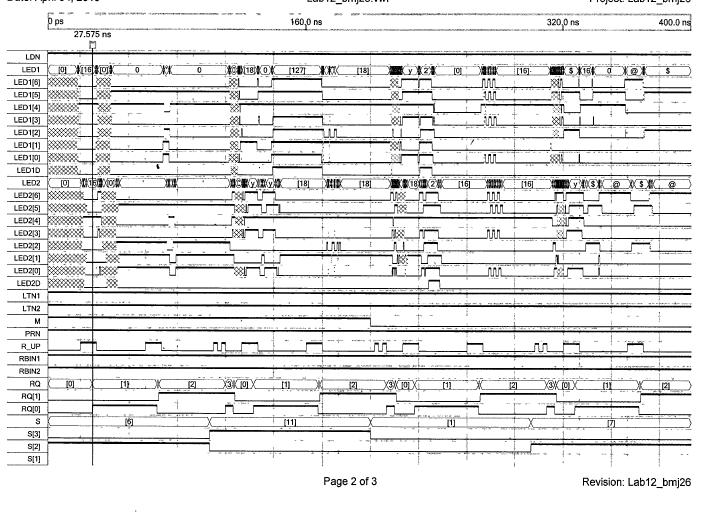
2 Callahan 2 d. We the double clicked the entry in Location column to choose the pin number on the FPGA chip. e. We repeated c and d for all of our pin assignments. 5. For the lab, we had to assign certain inputs and outputs to specific things. The inputs had to all be programmed to either toggle switches or pushbuttons along the bottom of the Altera DE2 board. The pushbuttons are normally high. We had to have the results outputted through two of the LEDs on the chip and we had to have the read and write addresses displayed by two LEDs. 6. With all of the pins assigned, it was time to upload the program to the FPGA for testing. We got an Altera DE2 board, an AC adapter for power, and a USB cable to connect the chip to the computer. We switched the RUN-PROG switch to the RUN position. In Quartus II, we choose Tools Programmer. We chose the FPGA as the hardware and chose JTAG mode. Finally, we clicked Add File to select our project.sof file and clicked start. We tested the FPGA to ensure functionality. 7. With the ALU circuit loaded and tested on the FPGA, we began to replace parts of the schematic with VHDL code. We began by generating the code for the decoder for the 7- segment displays. We deleted one of the 7-segment decoder from the schematic and replaced it with the DispBin.sym that we were given. Once we compiled and tested the new program, we replaced the other 7-segment decoder with the VHDL code. 8. Next, we edited the VHDL code for the decoders so that it shows the hexadecimal characters A, b, C, d, E, and F to represent 10 through 15. We then we re-simulated the ALU and verified operation on the FPGA. 9. With the decoder functioning, we replaced the 4x2:1 multiplexer, 4-bit latch, and address counters with VHDL that we wrote. We wrote the code, compiled it, created a symbol for it, and intergrated it into the circuitry. After each part was replaced, we tested the waveform, uploaded the code to the FPGA, and verified operation. Results For this lab, there are no circuit elements. The only thing used is an Altera DE2 board. We began by uploading the schematic and waveform from Lab 12. The circuit schematic is shown in Figure 1. The waveform is shown in Figure 2. Figure 1: This figure illustrates the schematic created in Quartus II from Lab 12.

3 Callahan 3

4 Callahan 4 Figure 2: These illustrates the circuit performing four different operations based on the schematic from Lab 12. With the files uploaded, we assigned the pins for the FPGA. Toggle switches were used for the following inputs: CLR, DN, L_EN, Din[3..0], S[3..0], Cn, M, and In_Sel. Pushbuttons were used for W_UP, R_UP, and W_EN. LEDs were used to display the write address and the read address. 7-segment LED displays were used to display the output of the register and the result of the ALU. Table 1 shows the inputs, signal names, pin numbers and pin descriptions for the FPGA. Input Signal Name Pin Number Pin Description CLR SW[0] PIN_N25 Toggle Switch[0] DN SW[1] PIN_N26 Toggle Switch[1] L_EN SW[2] PIN_P25 Toggle Switch[2] D[0] SW[3] PIN_AE14 Toggle Switch[3] D[1] SW[4] PIN_AF14 Toggle Switch[4] D[2] SW[5] PIN_AD13 Toggle Switch[5] D[3] SW[6] PIN_AC13 Toggle Switch[6] S[0] SW[7] PIN_C13 Toggle Switch[7] S[1] SW[8] PIN_B13 Toggle Switch[8] S[2] SW[9] PIN_A13 Toggle Switch[9] S[3] SW[10] PIN_N1 Toggle Switch[10] Cn SW[11 PIN_P1 Toggle Switch[11] M SW[12] PIN_P2 Toggle Switch[12] In_Sel SW[13] PIN_T7 Toggle Switch[13] W_UP KEY[0] PIN_O26 Pushbutton[0] R_UP KEY[1] PIN_N23 Pushbutton[1] W_EN KEY[2] PIN_P23 Pushbutton[2] LED1[0] HEX0[0] PIN_AF10 Seven Segment Digit 0[0] LED1[1] HEX0[1] PIN_AB12 Seven Segment Digit 0[1] LED1[2] HEX0[2] PIN_AC12 Seven Segment Digit 0[2] LED1[3] HEX0[3] PIN_AD11 Seven Segment Digit 0[3] LED1[4] HEX0[4] PIN_AE11 Seven Segment Digit 0[4] LED1[5] HEX0[5] PIN_V14 Seven Segment Digit 0[5] LED1[6] HEX0[6] PIN_V13 Seven Segment Digit 0[6] LED2[0] HEX1[0] PIN_V20 Seven Segment Digit 1[0] LED2[1] HEX1[1] PIN_V21 Seven Segment Digit 1[1] LED2[2] HEX1[2] PIN_W21 Seven Segment Digit 1[2]
5 Callahan 5 LED2[3] HEX1[3] PIN_Y22 Seven Segment Digit 1[3] LED2[4] HEX1[4] PIN_AA24 Seven Segment Digit 1[4] LED2[5] HEX1[5] PIN_AA23 Seven Segment Digit 1[5] LED2[6] HEX1[6] PIN_AB24 Seven Segment Digit 1[6] WQ[0] LEDG[7] PIN_Y18 LED Green[7] WQ[1] LEDG[8] PIN_Y12 LED Green[8] RQ[0] LEDG[5] PIN_U17 LED Green[5] RQ[1] LEDG[6] PIN_AA20 LED Green[6] Table 1: This table illustrates the inputs, signal names, pin numbers and pin descriptions for the FPGA. With the pin assignments completed, we began to replace parts of the schematic with the VHDL equivalent. We started by replacing the LED decoders with the VHDL given to us. The code is shown in Figure 3. We then modified the code so that the code displays hexadecimal characters. That code is shown in Figure 4. We tested the code after both changes and the waveform from Figure 2 did not change. Figure 3: This figure shows the original VHDL code for the LED decoder.
6 Callahan 6 Figure 4: This figure illustrates the VHDL code for the modified LED decoder. After we replaced the decoder, we wrote the VHDL code for the multiplexer. To write the code for the multiplexer, we first wrote code for one multiplexer and then wrote code for a 4x2:1 multiplexer. Figure 5 shows the code for the single multiplexer and Figure 6 shows the code for the implemented multiplexer. The waveform from Figure 2 did not change by implementing the VHDL code.


7 Callahan 7 Figure 5: This figure shows the VHDL code for a single multiplexer. Figure 6: This figure shows the VHDL code for the 4x2:1 multiplexer. Next we created the VHDL code for the 4-bit latch. We created the code for a single latch and implemented it in the code for a 4-bith latch. Figure 7 illustrates the code for the single latch and Figure 8 illustrates the code for the 4-bit latch. The schematic and the FPGA were tested and there was no change in the waveform from Figure 2 or with the functionality of the FPGA.


8 Callahan 8 Figure7: This figure shows the code for a single bit latch. Figure 8: This figure shows the VHDL code for the 4-bit latch. Finally, we created the VHDL code for the address counters. Figure 9 illustrates the code for the address counters. The schematic and the FPGA were tested and there was no change in the waveform from Figure 2 or with the functionality of the FPGA.
9 Callahan 9 Figure 9: This figure illustrates the VHDL code for the address counters. The final schematic that was uploaded to the FPGA is shown in Figure 10. The FPGA and the waveform shown in Figure 2 did not change functionality at any point of the changes. The waveforms were not shown after each testing in this report due to redundancy. Figure 10: This figure illustrates the final schematic with all of the VHDL equivalent circuits. Conclusion The purpose of this lab was to recreate an ALU by using an FPGA. To do so, we uploaded the schematic and waveform from Lab 12. We then assigned inputs and outputs of the schematic to the FPGA. We replaced parts of the program with VHDL code. After each part of the schematic was replaced, the waveform and the FPGA were tested to ensure functionality. In the end, the FPGA produced the same output as the ALU from Lab 12. Professor Helen Li s lecture slides References
10 Callahan 10 "Field Programmable Gate Array." Wikipedia. Wikimedia Foundation. Web. 19 Apr Lab Partner: Brandon Jones
Lab #13: FPGA Circuit Realization
 Lab #13: FPGA Circuit Realization ECE/COE 0501 Date of Experiment: 4/12/2017 Report Written: 4/17/2017 Submission Date: 4/19/2017 Nicholas Haver nicholas.haver@pitt.edu 1 H a v e r PURPOSE In this lab,
Lab #12: 4-Bit Arithmetic Logic Unit (ALU)
") Lab #12: 4-Bit Arithmetic Logic Unit (ALU) ECE/COE 0501 Date of Experiment: 4/3/2017 Report Written: 4/5/2017 Submission Date: 4/10/2017 Nicholas Haver nicholas.haver@pitt.edu 1 H a v e r PURPOSE The purpose
Lab #12: 4-Bit Arithmetic Logic Unit (ALU) ECE/COE 0501 Date of Experiment: 4/3/2017 Report Written: 4/5/2017 Submission Date: 4/10/2017 Nicholas Haver nicholas.haver@pitt.edu 1 H a v e r PURPOSE The purpose
STATIC RANDOM-ACCESS MEMORY
 STATIC RANDOM-ACCESS MEMORY by VITO KLAUDIO OCTOBER 10, 2015 CSC343 FALL 2015 PROF. IZIDOR GERTNER Table of contents 1. Objective... pg. 2 2. Functionality and Simulations... pg. 4 2.1 SR-LATCH... pg.
Laboratory Exercise 7
 Laboratory Exercise 7 Finite State Machines This is an exercise in using finite state machines. Part I We wish to implement a finite state machine (FSM) that recognizes two specific sequences of applied
California State University, Bakersfield Computer & Electrical Engineering & Computer Science ECE 3220: Digital Design with VHDL Laboratory 7
 California State University, Bakersfield Computer & Electrical Engineering & Computer Science ECE 322: Digital Design with VHDL Laboratory 7 Rational: The purpose of this lab is to become familiar in using
Laboratory Exercise 7
 Laboratory Exercise 7 Finite State Machines This is an exercise in using finite state machines. Part I We wish to implement a finite state machine (FSM) that recognizes two specific sequences of applied
HDL & High Level Synthesize (EEET 2035) Laboratory II Sequential Circuits with VHDL: DFF, Counter, TFF and Timer
 Laboratory II Sequential Circuits with VHDL: DFF, Counter, TFF and Timer") 1 P a g e HDL & High Level Synthesize (EEET 2035) Laboratory II Sequential Circuits with VHDL: DFF, Counter, TFF and Timer Objectives: Develop the behavioural style VHDL code for D-Flip Flop using gated,
1 P a g e HDL & High Level Synthesize (EEET 2035) Laboratory II Sequential Circuits with VHDL: DFF, Counter, TFF and Timer Objectives: Develop the behavioural style VHDL code for D-Flip Flop using gated,
Laboratory Exercise 6
 Laboratory Exercise 6 The purpose of this exercise is to investigate latches, flip-flops, and counters. Part I Altera FPGAs include flip-flops that are available for implementing a user s circuit. We will
Laboratory Exercise 3
 Laboratory Exercise 3 Latches, Flip-flops, and egisters The purpose of this exercise is to investigate latches, flip-flops, and registers. Part I Altera FPGAs include flip-flops that are available for
Ryerson University Department of Electrical and Computer Engineering COE/BME 328 Digital Systems
 1 P a g e Ryerson University Department of Electrical and Computer Engineering COE/BME 328 Digital Systems Lab 6 35 Marks (3 weeks) Design of a Simple General-Purpose Processor Due Date: Week 12 Objective:
CSCB58 - Lab 4. Prelab /3 Part I (in-lab) /1 Part II (in-lab) /1 Part III (in-lab) /2 TOTAL /8
 /1 Part II (in-lab) /1 Part III (in-lab) /2 TOTAL /8") CSCB58 - Lab 4 Clocks and Counters Learning Objectives The purpose of this lab is to learn how to create counters and to be able to control when operations occur when the actual clock rate is much faster.
CSCB58 - Lab 4 Clocks and Counters Learning Objectives The purpose of this lab is to learn how to create counters and to be able to control when operations occur when the actual clock rate is much faster.
Programmable Logic Design I
 Programmable Logic Design I Introduction In labs 11 and 12 you built simple logic circuits on breadboards using TTL logic circuits on 7400 series chips. This process is simple and easy for small circuits.
ELEC 204 Digital System Design LABORATORY MANUAL
 Elec 24: Digital System Design Laboratory ELEC 24 Digital System Design LABORATORY MANUAL : 4-bit hexadecimal Decoder & 4-bit Increment by N Circuit College of Engineering Koç University Important Note:
Lab #11: Register Files
 Lab #11: Register Files ECE/COE 0501 Date of Experiment: 3/20/2017 Report Written: 3/22/2017 Submission Date: 3/27/2017 Nicholas Haver nicholas.haver@pitt.edu 1 H a v e r PURPOSE The purpose of this lab
Electrical and Telecommunications Engineering Technology_TCET3122/TC520. NEW YORK CITY COLLEGE OF TECHNOLOGY The City University of New York
 NEW YORK CITY COLLEGE OF TECHNOLOGY The City University of New York DEPARTMENT: SUBJECT CODE AND TITLE: COURSE DESCRIPTION: REQUIRED: Electrical and Telecommunications Engineering Technology TCET 3122/TC
Lab 2: Hardware/Software Co-design with the Wimp51
 Lab 2: Hardware/Software Co-design with the Wimp51 CpE 214: Digital Engineering Lab II Last revised: February 26, 2013 (CAC) Hardware software co-design, now standard in industry, is an approach that brings
Lab #11: Register Files
 Lab #11: Register Files Zack Mattis Lab: 3/21/17 Report: 3/26/17 Partner: Brendan Schuster Purpose In this lab, 4x4 register was designed and fully implemented onto a protoboard that emulates the local
ET398 LAB 4. Concurrent Statements, Selection and Process
 ET398 LAB 4 Concurrent Statements, Selection and Process Decoders/Multiplexers February 16, 2013 Tiffany Turner OBJECTIVE The objectives of this lab were for us to become more adept at creating VHDL code
Main Design Project. The Counter. Introduction. Macros. Procedure
 Main Design Project Introduction In order to gain some experience with using macros we will exploit some of the features of our boards to construct a counter that will count from 0 to 59 with the counts
Why FPGAs? FPGA Overview. Why FPGAs?
 Transistor-level Logic Circuits Positive Level-sensitive EECS150 - Digital Design Lecture 3 - Field Programmable Gate Arrays (FPGAs) January 28, 2003 John Wawrzynek Transistor Level clk clk clk Positive
AN 848: Implementing Intel Cyclone 10 GX Triple-Rate SDI II with Nextera FMC Daughter Card Reference Design
 AN 848: Implementing Intel Cyclone 10 GX Triple-Rate SDI II with Nextera FMC Daughter Card Reference Design Updated for Intel Quartus Prime Design Suite: 18.0 Subscribe Send Feedback Latest document on
Step 1 - shaft decoder to generate clockwise/anticlockwise signals
 Workshop Two Shaft Position Encoder Introduction Some industrial automation applications require control systems which know the rotational position of a shaft. Similar devices are also used for digital
Main Design Project. The Counter. Introduction. Macros. Procedure
 Main Design Project Introduction In order to gain some experience with using macros we will exploit some of the features of our boards to construct a counter that will count from 0 to 59 with the counts
Lecture 10: Programmable Logic
 Lecture 10: Programmable Logic We ve spent the past couple of lectures going over some of the applications of digital logic And we can easily think of more useful things to do like having a 7-segment LED
University of Pennsylvania Department of Electrical and Systems Engineering. Digital Design Laboratory. Lab8 Calculator
 University of Pennsylvania Department of Electrical and Systems Engineering Digital Design Laboratory Purpose Lab Calculator The purpose of this lab is: 1. To get familiar with the use of shift registers
ENGG2410: Digital Design Lab 5: Modular Designs and Hierarchy Using VHDL
 ENGG2410: Digital Design Lab 5: Modular Designs and Hierarchy Using VHDL School of Engineering, University of Guelph Fall 2017 1 Objectives: Start Date: Week #7 2017 Report Due Date: Week #8 2017, in the
Microprocessor Design
 Microprocessor Design Principles and Practices With VHDL Enoch O. Hwang Brooks / Cole 2004 To my wife and children Windy, Jonathan and Michelle Contents 1. Designing a Microprocessor... 2 1.1 Overview
Digital Logic. ECE 206, Fall 2001: Lab 1. Learning Objectives. The Logic Simulator
 Learning Objectives ECE 206, : Lab 1 Digital Logic This lab will give you practice in building and analyzing digital logic circuits. You will use a logic simulator to implement circuits and see how they
Chapter 2. Digital Circuits
 Chapter 2. Digital Circuits Logic gates Flip-flops FF registers IC registers Data bus Encoders/Decoders Multiplexers Troubleshooting digital circuits Most contents of this chapter were covered in 88-217
IMPLEMENTATION OF A BINARY SELECTION SYSTEM CREATED IN XILINX USING FPGA
 ANNALS of Faculty Engineering Hunedoara International Journal of Engineering Tome XV [2017] Fascicule 3 [August] ISSN: 1584-2665 [print; online] ISSN: 1584-2673 [CD-Rom; online] a free-access multidisciplinary
EEM Digital Systems II
 ANADOLU UNIVERSITY DEPARTMENT OF ELECTRICAL AND ELECTRONICS ENGINEERING EEM 334 - Digital Systems II LAB 3 FPGA HARDWARE IMPLEMENTATION Purpose In the first experiment, four bit adder design was prepared
Laboratory 4. Figure 1: Serdes Transceiver
 Laboratory 4 The purpose of this laboratory exercise is to design a digital Serdes In the first part of the lab, you will design all the required subblocks for the digital Serdes and simulate them In part
CHAPTER 3 EXPERIMENTAL SETUP
 CHAPTER 3 EXPERIMENTAL SETUP In this project, the experimental setup comprised of both hardware and software. Hardware components comprised of Altera Education Kit, capacitor and speaker. While software
DALHOUSIE UNIVERSITY Department of Electrical & Computer Engineering Digital Circuits - ECED 2200
 DALHOUSIE UNIVERSITY Department of Electrical & Computer Engineering Digital Circuits - ECED 2200 Tutorial 1. Xilinx Integrated Software Environment (ISE) Tools Objectives: 1. Familiarize yourself with
LAB 3 Verilog for Combinational Circuits
 Goals To Do LAB 3 Verilog for Combinational Circuits Learn how to implement combinational circuits using Verilog. Design and implement a simple circuit that controls the 7-segment display to show a 4-bit
Elwin Cabrera May 11, 2016 DIGITAL CLOCK. ECE271/CSC222 Final Project Report
 Elwin Cabrera May 11, 2016 DIGITAL CLOCK ECE271/CSC222 Final Project Report Problem Specification: For our CSC222/ECE271 final, we had to design a digital clock. We had to use Quartus and design a control
EET 1131 Lab #10 Latches and Flip-Flops
 Name OBJECTIVES: 1. To study the operation of a D latch. 2. To study the operation of a D flip-flop. 3. To study the operation of a J-K flip-flop. EQUIPMENT REQUIRED: Safety glasses ICs: 7474, 7475, 74LS76
Digital Fundamentals. Lab 5 Latches & Flip-Flops CETT Name: Date:
 Richland College School of Engineering & Technology Rev. 0 B. Donham Rev. 1 (7/2003) J. Horne Rev. 2 (1/2008) J. Bradbury Rev. 3 (7/2015) J. Bradbury Digital Fundamentals CETT 1425 Lab 5 Latches & Flip-Flops
Laboratory Exercise 4
 Laboratory Exercise 4 Polling and Interrupts The purpose of this exercise is to learn how to send and receive data to/from I/O devices. There are two methods used to indicate whether or not data can be
Ryerson University Department of Electrical and Computer Engineering EES508 Digital Systems
 1 P a g e Ryerson University Department of Electrical and Computer Engineering EES508 Digital Systems Lab 5 - VHDL for Sequential Circuits: Implementing a customized State Machine 15 Marks ( 2 weeks) Due
Lab 17: Building a 4-Digit 7-Segment LED Decoder
 Phys2303 L.A. Bumm [Basys3 1.2.1] Lab 17 (p1) Lab 17: Building a 4-Digit 7-Segment LED Decoder In this lab you will make 5 test circuits in addition to the 4-digit 7-segment decoder. The test circuits
EET 1131 Lab #12 - Page 1 Revised 8/10/2018
 Name EET 1131 Lab #12 Shift Registers Equipment and Components Safety glasses ETS-7000 Digital-Analog Training System Integrated Circuits: 74164, 74195 Quartus II software and Altera DE2-115 board Shift
CHAPTER 4 RESULTS & DISCUSSION
 CHAPTER 4 RESULTS & DISCUSSION 3.2 Introduction This project aims to prove that Modified Baugh-Wooley Two s Complement Signed Multiplier is one of the high speed multipliers. The schematic of the multiplier
CPSC 121: Models of Computation Lab #5: Flip-Flops and Frequency Division
 CPSC 121: Models of Computation Lab #5: Flip-Flops and Frequency Division Objectives In this lab, we will see the sequential circuits latches and flip-flops. Latches and flip-flops can be used to build
IS1500 (not part of IS1200) Logic Design Lab (LD-Lab)
 Logic Design Lab (LD-Lab)") Introduction IS1500 (not part of IS1200) Logic Design Lab (LD-Lab) 2017-10-26 The purpose of this lab is to give a hands-on experience of using gates and digital building blocks. These build blocks are
Introduction IS1500 (not part of IS1200) Logic Design Lab (LD-Lab) 2017-10-26 The purpose of this lab is to give a hands-on experience of using gates and digital building blocks. These build blocks are
Digital Fundamentals: A Systems Approach
 Digital Fundamentals: A Systems Approach Counters Chapter 8 A System: Digital Clock Digital Clock: Counter Logic Diagram Digital Clock: Hours Counter & Decoders Finite State Machines Moore machine: One
PHYSICS 5620 LAB 9 Basic Digital Circuits and Flip-Flops
 PHYSICS 5620 LAB 9 Basic Digital Circuits and Flip-Flops Objective Construct a two-bit binary decoder. Study multiplexers (MUX) and demultiplexers (DEMUX). Construct an RS flip-flop from discrete gates.
NORTHWESTERN UNIVERSITY TECHNOLOGICAL INSTITUTE
 NORTHWESTERN UNIVERSITY TECHNOLOGICL INSTITUTE ECE 270 Experiment #8 DIGITL CIRCUITS Prelab 1. Draw the truth table for the S-R Flip-Flop as shown in the textbook. Draw the truth table for Figure 7. 2.
Table of Contents Introduction
 Page 1/9 Waveforms 2015 tutorial 3-Jan-18 Table of Contents Introduction Introduction to DAD/NAD and Waveforms 2015... 2 Digital Functions Static I/O... 2 LEDs... 2 Buttons... 2 Switches... 2 Pattern Generator...
Advanced Devices. Registers Counters Multiplexers Decoders Adders. CSC258 Lecture Slides Steve Engels, 2006 Slide 1 of 20
 Advanced Devices Using a combination of gates and flip-flops, we can construct more sophisticated logical devices. These devices, while more complex, are still considered fundamental to basic logic design.
Altera s Max+plus II Tutorial
 Altera s Max+plus II Tutorial Written by Kris Schindler To accompany Digital Principles and Design (by Donald D. Givone) 8/30/02 1 About Max+plus II Altera s Max+plus II is a powerful simulation package
CPSC 121: Models of Computation Lab #5: Flip-Flops and Frequency Division
 CPSC 121: Models of Computation Lab #5: Flip-Flops and Frequency Division Objectives In this lab, you will see two types of sequential circuits: latches and flip-flops. Latches and flip-flops can be used
Experiment # 4 Counters and Logic Analyzer
 EE20L - Introduction to Digital Circuits Experiment # 4. Synopsis: Experiment # 4 Counters and Logic Analyzer In this lab we will build an up-counter and a down-counter using 74LS76A - Flip Flops. The
CPE 200L LABORATORY 3: SEQUENTIAL LOGIC CIRCUITS UNIVERSITY OF NEVADA, LAS VEGAS GOALS: BACKGROUND: SR FLIP-FLOP/LATCH
 CPE 200L LABORATORY 3: SEUENTIAL LOGIC CIRCUITS DEPARTMENT OF ELECTRICAL AND COMPUTER ENGINEERING UNIVERSITY OF NEVADA, LAS VEGAS GOALS: Learn to use Function Generator and Oscilloscope on the breadboard.
Laboratory 1 - Introduction to Digital Electronics and Lab Equipment (Logic Analyzers, Digital Oscilloscope, and FPGA-based Labkit)
") Massachusetts Institute of Technology Department of Electrical Engineering and Computer Science 6. - Introductory Digital Systems Laboratory (Spring 006) Laboratory - Introduction to Digital Electronics
Massachusetts Institute of Technology Department of Electrical Engineering and Computer Science 6. - Introductory Digital Systems Laboratory (Spring 006) Laboratory - Introduction to Digital Electronics
Objectives. Combinational logics Sequential logics Finite state machine Arithmetic circuits Datapath
 Objectives Combinational logics Sequential logics Finite state machine Arithmetic circuits Datapath In the previous chapters we have studied how to develop a specification from a given application, and
Circuit and System Design for DSP
 lektronik abor Circuit and System Design for DSP Prof. Dr. Martin J. W. Schubert, Electronics Laboratory, OTH Regensburg, Regensburg, Germany Circuit and System Design for DSP Principles and Practices
YEDITEPE UNIVERSITY DEPARTMENT OF COMPUTER ENGINEERING. EXPERIMENT VIII: FLIP-FLOPS, COUNTERS 2014 Fall
 YEDITEPE UNIVERSITY DEPARTMENT OF COMPUTER ENGINEERING EXPERIMENT VIII: FLIP-FLOPS, COUNTERS 2014 Fall Objective: - Dealing with the operation of simple sequential devices. Learning invalid condition in
Lab #10 Hexadecimal-to-Seven-Segment Decoder, 4-bit Adder-Subtractor and Shift Register. Fall 2017
 University of Texas at El Paso Electrical and Computer Engineering Department EE 2169 Laboratory for Digital Systems Design I Lab #10 Hexadecimal-to-Seven-Segment Decoder, 4-bit Adder-Subtractor and Shift
DE2 Electronic Keyboard with the Autoplayer Feature ReadMeFirst
 Lab Summary DE2 Electronic Keyboard with the Autoplayer Feature ReadMeFirst At the end of this lab your ever expanding circuit design will automatically play an entire song stored in read only memory.
Using SignalTap II in the Quartus II Software
 White Paper Using SignalTap II in the Quartus II Software Introduction The SignalTap II embedded logic analyzer, available exclusively in the Altera Quartus II software version 2.1, helps reduce verification
DALHOUSIE UNIVERSITY Department of Electrical & Computer Engineering Digital Circuits - ECED 220. Experiment 4 - Latches and Flip-Flops
 DLHOUSIE UNIVERSITY Department of Electrical & Computer Engineering Digital Circuits - ECED 0 Experiment - Latches and Flip-Flops Objectives:. To implement an RS latch memory element. To implement a JK
CSE 352 Laboratory Assignment 3
 CSE 352 Laboratory Assignment 3 Introduction to Registers The objective of this lab is to introduce you to edge-trigged D-type flip-flops as well as linear feedback shift registers. Chapter 3 of the Harris&Harris
Debugging of VHDL Hardware Designs on Altera s DE2 Boards
 Debugging of VHDL Hardware Designs on Altera s DE2 Boards This tutorial presents some basic debugging concepts that can be helpful in creating VHDL designs for implementation on Altera s DE2 boards. It
Rensselaer Polytechnic Institute Computer Hardware Design ECSE Report. Lab Three Xilinx Richards Controller and Logic Analyzer Laboratory
 RPI Rensselaer Polytechnic Institute Computer Hardware Design ECSE 4770 Report Lab Three Xilinx Richards Controller and Logic Analyzer Laboratory Name: Walter Dearing Group: Brad Stephenson David Bang
FPGA-BASED EDUCATIONAL LAB PLATFORM
 FPGA-BASED EDUCATIONAL LAB PLATFORM Mircea Alexandru DABÂCAN, Clint COLE Mircea Dabâcan is with Technical University of Cluj-Napoca, Electronics and Telecommunications Faculty, Applied Electronics Department,
Lab #5: Design Example: Keypad Scanner and Encoder - Part 1 (120 pts)
") Nate Pihlstrom, npihlstr@uccs.edu Lab #5: Design Example: Keypad Scanner and Encoder - Part 1 (120 pts) Objective The objective of lab assignments 5 through 9 are to systematically design and implement
Nate Pihlstrom, npihlstr@uccs.edu Lab #5: Design Example: Keypad Scanner and Encoder - Part 1 (120 pts) Objective The objective of lab assignments 5 through 9 are to systematically design and implement
3/5/2017. A Register Stores a Set of Bits. ECE 120: Introduction to Computing. Add an Input to Control Changing a Register s Bits
 University of Illinois at Urbana-Champaign Dept. of Electrical and Computer Engineering ECE 120: Introduction to Computing Registers A Register Stores a Set of Bits Most of our representations use sets
Chapter 7 Counters and Registers
 Chapter 7 Counters and Registers Chapter 7 Objectives Selected areas covered in this chapter: Operation & characteristics of synchronous and asynchronous counters. Analyzing and evaluating various types
Design of a Binary Number Lock (using schematic entry method) 1. Synopsis: 2. Description of the Circuit:
 1. Synopsis: 2. Description of the Circuit:") Design of a Binary Number Lock (using schematic entry method) 1. Synopsis: This lab gives you more exercise in schematic entry, state machine design using the one-hot state method, further understanding
Design of a Binary Number Lock (using schematic entry method) 1. Synopsis: This lab gives you more exercise in schematic entry, state machine design using the one-hot state method, further understanding
COMPUTER ENGINEERING PROGRAM
 COMPUTER ENGINEERING PROGRAM California Polytechnic State University CPE 169 Experiment 6 Introduction to Digital System Design: Combinational Building Blocks Learning Objectives 1. Digital Design To understand
March 13, :36 vra80334_appe Sheet number 1 Page number 893 black. appendix. Commercial Devices
 March 13, 2007 14:36 vra80334_appe Sheet number 1 Page number 893 black appendix E Commercial Devices In Chapter 3 we described the three main types of programmable logic devices (PLDs): simple PLDs, complex
Debugging of Verilog Hardware Designs on Altera s DE-Series Boards. 1 Introduction. For Quartus Prime 15.1
 Debugging of Verilog Hardware Designs on Altera s DE-Series Boards For Quartus Prime 15.1 1 Introduction This tutorial presents some basic debugging concepts that can be helpful in creating Verilog designs
DIGITAL CIRCUIT LOGIC UNIT 9: MULTIPLEXERS, DECODERS, AND PROGRAMMABLE LOGIC DEVICES
 DIGITAL CIRCUIT LOGIC UNIT 9: MULTIPLEXERS, DECODERS, AND PROGRAMMABLE LOGIC DEVICES 1 Learning Objectives 1. Explain the function of a multiplexer. Implement a multiplexer using gates. 2. Explain the
FPGA Design. Part I - Hardware Components. Thomas Lenzi
 FPGA Design Part I - Hardware Components Thomas Lenzi Approach We believe that having knowledge of the hardware components that compose an FPGA allow for better firmware design. Being able to visualise
Digital. Digital. Revision: v0.19 Date: : / 76
 Digital Revision: v0.19 Date: 2018-06-14 07:01 https://github.com/hneemann/digital 1 / 76 Table of Contents A General 1. Digital...5 1.1. Introduction... 5 1.2. First Steps...5 1.3. Wires...13 1.4. Hierarchical
Field Programmable Gate Arrays (FPGAs)
") Field Programmable Gate Arrays (FPGAs) Introduction Simulations and prototyping have been a very important part of the electronics industry since a very long time now. Before heading in for the actual
Field Programmable Gate Arrays (FPGAs) Introduction Simulations and prototyping have been a very important part of the electronics industry since a very long time now. Before heading in for the actual
COMP2611: Computer Organization Building Sequential Logics with Logisim
 1 COMP2611: Computer Organization Building Sequential Logics with COMP2611 Fall2015 Overview 2 You will learn the following in this lab: building a SR latch on, building a D latch on, building a D flip-flop
Lab #10: Building Output Ports with the 6811
 1 Tiffany Q. Liu April 11, 2011 CSC 270 Lab #10 Lab #10: Building Output Ports with the 6811 Introduction The purpose of this lab was to build a 1-bit as well as a 2-bit output port with the 6811 training
Inside Digital Design Accompany Lab Manual
 1 Inside Digital Design, Accompany Lab Manual Inside Digital Design Accompany Lab Manual Simulation Prototyping Synthesis and Post Synthesis Name- Roll Number- Total/Obtained Marks- Instructor Signature-
COE328 Course Outline. Fall 2007
 COE28 Course Outline Fall 2007 1 Objectives This course covers the basics of digital logic circuits and design. Through the basic understanding of Boolean algebra and number systems it introduces the student
Fundamentals of Digital Electronics
 Fundamentals of Digital Electronics by Professor Barry Paton Dalhousie University March 998 Edition Part Number 32948A- Fundamentals of Digital Electronics Copyright Copyright 998 by National Instruments
Tutorial 11 ChipscopePro, ISE 10.1 and Xilinx Simulator on the Digilent Spartan-3E board
 Tutorial 11 ChipscopePro, ISE 10.1 and Xilinx Simulator on the Digilent Spartan-3E board Introduction This lab will be an introduction on how to use ChipScope for the verification of the designs done on
ECE 270 Lab Verification / Evaluation Form. Experiment 8
 ECE 270 Lab Verification / Evaluation Form Experiment 8 Evaluation: IMPORTANT! You must complete this experiment during your scheduled lab period. All work for this experiment must be demonstrated to and
4.1* Combinational logic circuits implement logic functions using a combination of logic gates. Recall
 CALIFORNIA STATE UNIVERSITY LOS ANGELES Department of Electrical and Computer Engineering EE-2449 Digital Logic Lab EXPERIMENT 4 LOGIC FUNCTIONS Text: Mano and Ciletti, Digital Design, 5 th Edition, Chapter
CSE140L: Components and Design Techniques for Digital Systems Lab. CPU design and PLDs. Tajana Simunic Rosing. Source: Vahid, Katz
 CSE140L: Components and Design Techniques for Digital Systems Lab CPU design and PLDs Tajana Simunic Rosing Source: Vahid, Katz 1 Lab #3 due Lab #4 CPU design Today: CPU design - lab overview PLDs Updates
Encoders and Decoders: Details and Design Issues
 Encoders and Decoders: Details and Design Issues Edward L. Bosworth, Ph.D. TSYS School of Computer Science Columbus State University Columbus, GA 31907 bosworth_edward@colstate.edu Slide 1 of 25 slides
Chapter Contents. Appendix A: Digital Logic. Some Definitions
 A- Appendix A - Digital Logic A-2 Appendix A - Digital Logic Chapter Contents Principles of Computer Architecture Miles Murdocca and Vincent Heuring Appendix A: Digital Logic A. Introduction A.2 Combinational
EE292: Fundamentals of ECE
 EE292: Fundamentals of ECE Fall 2012 TTh 10:00-11:15 SEB 1242 Lecture 23 121120 http://www.ee.unlv.edu/~b1morris/ee292/ 2 Outline Review Combinatorial Logic Sequential Logic 3 Combinatorial Logic Circuits
Laboratory Manual and Supplementary Notes. ECE 495: Computer Engineering Design Laboratory
 Laboratory Manual and Supplementary Notes ECE 495: Computer Engineering Design Laboratory Version 3 Jason Koonts Dr. Edwin Hou Department of Electrical and Computer Engineering New Jersey Institute of
Logic Devices for Interfacing, The 8085 MPU Lecture 4
 Logic Devices for Interfacing, The 8085 MPU Lecture 4 1 Logic Devices for Interfacing Tri-State devices Buffer Bidirectional Buffer Decoder Encoder D Flip Flop :Latch and Clocked 2 Tri-state Logic Outputs
The basic logic gates are the inverter (or NOT gate), the AND gate, the OR gate and the exclusive-or gate (XOR). If you put an inverter in front of
, the AND gate, the OR gate and the exclusive-or gate (XOR). If you put an inverter in front of") 1 The basic logic gates are the inverter (or NOT gate), the AND gate, the OR gate and the exclusive-or gate (XOR). If you put an inverter in front of the AND gate, you get the NAND gate etc. 2 One of the
1 The basic logic gates are the inverter (or NOT gate), the AND gate, the OR gate and the exclusive-or gate (XOR). If you put an inverter in front of the AND gate, you get the NAND gate etc. 2 One of the
Sequential Design Basics
 Sequential Design Basics Lecture 2 topics A review of devices that hold state A review of Latches A review of Flip-Flops Unit of text Set-Reset Latch/Flip-Flops/D latch/ Edge triggered D Flip-Flop 8/22/22
1. Synopsis: 2. Description of the Circuit:
 Design of a Binary Number Lock (using schematic entry method) 1. Synopsis: This lab gives you more exercise in schematic entry, state machine design using the one-hot state method, further understanding
Physics 323. Experiment # 10 - Digital Circuits
 Physics 323 Experiment # 10 - Digital Circuits Purpose This is a brief introduction to digital (logic) circuits using both combinational and sequential logic. The basic building blocks will be the Transistor
FPGA TechNote: Asynchronous signals and Metastability
 FPGA TechNote: Asynchronous signals and Metastability This Doulos FPGA TechNote gives a brief overview of metastability as it applies to the design of FPGAs. The first section introduces metastability
MUHAMMAD NAEEM LATIF MCS 3 RD SEMESTER KHANEWAL
 1. A stage in a shift register consists of (a) a latch (b) a flip-flop (c) a byte of storage (d) from bits of storage 2. To serially shift a byte of data into a shift register, there must be (a) one click
IE1204 Digital Design. F11: Programmable Logic, VHDL for Sequential Circuits. Masoumeh (Azin) Ebrahimi
 Ebrahimi") IE1204 Digital Design F11: Programmable Logic, VHDL for Sequential Circuits Masoumeh (Azin) Ebrahimi (masebr@kth.se) Elena Dubrova (dubrova@kth.se) KTH / ICT / ES This lecture BV pp. 98-118, 418-426, 507-519
IE1204 Digital Design F11: Programmable Logic, VHDL for Sequential Circuits Masoumeh (Azin) Ebrahimi (masebr@kth.se) Elena Dubrova (dubrova@kth.se) KTH / ICT / ES This lecture BV pp. 98-118, 418-426, 507-519
Spartan-II Development System
 2002-May-4 Introduction Dünner Kirchweg 77 32257 Bünde Germany www.trenz-electronic.de The Spartan-II Development System is designed to provide a simple yet powerful platform for FPGA development, which
Figure 1 Block diagram of a 4-bit binary counter
 Lab 3: Four-Bit Binary Counter EE-459/500 HDL Based Digital Design with Programmable Logic Electrical Engineering Department, University at Buffalo Last update: Cristinel Ababei, August 2012 1. Objective