Department of CSIT. Class: B.SC Semester: II Year: 2013 Paper Title: Introduction to logics of Computer Max Marks: 30
|
|
|
- Claude Dixon
- 6 years ago
- Views:
Transcription
1 Department of CSIT Class: B.SC Semester: II Year: 2013 Paper Title: Introduction to logics of Computer Max Marks: 30 Section A: (All 10 questions compulsory) 10X1=10 Very Short Answer Questions: Write Very short answers to following questions Q1. What is Gate? Explain in brief. Electronic digital circuits are also called logic circuits because, with the proper input, they establish logical manipulation paths. Any desired information for computing or control can be operated upon by passing binary signals through various combinations of logic circuits, each signal representing a variable and carrying one bit of information. Logic circuits that perform the logical operations of AND, OR, and NOT. These circuits, called gates, are blocks of hardware that produce a logic-lor logic-o output signal if input logic requirements are satisfied. Q2. Write advantages of Binary coded decimal? 1. One advantage of BCD over binary representations is that there is no limit to the size of a number. To add another digit, just add a new 4-bit sequence. 2. Numbers represented in pure binary format are limited to the largest number that can be represented by 8, 16, 32 or 64 bits. 3. It is easier to convert decimal numbers to and from BCD than binary and, though BCD is often converted to binary for arithmetic processing, it is possible to build hardware that operates directly on BCD. Q3. How SOP of any boolean function is creates? The sum of products is a Boolean expression containing AND terms, called product terms, of one or more literals each. The sum denotes the ORing of these terms. An example of a function expressed in sum of products is F = y' + xy + x'yz' The expression has three product terms of one, two, and three literals each, respectively. Their sum is in effect an OR operation Q4. Represent Exclusive NOR Gate with its truth table.
2 Q5. Describe Standard Sum of Boolean variables? The n Binary variables forming an OR term, with each variable being primed if the corresponding bit of the binary number is 1 or unprimed if the corresponding bit of the binary number is 0, provide 2" possible combinations, called maxterms, or standard sums. For e.g. Q6. Demonstrate associative Law Associative law. A binary operator * on a set S is said to be associative whenever (x * y) * z = x * (y * z) for all x, y, z, E S Q7. Explain asynchronous sequential circuit system ANS : The digital circuit are mainly categorised into two types: (i) Combinational circuit and, (ii) Sequential circuit every digital system is likely to have combinational circuits, most systems encountered in practice also include memory elements, which require that the system be described in terms of sequential Logic. There are two main types of sequential circuits. Their classification depends on the timing of their signals, they are: Synchronous and asynchronous sequential circuit. The behavior of an asynchronous sequential circuit depends upon the order in which its input signals change and can be affected at any instant of time. The memory elements commonly used in asynchronous sequential circuits are time-delay devices. The memory capability of a time-delay device is due to the finite time it takes for the signal to propagate through the device. Q8. Define Shift Registers. Ans: A register capable of shifting its binary information either to the right or to the left is called a shift register. The logical configuration of a shift register consists of a chain of flip-flops connected in cascade, with the output of one flip-flop connected to the input of the next flip-flop. All flip-flops receive a common clock pulse that causes the shift from one stage to the next.
3 Q9. Represent in minterm form f(x,y,z)=σ(1,3,5,7) Ans: f(x,y,z) = m 1 + m 3 + m 5 + m 7 Q10. Prove x.x=x by using Boolean algebra postulates.
 10 s (2) 9 s Complement:")
4 Section B: (Attempt any 4 questions out of 6 questions) 4X5=20 Descriptive Questions: Q11. Perform the subtraction of decimal numbers using (1) 10 s (2) 9 s Complement:

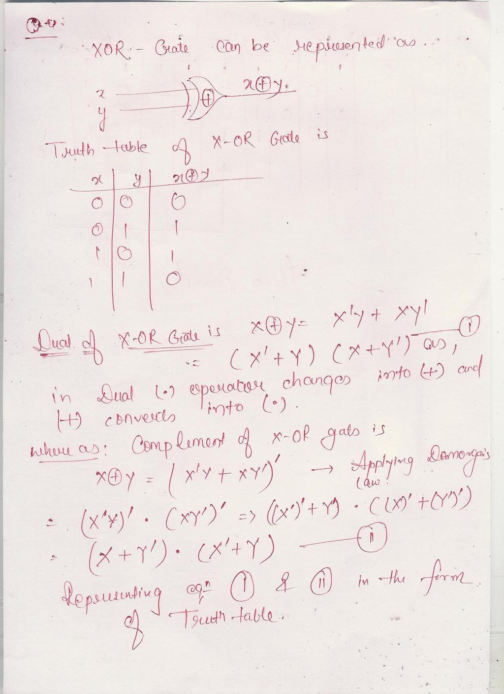
5 Q12. Implement the Boolean function with AND, OR and NOT gates F= xy + x'y' +y'z. Q13. Show that dual of the X-OR gate s equal to its complement.
6


7 Q14. Simplify the Boolean function using MAP method: F= A'C + A'B + AB'C + BC Q15. Design the combinational circuit that accepts a 3-bit number and generates an output binary number equal to the square of the input number. Ans: The First Step in the design is to drive the truth table of combinational circuit. Firstly we design the truth table with three input and six output are needed to accommodate all possible combinations of binary numbers. Truth
8 table and circuit diagram are described as follows: where, A 0, A 1, A 2 are act as input and B 0, B 1, B 2, B 3, B 4, B 5 are act as output Q16. What is sequential circuit? Compare Combinational and sequential circuit. Ans: The digital circuit are mainly categorised into two types: (i) Combinational circuit and, (ii) Sequential circuit every digital system is likely to have combinational circuits, most systems encountered in practice also include memory elements, which require that the system be described in terms of sequential Logic. The memory elements are devices capable of storing binary information within them. The binary information stored in the memory elements at any given time defines the state of the sequential circuit. The sequential circuit receives binary information from external inputs. These inputs, together with the present state of the memory elements, determine the binary value at the output terminals. They also determine the condition for changing the state in the memory elements. BLOCK DIAGRAM OF SEQUENTIAL CIRCUIT The block diagram demonstrates that the external outputs in a sequential circuit are a function not only of external inputs, but also of the present state of the memory elements. The next state of the memory elements is also a function of
9 external inputs and the present state. Thus, a sequential circuit is specified by a time sequence of inputs, outputs, and internal states. Comparison of Combinational and Sequential circuit S.NO Combinational Cicuit Sequential Circuit 1. A combinational circuit can be defined as a circuit whose output is dependent only on the inputs at the same instant of time a sequential circuit can be defined as a circuit whose output depends not only on the present inputs but also on the past history of inputs. 2. For a combinational circuit, the values of the variable are usually For a sequential circuit, the values of the variable are usually specified specified over the whole at certain discrete time instants continuous time. 3. It contains no memory elements It contains memory elements 4. The present value of it s outputs are determined solely by the present values of it s inputs The present value of it s outputs are determined by the present value of it s inputs and it s past state 5. It s behavior is described by the set of output functions 6. HalfAdder, FullAdder, Half Subtractor, Full Subtractor are examples of combinational circuits It s behavior is described by the set of next-state(memory) functions and the set of output functions Flip-Flops, Counters form the sequential circuit. Q17. What is Synchronous Counter? Explain in brief. Ans: A sequential circuit that goes through a prescribed sequence of states upon the application of input pulses is called a counter. The input pulses, called count pulses, may be clock pulses or they may originate from an external source and may occur at prescribed intervals of time or at random. In a counter, the sequence of states may follow a binary count or any other sequence of states. Counters are found in almost all equipment containing digital logic. They are used for counting the number of occurrences of an event and are useful for generating timing sequences to control operations in a digital system. In general there are two types of counter, asynchronous counter and Synchronous counter. In asynchronous counter, the flip-flop output transition serves as a source for triggering other flipflops. In other words, the CP inputs of all flip-flops (except the first) are triggered not by the incoming pulses, but rather by the transition that occurs in other flip-flops. In synchronous counter, the input pulses are applied to all CP inputs of all flip-flops. The change of state of a particular flip-flop is dependent on the present state of other flipflops.
10 Designing of Synchronous counter: The most simplest synchronous counter is Binary counter: A counter that follows the binary sequence is called a binary counter. An n-bit binary counter consists of n flip-flops and can count in binary from 0 to 2" 1. The state transitions in clocked sequential circuits occur during a clock pulse; the flipflops remain in their present states if no pulse occurs. The next state of a counter depends entirely on its present state, and the state transition occurs every time the pulse occurs. For example: State Diagram of 3-bit binary counter The three flip-flops are given variable designations A" A" and Ao. Binary counters are most efficiently constructed with T flip-flops (or JK flip-flops with J and K tied together). The flip-flop excitation for the T inputs is derived from the excitation table of the T flip-flop and from inspection of the state transition of the present state to the next state. consider the flip-flop input entries for row 001. The present state here is OOI and the next state is 0 I 0, which is the next count in the sequence. Comparing these two counts, we note that A, goes from 0 to 0; so TA, is marked with a 0 because flip-flop A2 must remain unchanged when a clock pulse occurs. Al goes from 0 to I; so TA, is marked with a I because this flip-flop must be complemented in the next clock pulse. Similarly, Ao goes from I to 0, indicating that it must be complemented; so TAo is marked with a 1. The last row with present state III is compared with the first count 000, which is its next state. Going from all 1 s to all O's requires that all three flipflops be complemented. MAPS for 3-bit Binary Counter
11 The flip-flop input functions from the excitation tables are simplified in the maps. The Boolean functions listed under each map specify the combinational circuit part of the counter. Including these functions with the three flip-flops, we obtain the logic diagram of the binary synchronous counter.
The word digital implies information in computers is represented by variables that take a limited number of discrete values.
 Class Overview Cover hardware operation of digital computers. First, consider the various digital components used in the organization and design. Second, go through the necessary steps to design a basic
Find the equivalent decimal value for the given value Other number system to decimal ( Sample)
") VELAMMAL COLLEGE OF ENGINEERING AND TECHNOLOGY, MADURAI 65 009 Department of Information Technology Model Exam-II-Question bank PART A (Answer for all Questions) (8 X = 6) K CO Marks Find the equivalent
VELAMMAL COLLEGE OF ENGINEERING AND TECHNOLOGY, MADURAI 65 009 Department of Information Technology Model Exam-II-Question bank PART A (Answer for all Questions) (8 X = 6) K CO Marks Find the equivalent
Registers and Counters
 Registers and Counters Clocked sequential circuit = F/Fs and combinational gates Register Group of flip-flops (share a common clock and capable of storing one bit of information) Consist of a group of
Registers and Counters
 Registers and Counters Clocked sequential circuit = F/Fs and combinational gates Register Group of flip-flops (share a common clock and capable of storing one bit of information) Consist of a group of
MC9211 Computer Organization
 MC9211 Computer Organization Unit 2 : Combinational and Sequential Circuits Lesson2 : Sequential Circuits (KSB) (MCA) (2009-12/ODD) (2009-10/1 A&B) Coverage Lesson2 Outlines the formal procedures for the
1. Convert the decimal number to binary, octal, and hexadecimal.
 1. Convert the decimal number 435.64 to binary, octal, and hexadecimal. 2. Part A. Convert the circuit below into NAND gates. Insert or remove inverters as necessary. Part B. What is the propagation delay
UNIT 1: DIGITAL LOGICAL CIRCUITS What is Digital Computer? OR Explain the block diagram of digital computers.
 UNIT 1: DIGITAL LOGICAL CIRCUITS What is Digital Computer? OR Explain the block diagram of digital computers. Digital computer is a digital system that performs various computational tasks. The word DIGITAL
Solution to Digital Logic )What is the magnitude comparator? Design a logic circuit for 4 bit magnitude comparator and explain it,
What is the magnitude comparator? Design a logic circuit for 4 bit magnitude comparator and explain it,") Solution to Digital Logic -2067 Solution to digital logic 2067 1.)What is the magnitude comparator? Design a logic circuit for 4 bit magnitude comparator and explain it, A Magnitude comparator is a combinational
Solution to Digital Logic -2067 Solution to digital logic 2067 1.)What is the magnitude comparator? Design a logic circuit for 4 bit magnitude comparator and explain it, A Magnitude comparator is a combinational
Department of Computer Science and Engineering Question Bank- Even Semester:
 Department of Computer Science and Engineering Question Bank- Even Semester: 2014-2015 CS6201& DIGITAL PRINCIPLES AND SYSTEM DESIGN (Common to IT & CSE, Regulation 2013) UNIT-I 1. Convert the following
MODULE 3. Combinational & Sequential logic
 MODULE 3 Combinational & Sequential logic Combinational Logic Introduction Logic circuit may be classified into two categories. Combinational logic circuits 2. Sequential logic circuits A combinational
CHAPTER 4: Logic Circuits
 CHAPTER 4: Logic Circuits II. Sequential Circuits Combinational circuits o The outputs depend only on the current input values o It uses only logic gates, decoders, multiplexers, ALUs Sequential circuits
Synchronous Sequential Logic
 Synchronous Sequential Logic -A Sequential Circuit consists of a combinational circuit to which storage elements are connected to form a feedback path. The storage elements are devices capable of storing
EE292: Fundamentals of ECE
 EE292: Fundamentals of ECE Fall 2012 TTh 10:00-11:15 SEB 1242 Lecture 23 121120 http://www.ee.unlv.edu/~b1morris/ee292/ 2 Outline Review Combinatorial Logic Sequential Logic 3 Combinatorial Logic Circuits
Chapter 5: Synchronous Sequential Logic
 Chapter 5: Synchronous Sequential Logic NCNU_2016_DD_5_1 Digital systems may contain memory for storing information. Combinational circuits contains no memory elements the outputs depends only on the inputs
R13. II B. Tech I Semester Regular Examinations, Jan DIGITAL LOGIC DESIGN (Com. to CSE, IT) PART-A
 PART-A") SET - 1 Note: Question Paper consists of two parts (Part-A and Part-B) Answer ALL the question in Part-A Answer any THREE Questions from Part-B a) What are the characteristics of 2 s complement numbers?
SET - 1 Note: Question Paper consists of two parts (Part-A and Part-B) Answer ALL the question in Part-A Answer any THREE Questions from Part-B a) What are the characteristics of 2 s complement numbers?
Chapter 4. Logic Design
 Chapter 4 Logic Design 4.1 Introduction. In previous Chapter we studied gates and combinational circuits, which made by gates (AND, OR, NOT etc.). That can be represented by circuit diagram, truth table
R13 SET - 1 '' ''' '' ' '''' Code No: RT21053
 SET - 1 1. a) What are the characteristics of 2 s complement numbers? b) State the purpose of reducing the switching functions to minimal form. c) Define half adder. d) What are the basic operations in
CHAPTER 4: Logic Circuits
 CHAPTER 4: Logic Circuits II. Sequential Circuits Combinational circuits o The outputs depend only on the current input values o It uses only logic gates, decoders, multiplexers, ALUs Sequential circuits
Chapter. Synchronous Sequential Circuits
 Chapter 5 Synchronous Sequential Circuits Logic Circuits- Review Logic Circuits 2 Combinational Circuits Consists of logic gates whose outputs are determined from the current combination of inputs. Performs
DIGITAL SYSTEM DESIGN UNIT I (2 MARKS)
") DIGITAL SYSTEM DESIGN UNIT I (2 MARKS) 1. Convert Binary number (111101100) 2 to Octal equivalent. 2. Convert Binary (1101100010011011) 2 to Hexadecimal equivalent. 3. Simplify the following Boolean function
DIGITAL SYSTEM DESIGN UNIT I (2 MARKS) 1. Convert Binary number (111101100) 2 to Octal equivalent. 2. Convert Binary (1101100010011011) 2 to Hexadecimal equivalent. 3. Simplify the following Boolean function
Chapter 3. Boolean Algebra and Digital Logic
 Chapter 3 Boolean Algebra and Digital Logic Chapter 3 Objectives Understand the relationship between Boolean logic and digital computer circuits. Learn how to design simple logic circuits. Understand how
MODU LE DAY. Class-A, B, AB and C amplifiers - basic concepts, power, efficiency Basic concepts of Feedback and Oscillation. Day 1
 DAY MODU LE TOPIC QUESTIONS Day 1 Day 2 Day 3 Day 4 I Class-A, B, AB and C amplifiers - basic concepts, power, efficiency Basic concepts of Feedback and Oscillation Phase Shift Wein Bridge oscillators.
Logic and Computer Design Fundamentals. Chapter 7. Registers and Counters
 Logic and Computer Design Fundamentals Chapter 7 Registers and Counters Registers Register a collection of binary storage elements In theory, a register is sequential logic which can be defined by a state
St. MARTIN S ENGINEERING COLLEGE
 St. MARTIN S ENGINEERING COLLEGE Dhulapally, Kompally, Secunderabad-500014. Branch Year&Sem Subject Name : Electronics and Communication Engineering : II B. Tech I Semester : SWITCHING THEORY AND LOGIC
Chapter 8 Sequential Circuits
 Philadelphia University Faculty of Information Technology Department of Computer Science Computer Logic Design By 1 Chapter 8 Sequential Circuits 1 Classification of Combinational Logic 3 Sequential circuits
Chapter 6. Flip-Flops and Simple Flip-Flop Applications
 Chapter 6 Flip-Flops and Simple Flip-Flop Applications Basic bistable element It is a circuit having two stable conditions (states). It can be used to store binary symbols. J. C. Huang, 2004 Digital Logic
1. a) For the circuit shown in figure 1.1, draw a truth table showing the output Q for all combinations of inputs A, B and C. [4] Figure 1.
![1. a) For the circuit shown in figure 1.1, draw a truth table showing the output Q for all combinations of inputs A, B and C. [4] Figure 1.](/thumbs/88/117492374.jpg "1. a) For the circuit shown in figure 1.1, draw a truth table showing the output Q for all combinations of inputs A, B and C. [4] Figure 1.") [Question 1 is compulsory] 1. a) For the circuit shown in figure 1.1, draw a truth table showing the output Q for all combinations of inputs A, B and C. Figure 1.1 b) Minimize the following Boolean functions:
[Question 1 is compulsory] 1. a) For the circuit shown in figure 1.1, draw a truth table showing the output Q for all combinations of inputs A, B and C. Figure 1.1 b) Minimize the following Boolean functions:
Using minterms, m-notation / decimal notation Sum = Cout = Using maxterms, M-notation Sum = Cout =
 1 Review of Digital Logic Design Fundamentals Logic circuits: 1. Combinational Logic: No memory, present output depends only on the present input 2. Sequential Logic: Has memory, present output depends
MODEL QUESTIONS WITH ANSWERS THIRD SEMESTER B.TECH DEGREE EXAMINATION DECEMBER CS 203: Switching Theory and Logic Design. Time: 3 Hrs Marks: 100
 MODEL QUESTIONS WITH ANSWERS THIRD SEMESTER B.TECH DEGREE EXAMINATION DECEMBER 2016 CS 203: Switching Theory and Logic Design Time: 3 Hrs Marks: 100 PART A ( Answer All Questions Each carries 3 Marks )
Bachelor Level/ First Year/ Second Semester/ Science Full Marks: 60 Computer Science and Information Technology (CSc. 151) Pass Marks: 24
 Pass Marks: 24") 2065 Computer Science and Information Technology (CSc. 151) Pass Marks: 24 Time: 3 hours. Candidates are required to give their answers in their own words as for as practicable. Attempt any TWO questions:
2065 Computer Science and Information Technology (CSc. 151) Pass Marks: 24 Time: 3 hours. Candidates are required to give their answers in their own words as for as practicable. Attempt any TWO questions:
Sri Vidya College of Engineering And Technology. Virudhunagar Department of Electrical and Electronics Engineering
 Sri Vidya College of Engineering And Technology Virudhunagar 626 005 Department of Electrical and Electronics Engineering Year/ Semester/ Class : II/ III/ EEE Academic Year: 2017-2018 Subject Code/ Name:
UNIT III. Combinational Circuit- Block Diagram. Sequential Circuit- Block Diagram
 UNIT III INTRODUCTION In combinational logic circuits, the outputs at any instant of time depend only on the input signals present at that time. For a change in input, the output occurs immediately. Combinational
NH 67, Karur Trichy Highways, Puliyur C.F, Karur District UNIT-III SEQUENTIAL CIRCUITS
 NH 67, Karur Trichy Highways, Puliyur C.F, 639 114 Karur District DEPARTMENT OF ELETRONICS AND COMMUNICATION ENGINEERING COURSE NOTES SUBJECT: DIGITAL ELECTRONICS CLASS: II YEAR ECE SUBJECT CODE: EC2203
UNIT-3: SEQUENTIAL LOGIC CIRCUITS
 UNIT-3: SEQUENTIAL LOGIC CIRCUITS STRUCTURE 3. Objectives 3. Introduction 3.2 Sequential Logic Circuits 3.2. NAND Latch 3.2.2 RS Flip-Flop 3.2.3 D Flip-Flop 3.2.4 JK Flip-Flop 3.2.5 Edge Triggered RS Flip-Flop
Digital Design, Kyung Hee Univ. Chapter 5. Synchronous Sequential Logic
 Chapter 5. Synchronous Sequential Logic 1 5.1 Introduction Electronic products: ability to send, receive, store, retrieve, and process information in binary format Dependence on past values of inputs Sequential
INSTITUTE OF AERONAUTICAL ENGINEERING (Autonomous) Dundigal, Hyderabad ELECTRICAL AND ELECTRONICS ENGINEERING
 Dundigal, Hyderabad ELECTRICAL AND ELECTRONICS ENGINEERING") Course Name INSTITUTE OF AERONAUTICAL ENGINEERING (Autonomous) Dundigal, Hyderabad - 500 043 ELECTRICAL AND ELECTRONICS ENGINEERING QUESTION BANK : SWITCHING THEORY AND LOGIC DESISN Course Code : A40407
Course Name INSTITUTE OF AERONAUTICAL ENGINEERING (Autonomous) Dundigal, Hyderabad - 500 043 ELECTRICAL AND ELECTRONICS ENGINEERING QUESTION BANK : SWITCHING THEORY AND LOGIC DESISN Course Code : A40407
EXPERIMENT: 1. Graphic Symbol: OR: The output of OR gate is true when one of the inputs A and B or both the inputs are true.
 EXPERIMENT: 1 DATE: VERIFICATION OF BASIC LOGIC GATES AIM: To verify the truth tables of Basic Logic Gates NOT, OR, AND, NAND, NOR, Ex-OR and Ex-NOR. APPARATUS: mention the required IC numbers, Connecting
DEPARTMENT OF COMPUTER SCIENCE & ENGINEERING
 DRONACHARYA GROUP OF INSTITUTIONS, GREATER NOIDA Affiliated to Mahamaya Technical University, Noida Approved by AICTE DEPARTMENT OF COMPUTER SCIENCE & ENGINEERING Lab Manual for Computer Organization Lab
CS6201 UNIT I PART-A. Develop or build the following Boolean function with NAND gate F(x,y,z)=(1,2,3,5,7).
=(1,2,3,5,7).") VALLIAMMAI ENGINEERING COLLEGE SRM Nagar, Kattankulathur-603203 DEPARTMENT OF COMPUTER SCIENCE AND ENGINEERING Academic Year: 2015-16 BANK - EVEN SEMESTER UNIT I PART-A 1 Find the octal equivalent of hexadecimal
VALLIAMMAI ENGINEERING COLLEGE SRM Nagar, Kattankulathur-603203 DEPARTMENT OF COMPUTER SCIENCE AND ENGINEERING Academic Year: 2015-16 BANK - EVEN SEMESTER UNIT I PART-A 1 Find the octal equivalent of hexadecimal
ME 515 Mechatronics. Introduction to Digital Electronics
 ME 55 Mechatronics /5/26 ME 55 Mechatronics Digital Electronics Asanga Ratnaweera Department of Faculty of Engineering University of Peradeniya Tel: 8239 (3627) Email: asangar@pdn.ac.lk Introduction to
 UNIT 1 NUMBER SYSTEMS AND DIGITAL LOGIC FAMILIES 1. Briefly explain the stream lined method of converting binary to decimal number with example. 2. Give the Gray code for the binary number (111) 2. 3.
Contents Circuits... 1
 Contents Circuits... 1 Categories of Circuits... 1 Description of the operations of circuits... 2 Classification of Combinational Logic... 2 1. Adder... 3 2. Decoder:... 3 Memory Address Decoder... 5 Encoder...
Lecture 8: Sequential Logic
 Lecture 8: Sequential Logic Last lecture discussed how we can use digital electronics to do combinatorial logic we designed circuits that gave an immediate output when presented with a given set of inputs
RS flip-flop using NOR gate
 RS flip-flop using NOR gate Triggering and triggering methods Triggering : Applying train of pulses, to set or reset the memory cell is known as Triggering. Triggering methods:- There are basically two
EKT 121/4 ELEKTRONIK DIGIT 1
 EKT 2/4 ELEKTRONIK DIGIT Kolej Universiti Kejuruteraan Utara Malaysia Sequential Logic Circuits - COUNTERS - LATCHES (review) S-R R Latch S-R R Latch Active-LOW input INPUTS OUTPUTS S R Q Q COMMENTS Q
Code No: A R09 Set No. 2
 Code No: A109210503 R09 Set No. 2 II B.Tech I Semester Examinations,November 2010 DIGITAL LOGIC DESIGN Computer Science And Engineering Time: 3 hours Max Marks: 75 Answer any FIVE Questions All Questions
Flip Flop. S-R Flip Flop. Sequential Circuits. Block diagram. Prepared by:- Anwar Bari
 Sequential Circuits The combinational circuit does not use any memory. Hence the previous state of input does not have any effect on the present state of the circuit. But sequential circuit has memory
Experiment 8 Introduction to Latches and Flip-Flops and registers
 Experiment 8 Introduction to Latches and Flip-Flops and registers Introduction: The logic circuits that have been used until now were combinational logic circuits since the output of the device depends
B.Tech CSE Sem. 3 15CS202 DIGITAL SYSTEM DESIGN (Regulations 2015) UNIT -IV
 UNIT -IV") B.Tech CSE Sem. 3 5CS22 DIGITAL SYSTEM DESIGN (Regulations 25) UNIT -IV SYNCHRONOUS SEQUENTIAL CIRCUITS OUTLINE FlipFlops SR,D,JK,T Analysis of Synchronous Sequential Circuit State Reduction and Assignment
B.Tech CSE Sem. 3 5CS22 DIGITAL SYSTEM DESIGN (Regulations 25) UNIT -IV SYNCHRONOUS SEQUENTIAL CIRCUITS OUTLINE FlipFlops SR,D,JK,T Analysis of Synchronous Sequential Circuit State Reduction and Assignment
DHANALAKSHMI SRINIVASAN INSTITUTE OF RESEARCH AND TECHNOLOGY CS6201-DIGITAL PRINCIPLE AND SYSTEM DESIGN. I Year/ II Sem PART-A TWO MARKS UNIT-I
 DHANALAKSHMI SRINIVASAN INSTITUTE OF RESEARCH AND TECHNOLOGY CS6201-DIGITAL PRINCIPLE AND SYSTEM DESIGN I Year/ II Sem PART-A TWO MARKS UNIT-I BOOLEAN ALGEBRA AND LOGIC GATES 1) What are basic properties
Synchronous Sequential Logic
 Synchronous Sequential Logic Ranga Rodrigo August 2, 2009 1 Behavioral Modeling Behavioral modeling represents digital circuits at a functional and algorithmic level. It is used mostly to describe sequential
D Latch (Transparent Latch)
") D Latch (Transparent Latch) -One way to eliminate the undesirable condition of the indeterminate state in the SR latch is to ensure that inputs S and R are never equal to 1 at the same time. This is done
D Latch (Transparent Latch) -One way to eliminate the undesirable condition of the indeterminate state in the SR latch is to ensure that inputs S and R are never equal to 1 at the same time. This is done
Where Are We Now? e.g., ADD $S0 $S1 $S2?? Computed by digital circuit. CSCI 402: Computer Architectures. Some basics of Logic Design (Appendix B)
") Where Are We Now? Chapter 1: computer systems overview and computer performance Chapter 2: ISA (machine-spoken language), different formats, and various instructions Chapter 3: We will learn how those
Where Are We Now? Chapter 1: computer systems overview and computer performance Chapter 2: ISA (machine-spoken language), different formats, and various instructions Chapter 3: We will learn how those
CS T34-DIGITAL SYSTEM DESIGN Y2/S3
 UNIT III Sequential Logic: Latches versus Flip Flops SR, D, JK, Master Slave Flip Flops Excitation table Conversion of Flip flops Counters: Asynchronous, synchronous, decade, presettable Shift Registers:
WINTER 15 EXAMINATION Model Answer
 Important Instructions to examiners: 1) The answers should be examined by key words and not as word-to-word as given in the model answer scheme. 2) The model answer and the answer written by candidate
YEDITEPE UNIVERSITY DEPARTMENT OF COMPUTER ENGINEERING. EXPERIMENT VIII: FLIP-FLOPS, COUNTERS 2014 Fall
 YEDITEPE UNIVERSITY DEPARTMENT OF COMPUTER ENGINEERING EXPERIMENT VIII: FLIP-FLOPS, COUNTERS 2014 Fall Objective: - Dealing with the operation of simple sequential devices. Learning invalid condition in
Sequential Circuits. Output depends only and immediately on the inputs Have no memory (dependence on past values of the inputs)
") Sequential Circuits Combinational circuits Output depends only and immediately on the inputs Have no memory (dependence on past values of the inputs) Sequential circuits Combination circuits with memory
Sequential Circuits Combinational circuits Output depends only and immediately on the inputs Have no memory (dependence on past values of the inputs) Sequential circuits Combination circuits with memory
CS 151 Final. Instructions: Student ID. (Last Name) (First Name) Signature
 (First Name) Signature") CS 151 Final Name Student ID Signature :, (Last Name) (First Name) : : Instructions: 1. Please verify that your paper contains 19 pages including this cover. 2. Write down your Student-Id on the top of
CS 151 Final Name Student ID Signature :, (Last Name) (First Name) : : Instructions: 1. Please verify that your paper contains 19 pages including this cover. 2. Write down your Student-Id on the top of
CHAPTER1: Digital Logic Circuits
 CS224: Computer Organization S.KHABET CHAPTER1: Digital Logic Circuits 1 Sequential Circuits Introduction Composed of a combinational circuit to which the memory elements are connected to form a feedback
UNIT IV. Sequential circuit
 UNIT IV Sequential circuit Introduction In the previous session, we said that the output of a combinational circuit depends solely upon the input. The implication is that combinational circuits have no
Subject : EE6301 DIGITAL LOGIC CIRCUITS
 QUESTION BANK Programme : BE Subject : Semester / Branch : III/EEE UNIT 1 NUMBER SYSTEMS AND DIGITAL LOGIC FAMILIES Review of number systems, binary codes, error detection and correction codes (Parity
1. True/False Questions (10 x 1p each = 10p) (a) I forgot to write down my name and student ID number.
 (a) I forgot to write down my name and student ID number.") CprE 281: Digital Logic Midterm 2: Friday Oct 30, 2015 Student Name: Student ID Number: Lab Section: Mon 9-12(N) Mon 12-3(P) Mon 5-8(R) Tue 11-2(U) (circle one) Tue 2-5(M) Wed 8-11(J) Wed 6-9(Y) Thur 11-2(Q)
CprE 281: Digital Logic Midterm 2: Friday Oct 30, 2015 Student Name: Student ID Number: Lab Section: Mon 9-12(N) Mon 12-3(P) Mon 5-8(R) Tue 11-2(U) (circle one) Tue 2-5(M) Wed 8-11(J) Wed 6-9(Y) Thur 11-2(Q)
A Review of logic design
 Chapter 1 A Review of logic design 1.1 Boolean Algebra Despite the complexity of modern-day digital circuits, the fundamental principles upon which they are based are surprisingly simple. Boolean Algebra
Module -5 Sequential Logic Design
 Module -5 Sequential Logic Design 5.1. Motivation: In digital circuit theory, sequential logic is a type of logic circuit whose output depends not only on the present value of its input signals but on
WINTER 14 EXAMINATION
 Subject Code: 17320 WINTER 14 EXAMINATION Model Answer Important Instructions to examiners: 1) The answers should be examined by key words and not as word-to-word as given in the model answer scheme. 2)
Sequential Digital Design. Laboratory Manual. Experiment #7. Counters
 The Islamic University of Gaza Engineering Faculty Department of Computer Engineering Spring 2018 ECOM 2022 Khaleel I. Shaheen Sequential Digital Design Laboratory Manual Experiment #7 Counters Objectives
 EE6301 DIGITAL LOGIC CIRCUITS UNIT-I NUMBERING SYSTEMS AND DIGITAL LOGIC FAMILIES 1) What are basic properties of Boolean algebra? The basic properties of Boolean algebra are commutative property, associative
Figure 30.1a Timing diagram of the divide by 60 minutes/seconds counter
 Digital Clock The timing diagram figure 30.1a shows the time interval t 6 to t 11 and t 19 to t 21. At time interval t 9 the units counter counts to 1001 (9) which is the terminal count of the 74x160 decade
Chapter 6 Registers and Counters
 EEA051 - Digital Logic 數位邏輯 Chapter 6 Registers and Counters 吳俊興國立高雄大學資訊工程學系 January 2006 Chapter 6 Registers and Counters 6-1 Registers 6-2 Shift Registers 6-3 Ripple Counters 6-4 Synchronous Counters
BHARATHIDASAN ENGINEERING COLLEGE, NATTRAMPALLI DEPARTMENT OF ECE
 BHARATHIDASAN ENGINEERING COLLEGE, NATTRAMPALLI DEPARTMENT OF ECE CS6201 DIGITAL PRINCIPLES AND SYSTEM DESIGN 1 st year 2 nd semester CSE & IT Unit wise Important Part A and Part B Prepared by L.GOPINATH
Final Exam review: chapter 4 and 5. Supplement 3 and 4
 Final Exam review: chapter 4 and 5. Supplement 3 and 4 1. A new type of synchronous flip-flop has the following characteristic table. Find the corresponding excitation table with don t cares used as much
Experiment (6) 2- to 4 Decoder. Figure 8.1 Block Diagram of 2-to-4 Decoder 0 X X
 2- to 4 Decoder. Figure 8.1 Block Diagram of 2-to-4 Decoder 0 X X") 8. Objectives : Experiment (6) Decoders / Encoders To study the basic operation and design of both decoder and encoder circuits. To describe the concept of active low and active-high logic signals. To
8. Objectives : Experiment (6) Decoders / Encoders To study the basic operation and design of both decoder and encoder circuits. To describe the concept of active low and active-high logic signals. To
Synchronous Sequential Logic. Chapter 5
 Synchronous Sequential Logic Chapter 5 5-1 Introduction Combinational circuits contains no memory elements the outputs depends on the inputs Synchronous Sequential Logic 5-2 5-2 Sequential Circuits Sequential
Digital Logic Design ENEE x. Lecture 19
 Digital Logic Design ENEE 244-010x Lecture 19 Announcements Homework 8 due on Monday, 11/23. Agenda Last time: Timing Considerations (6.3) Master-Slave Flip-Flops (6.4) This time: Edge-Triggered Flip-Flops
Experiment # 9. Clock generator circuits & Counters. Digital Design LAB
 Digital Design LAB Islamic University Gaza Engineering Faculty Department of Computer Engineering Fall 2012 ECOM 2112: Digital Design LAB Eng: Ahmed M. Ayash Experiment # 9 Clock generator circuits & Counters
MAHARASHTRA STATE BOARD OF TECHNICAL EDUCATION (Autonomous) (ISO/IEC Certified)
 (ISO/IEC Certified)") Important Instructions to examiners: 1) The answers should be examined by key words and not as word-to-word as given in the model answer scheme. 2) The model answer and the answer written by candidate
Important Instructions to examiners: 1) The answers should be examined by key words and not as word-to-word as given in the model answer scheme. 2) The model answer and the answer written by candidate
FE REVIEW LOGIC. The AND gate. The OR gate A B AB A B A B 0 1 1
 FE REVIEW LOGIC The AD gate f A, B AB The AD gates output will achieve its active state, ACTIVE HIGH, when BOTH of its inputs achieve their active state, ACTIVE E HIGH. A B AB f ( A, B) AB m (3) The OR
Vignana Bharathi Institute of Technology UNIT 4 DLD
 DLD UNIT IV Synchronous Sequential Circuits, Latches, Flip-flops, analysis of clocked sequential circuits, Registers, Shift registers, Ripple counters, Synchronous counters, other counters. Asynchronous
Sequential Logic Circuits
 Sequential Logic Circuits By Dr. M. Hebaishy Digital Logic Design Ch- Rem.!) Types of Logic Circuits Combinational Logic Memoryless Outputs determined by current values of inputs Sequential Logic Has memory
1.b. Realize a 5-input NOR function using 2-input NOR gates only.
 . [3 points] Short Questions.a. Prove or disprove that the operators (,XOR) form a complete set. Remember that the operator ( ) is implication such that: A B A B.b. Realize a 5-input NOR function using
TYPICAL QUESTIONS & ANSWERS
 DIGITALS ELECTRONICS TYPICAL QUESTIONS & ANSWERS OBJECTIVE TYPE QUESTIONS Each Question carries 2 marks. Choose correct or the best alternative in the following: Q.1 The NAND gate output will be low if
Objectives. Combinational logics Sequential logics Finite state machine Arithmetic circuits Datapath
 Objectives Combinational logics Sequential logics Finite state machine Arithmetic circuits Datapath In the previous chapters we have studied how to develop a specification from a given application, and
Chapter 5 Sequential Circuits
 Logic and Computer Design Fundamentals Chapter 5 Sequential Circuits Part 2 Sequential Circuit Design Charles Kime & Thomas Kaminski 28 Pearson Education, Inc. (Hyperlinks are active in View Show mode)
RS flip-flop using NOR gate
 RS flip-flop using NOR gate Triggering and triggering methods Triggering : Applying train of pulses, to set or reset the memory cell is known as Triggering. Triggering methods:- There are basically two
ELCT201: DIGITAL LOGIC DESIGN
 ELCT201: DIGITAL LOGIC DESIGN Dr. Eng. Haitham Omran, haitham.omran@guc.edu.eg Dr. Eng. Wassim Alexan, wassim.joseph@guc.edu.eg Lecture 6 Following the slides of Dr. Ahmed H. Madian ذو الحجة 1438 ه Winter
Introduction to Digital Logic Missouri S&T University CPE 2210 Exam 3 Logistics
 Introduction to Digital Logic Missouri S&T University CPE 2210 Exam 3 Logistics Egemen K. Çetinkaya Egemen K. Çetinkaya Department of Electrical & Computer Engineering Missouri University of Science and
Chapter 5 Synchronous Sequential Logic
 Chapter 5 Synchronous Sequential Logic Chih-Tsun Huang ( 黃稚存 ) http://nthucad.cs.nthu.edu.tw/~cthuang/ Department of Computer Science National Tsing Hua University Outline Introduction Storage Elements:
S.K.P. Engineering College, Tiruvannamalai UNIT I
 UNIT I NUMBER SYSTEMS AND DIGITAL LOGIC FAMILIES Part - A Questions 1. Convert the hexadecimal number E3FA to binary.( Nov 2007) E3FA 16 Hexadecimal E 3 F A 11102 00112 11112 10102 So the equivalent binary
Scanned by CamScanner
 NAVEEN RAJA VELCHURI DSD & Digital IC Applications Example: 2-bit asynchronous up counter: The 2-bit Asynchronous counter requires two flip-flops. Both flip-flop inputs are connected to logic 1, and initially
211: Computer Architecture Summer 2016
 211: Computer Architecture Summer 2016 Liu Liu Topic: Storage Project3 Digital Logic - Digital Logic: Recap - Review: truth table => SOP => simplification - dual / complement - Minterm / Maxterm - SOP
Unit 11. Latches and Flip-Flops
 Unit 11 Latches and Flip-Flops 1 Combinational Circuits A combinational circuit consists of logic gates whose outputs, at any time, are determined by combining the values of the inputs. For n input variables,
A.R. ENGINEERING COLLEGE, VILLUPURAM ECE DEPARTMENT
 .R. ENGINEERING COLLEGE, VILLUPURM ECE EPRTMENT QUESTION BNK SUB. NME: IGITL ELECTRONICS SUB. COE: EC223 SEM: III BRNCH/YER: ECE/II UNIT-I MINIMIZTION TECHNIQUESN LOGIC GTES PRT- ) efine Minterm & Maxterm.
2. Counter Stages or Bits output bits least significant bit (LSB) most significant bit (MSB) 3. Frequency Division 4. Asynchronous Counters
 most significant bit (MSB) 3. Frequency Division 4. Asynchronous Counters") 2. Counter Stages or Bits The number of output bits of a counter is equal to the flip-flop stages of the counter. A MOD-2 n counter requires n stages or flip-flops in order to produce a count sequence
2. Counter Stages or Bits The number of output bits of a counter is equal to the flip-flop stages of the counter. A MOD-2 n counter requires n stages or flip-flops in order to produce a count sequence
Asynchronous (Ripple) Counters
 Counters") Circuits for counting events are frequently used in computers and other digital systems. Since a counter circuit must remember its past states, it has to possess memory. The chapter about flip-flops introduced
Circuits for counting events are frequently used in computers and other digital systems. Since a counter circuit must remember its past states, it has to possess memory. The chapter about flip-flops introduced
Part II. Chapter2: Synchronous Sequential Logic
 課程名稱 : 數位系統設計導論 P-/77 Part II Chapter2: Synchronous Sequential Logic 教師 : 郭峻因教授 INSTRUCTOR: Prof. Jiun-In Guo E-mail: jiguo@cs.ccu.edu.tw 課程名稱 : 數位系統設計導論 P-2/77 Special thanks to Prof. CHING-LING SU for
Digital Systems Laboratory 3 Counters & Registers Time 4 hours
 Digital Systems Laboratory 3 Counters & Registers Time 4 hours Aim: To investigate the counters and registers constructed from flip-flops. Introduction: In the previous module, you have learnt D, S-R,
SEMESTER ONE EXAMINATIONS 2002
 SEMESTER ONE EXAMINATIONS 2002 EE101 Digital Electronics Solutions Question 1. An assembly line has 3 failsafe sensors and 1 emergency shutdown switch. The Line should keep moving unless any of the following
Decade Counters Mod-5 counter: Decade Counter:
 Decade Counters We can design a decade counter using cascade of mod-5 and mod-2 counters. Mod-2 counter is just a single flip-flop with the two stable states as 0 and 1. Mod-5 counter: A typical mod-5
QUICK GUIDE COMPUTER LOGICAL ORGANIZATION - OVERVIEW
 QUICK GUIDE http://www.tutorialspoint.com/computer_logical_organization/computer_logical_organization_quick_guide.htm COMPUTER LOGICAL ORGANIZATION - OVERVIEW Copyright tutorialspoint.com In the modern
Tribhuvan University Institute of Science and Technology Bachelor of Science in Computer Science and Information Technology
 Tribhuvan University Institute of Science and Technology Bachelor of Science in Computer Science and Information Technology Course Title: Digital Logic Full Marks: 60 + 0 + 0 Course No.: CSC Pass Marks: