The Nexys 4 Number Cruncher. Electrical and Computer Engineering Department
|
|
|
- Barry Weaver
- 6 years ago
- Views:
Transcription
1 The Nexys 4 Number Cruncher Bassam Jarbo, Donald Burns, Klajdi Lumani, Michael Elias Electrical and Computer Engineering Department School of Engineering and Computer Science Oakland University, Rochester Hills, MI bassamjarbo@oakland.edu, djburns@oakland.edu, klumani@oakland.edu, maelias@oakland.edu
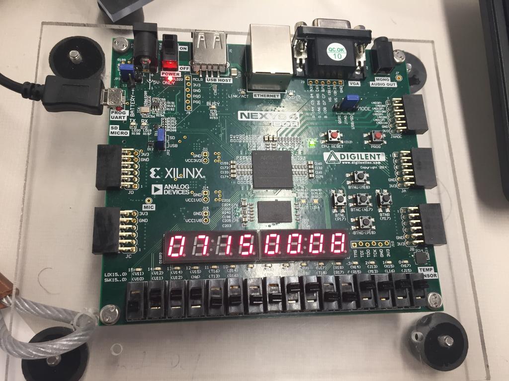
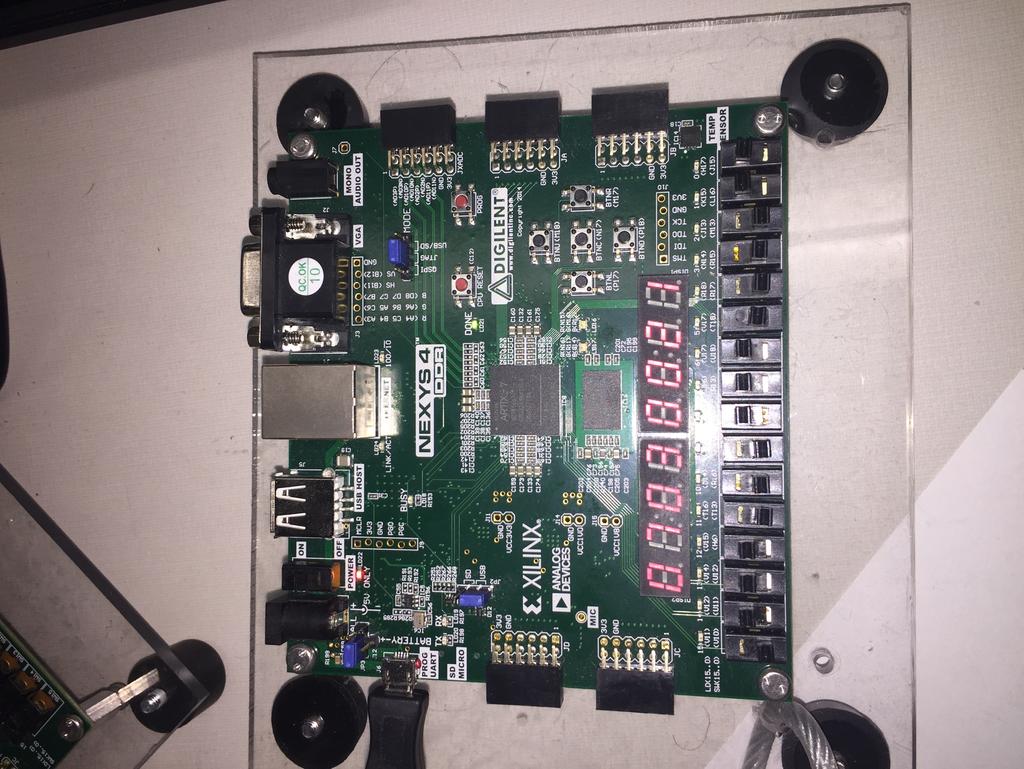
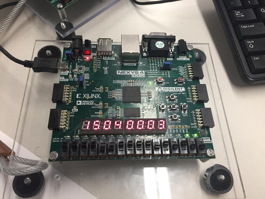
2 Abstract: The purpose of the project was to build a simple calculator using 7seg displays and switches on the Nexys 4 DDR FGPA. The calculator would be able to add, subtract, multiple, and divide 4-bit unsigned numbers. The project was a great learning experience for digital logic and VHDL. An example is interfacing multiple components and performing computations on the FPGA. The project is going to utilize most of the skills learned during the ECE 278 course. Methodology: There will be 2 4-bit unsigned inputs. These inputs will be entered on the bottom of the board using dip switches. The method of operation will be chosen by the user. They will activate 1 of 4 preselected switches. Each switch will correlate with one specific function. Once that switch is pressed that signal will go into a debouncer then a priority encoder. An encoder is used just in case more than one switch is enabled at one time. A 4x1 multiplexer is used to sort Introduction: The scope of the project was building a 4-bit calculator using what we learned in our labs and a FPGA (Nexys 4). The team wanted a project that would involve many topics covered in ECE 278 and challenge the team to complete the project. This was a good project to do because it incorporates many different digital logic principals like architecturally based with arithmetic operations. Some of the topics that were covered in class were Arithmetic Logic Unit (ALU) design, Finite State Machines (FSMs), counters, multiplexers and priority encoders. Topics that will need to be researched outside of class will be how to utilize a debouncer and how to use a serializer. This project has many applications such as being used as a traditional calculator or a part of a larger project that would need calculations performed. out the signals then enter a BCD converter then a 7 segment converted which will be sent to a serializer. The output of the serializer will show on the 7 segment displays. The leftmost 2 displays will show what the input of A is, the next 2 show the value of B. The 4 rightmost display will show the whole number value of the calculation between A and B. If there is a remainder, it will be displayed on 4 LEDs in unsigned binary. The first steps that were taken was to decide what our inputs and outputs would be. After that we then collaborated and designed a top level design that we thought we could successfully implement. After the top level was created we labeled all signals along with their sizes. This is important because in portions of the program input signals must be uniform in order to avoid any errors. This helped us out a lot when
3 making the top level design and port mapping. After that was completed we built each portion of the code. When all errors were taken care of we moved on to the top level then the test bench. We tested out multiple areas to insure everything was working properly before finally implementing the entire project to the FPGA. Top level is shown in Figure (1) Components: Functions: Each function used was created in one of our labs. The division function was modified in order to support 2 4-bit inputs opposed to a 6-bit and 4-bit input. The top levels of each lab are shown on Figures (2,3,4,5). In order to avoid signed values. The subtraction function was created so that the absolute value for the difference between A and B would be taken. It is also worth noting that the quotient of the division function is displayed on the 7 segment display while the remainder is displayed on 4 LEDs. Each LED represent a binary value. The leftmost LED will represent the MSB of a 4-bit binary unsigned value, while the rightmost represents the LSB. Debouncer: The purpose of the debouncer was to insure that when a switch is activated or deactivated there is no fluctuation in the signal. We did this by cascading three delays. A single signal input was entered into the first delay. On the rising edge of the clock the signal will then pass through and enter the second delay. That signal will then pass through the second delay on the next rising edge. The same was done with the third delay. The outputs of each delay were ANDED with each other. This method insures that the signal stays high for three clock ticks before a high output is then passed through the AND gate. The output of the AND gate is the output of the debouncer. If the switch goes low, it only takes one clock tick before the debouncer will output a low signal. We used 4 debouncers, one for each switch which would determine the function that will be performed. See Figure (6) for top level design of debouncer. Priority Encoder: The priority encoder was used to insure that a correct S signal would be sent to both 4x1 multiplexers. Each debouncer output is sent to the encoder. The encoder will then output a 2-bit. This was done by using a when statement. We determined all possible inputs from all four debouncers and gave priority to the MSB which is the division switch, then the multiplication, followed by subtraction then finally addition. If the encoder does not receive a high signal from any debouncer then the encoder sends a signal that will allow the multiplexers to pass through the addition signal. 4x1 Multiplexer: The multiplexers were used to allow only one function output to pass through to the 7 segment displays and LEDS. The first multiplexer would pass through the whole number values of each function which would eventually go to the 7 segment
4 display. The second multiplexer was used to pass through the remainder from the division function to the LEDs. If any other function besides division was chosen, then the second multiplexer would pass through a value of 0 to the LEDs. Binary to BCD Converter: We wanted our calculator to display an output that was in base 10. In order to do this, we had to convert the outputs of our functions to binary converted decimal. This was done by making a table of all possible binary inputs which ranged from which is in decimal. We limited the output to 225 because the max output of the calculator would be 15*15. The we made a table of BCD values with the same range. A when statement was used to tell allow program to choose the correct BCD value based on the binary input. Two different files were created for this, one that could converter only up to 225 and a second that ranged up to This file was made just in case we wanted to increase out input sizes to 6-bits. Ultimately this file was not used because the input size was 4-bits and we didn't want to take up unnecessary memory on the FPGA. BCD to 7 segment Converter: This component was used to send a binary code to the 7 segment display so that the correct BCD value will be displayed. This was again done by making a table and using a when statement. Serializer: This component was needed to allow multiple 7 segment displays to appear as if they are all on at once. A counter was used and set up to interval every 1 millisecond. The counter output was sent to the enable of a finite state machine. The FSM had 8 different states, one state for each 7 segment that we wanted to use. As the counter increases intervals the FSM goes to the next state. Each state would output a unique 3-bit value. This unique signal was then sent to the S input of an 8x1 multiplexer and a 3-to-8 decoder. It would then simultaneously allow one input of the multiplexer to pass through to all 7 segment displays and enable that inputs corresponding display. Even though the multiplexers output is sent to each display, only the one that is enabled will show it. The inputs of the 8x1 multiplexer are A, B and the output of the first 4x1 multiplexer. The displays are flickering once every 8ms for only 1ms. This gives each display the display frequency of 125hz, which is too fast for the human eye to notice. Even though the max output will only need 3 7 segment displays, four were used. This was done just in case we increased the input values of A and B. Results: We were very well prepared for this project. When designing and implementing the program we ran into very few road blocks. One of the roadblocks encountered was displaying multiple values on
5 multiple 7 segment displays at one time. After consulting with our professor we determined that using a serializer was the best option. Another issue faced was making the division to work properly. After troubleshooting we discovered an enable switch would be required in order to allow the FSM in the division function to work properly. Images of the board working are shown in Figure (7). Conclusion: This was a very good learning experience. We had the opportunity to combine multiple files that were made throughout the course along with new ones made specifically for the project. It taught us that planning and hard work in necessary in order to make independent files to come together and work as a function project. There are areas in which we could improve on, such as increasing input size, including signed values and using a keyboard as an interface. Overall we are very happy with what we built together as a team and are grateful he had an opportunity to do this. REFERENCES: Daniel Llamocca ECE 278 Lab 2 F16 [1] Daniel Llamocca ECE 278 Lab 3 F16 [2] Daniel Llamocca ECE 278 Lab 6 F16 [3] Danial Llamocca ECE 378 Midterm Exam W16 [4] Danial Llamocca ECE 278 VHDL Coding for FPGAs Unit 7 Serializer Project F16 [5] Darrin Hannah Lesson 74 Debouncer Circuit [6]

6 Appendix: Figure 1- TopLevel Figure 2 - Addition Toplevel [1] Figure 3 - Subtraction Toplevel [4]
7 Figure 4 - Multiplication Toplevel [2] Figure 5 - Debouncer TopLevel [6] Figure 6 Division Toplevel [3]

8 Figure 6 - Addition Figure 7 - Subtraction
9 Figure 8 - Multiplication Figure 9 - Division
Fixed-Point Calculator
 Fixed-Point Calculator Robert Kozubiak, Muris Zecevic, Cameron Renny Electrical and Computer Engineering Department School of Engineering and Computer Science Oakland University, Rochester, MI rjkozubiak@oakland.edu,
The Calculative Calculator
 The Calculative Calculator Interactive Digital Calculator Chandler Connolly, Sarah Elhage, Matthew Shina, Daniyah Alaswad Electrical and Computer Engineering Department School of Engineering and Computer
Traffic Light Controller. Thomas Quinn, Brandon Londo, Alexander C. Vincent, Yezan Hussein
 Traffic Light Controller Variable Cycle Time Design Thomas Quinn, Brandon Londo, Alexander C. Vincent, Yezan Hussein Electrical and Computer Engineering Department School of Engineering and Computer Science
Traffic Light Controller
 Traffic Light Controller Four Way Intersection Traffic Light System Fall-2017 James Todd, Thierno Barry, Andrew Tamer, Gurashish Grewal Electrical and Computer Engineering Department School of Engineering
Contents Circuits... 1
 Contents Circuits... 1 Categories of Circuits... 1 Description of the operations of circuits... 2 Classification of Combinational Logic... 2 1. Adder... 3 2. Decoder:... 3 Memory Address Decoder... 5 Encoder...
Objectives. Combinational logics Sequential logics Finite state machine Arithmetic circuits Datapath
 Objectives Combinational logics Sequential logics Finite state machine Arithmetic circuits Datapath In the previous chapters we have studied how to develop a specification from a given application, and
Smart Night Light. Figure 1: The state diagram for the FSM of the ALS.
 Smart Night Light Matt Ball, Aidan Faraji-Tajrishi, Thomas Goold, James Wallace Electrical and Computer Engineering Department School of Engineering and Computer Science Oakland University, Rochester,
Combinational Logic Design
 Lab #2 Combinational Logic Design Objective: To introduce the design of some fundamental combinational logic building blocks. Preparation: Read the following experiment and complete the circuits where
ENGG2410: Digital Design Lab 5: Modular Designs and Hierarchy Using VHDL
 ENGG2410: Digital Design Lab 5: Modular Designs and Hierarchy Using VHDL School of Engineering, University of Guelph Fall 2017 1 Objectives: Start Date: Week #7 2017 Report Due Date: Week #8 2017, in the
Ryerson University Department of Electrical and Computer Engineering COE/BME 328 Digital Systems
 1 P a g e Ryerson University Department of Electrical and Computer Engineering COE/BME 328 Digital Systems Lab 6 35 Marks (3 weeks) Design of a Simple General-Purpose Processor Due Date: Week 12 Objective:
EECS 270 Midterm 2 Exam Closed book portion Fall 2014
 EECS 270 Midterm 2 Exam Closed book portion Fall 2014 Name: unique name: Sign the honor code: I have neither given nor received aid on this exam nor observed anyone else doing so. Scores: Page # Points
Introduction to Digital Logic Missouri S&T University CPE 2210 Exam 3 Logistics
 Introduction to Digital Logic Missouri S&T University CPE 2210 Exam 3 Logistics Egemen K. Çetinkaya Egemen K. Çetinkaya Department of Electrical & Computer Engineering Missouri University of Science and
Experiment: FPGA Design with Verilog (Part 4)
") Department of Electrical & Electronic Engineering 2 nd Year Laboratory Experiment: FPGA Design with Verilog (Part 4) 1.0 Putting everything together PART 4 Real-time Audio Signal Processing In this part
Department of Electrical & Electronic Engineering 2 nd Year Laboratory Experiment: FPGA Design with Verilog (Part 4) 1.0 Putting everything together PART 4 Real-time Audio Signal Processing In this part
TSIU03, SYSTEM DESIGN. How to Describe a HW Circuit
 TSIU03 TSIU03, SYSTEM DESIGN How to Describe a HW Circuit Sometimes it is difficult for students to describe a hardware circuit. This document shows how to do it in order to present all the relevant information
Find the equivalent decimal value for the given value Other number system to decimal ( Sample)
") VELAMMAL COLLEGE OF ENGINEERING AND TECHNOLOGY, MADURAI 65 009 Department of Information Technology Model Exam-II-Question bank PART A (Answer for all Questions) (8 X = 6) K CO Marks Find the equivalent
VELAMMAL COLLEGE OF ENGINEERING AND TECHNOLOGY, MADURAI 65 009 Department of Information Technology Model Exam-II-Question bank PART A (Answer for all Questions) (8 X = 6) K CO Marks Find the equivalent
Laboratory 8. Digital Circuits - Counter and LED Display
 Laboratory 8 Digital Circuits - Counter and Display Required Components: 2 1k resistors 1 10M resistor 3 0.1 F capacitor 1 555 timer 1 7490 decade counter 1 7447 BCD to decoder 1 MAN 6910 or LTD-482EC
Decade Counters Mod-5 counter: Decade Counter:
 Decade Counters We can design a decade counter using cascade of mod-5 and mod-2 counters. Mod-2 counter is just a single flip-flop with the two stable states as 0 and 1. Mod-5 counter: A typical mod-5
Electrical and Telecommunications Engineering Technology_TCET3122/TC520. NEW YORK CITY COLLEGE OF TECHNOLOGY The City University of New York
 NEW YORK CITY COLLEGE OF TECHNOLOGY The City University of New York DEPARTMENT: SUBJECT CODE AND TITLE: COURSE DESCRIPTION: REQUIRED: Electrical and Telecommunications Engineering Technology TCET 3122/TC
Microprocessor Design
 Microprocessor Design Principles and Practices With VHDL Enoch O. Hwang Brooks / Cole 2004 To my wife and children Windy, Jonathan and Michelle Contents 1. Designing a Microprocessor... 2 1.1 Overview
Tic-Tac-Toe Using VGA Output Alexander Ivanovic, Shane Mahaffy, Johnathan Hannosh, Luca Wagner
 Tic-Tac-Toe Using VGA Output Alexander Ivanovic, Shane Mahaffy, Johnathan Hannosh, Luca Wagner Electrical and Computer Engineering Department School of Engineering and Computer Science Oakland University,
Vending Machine. Keywords FSM, Vending Machine, FPGA, VHDL
 Vending Machine Khodur Dbouk, Basil Jajou, Kouder Abbas, Stevan Nissan Electrical and Computer Engineering Department School of Engineering and Computer Science Oakland University, Rochester, MI kdbouk@oakland.edu,
Digital Fundamentals: A Systems Approach
 Digital Fundamentals: A Systems Approach Counters Chapter 8 A System: Digital Clock Digital Clock: Counter Logic Diagram Digital Clock: Hours Counter & Decoders Finite State Machines Moore machine: One
Lab 5 FPGA Design Flow Based on Aldec Active-HDL. Fast Reflex Game.
 Lab 5 FPGA Design Flow Based on Aldec Active-HDL. Fast Reflex Game. Task 0 (tested during lab demonstration) Get familiar with the Tutorial on FPGA Design Flow based on Aldec Active-HDL. Be ready to perform
Half-Adders. Ch.5 Summary. Chapter 5. Thomas L. Floyd
 Digital Fundamentals: A Systems Approach Functions of Combinational Logic Chapter 5 Half-Adders Basic rules of binary addition are performed by a half adder, which accepts two binary inputs (A and B) and
EEE130 Digital Electronics I Lecture #1_2. Dr. Shahrel A. Suandi
 EEE130 Digital Electronics I Lecture #1_2 Dr. Shahrel A. Suandi 1-4 Overview of Basic Logic Functions Digital systems are generally built from combinations of NOT, AND and OR logic elements The combinations
Lab #10 Hexadecimal-to-Seven-Segment Decoder, 4-bit Adder-Subtractor and Shift Register. Fall 2017
 University of Texas at El Paso Electrical and Computer Engineering Department EE 2169 Laboratory for Digital Systems Design I Lab #10 Hexadecimal-to-Seven-Segment Decoder, 4-bit Adder-Subtractor and Shift
MODULAR DIGITAL ELECTRONICS TRAINING SYSTEM
 MODULAR DIGITAL ELECTRONICS TRAINING SYSTEM MDETS UCTECH's Modular Digital Electronics Training System is a modular course covering the fundamentals, concepts, theory and applications of digital electronics.
Inside Digital Design Accompany Lab Manual
 1 Inside Digital Design, Accompany Lab Manual Inside Digital Design Accompany Lab Manual Simulation Prototyping Synthesis and Post Synthesis Name- Roll Number- Total/Obtained Marks- Instructor Signature-
DIGITAL SYSTEM DESIGN UNIT I (2 MARKS)
") DIGITAL SYSTEM DESIGN UNIT I (2 MARKS) 1. Convert Binary number (111101100) 2 to Octal equivalent. 2. Convert Binary (1101100010011011) 2 to Hexadecimal equivalent. 3. Simplify the following Boolean function
DIGITAL SYSTEM DESIGN UNIT I (2 MARKS) 1. Convert Binary number (111101100) 2 to Octal equivalent. 2. Convert Binary (1101100010011011) 2 to Hexadecimal equivalent. 3. Simplify the following Boolean function
Course Plan. Course Articulation Matrix: Mapping of Course Outcomes (COs) with Program Outcomes (POs) PSO-1 PSO-2
 with Program Outcomes (POs) PSO-1 PSO-2") Course Plan Semester: 4 - Semester Year: 2019 Course Title: DIGITAL ELECTRONICS Course Code: EC106 Semester End Examination: 70 Continuous Internal Evaluation: 30 Lesson Plan Author: Ms. CH SRIDEVI Last
Course Plan Semester: 4 - Semester Year: 2019 Course Title: DIGITAL ELECTRONICS Course Code: EC106 Semester End Examination: 70 Continuous Internal Evaluation: 30 Lesson Plan Author: Ms. CH SRIDEVI Last
1. Convert the decimal number to binary, octal, and hexadecimal.
 1. Convert the decimal number 435.64 to binary, octal, and hexadecimal. 2. Part A. Convert the circuit below into NAND gates. Insert or remove inverters as necessary. Part B. What is the propagation delay
Digital Electronics II 2016 Imperial College London Page 1 of 8
 Information for Candidates: The following notation is used in this paper: 1. Unless explicitly indicated otherwise, digital circuits are drawn with their inputs on the left and their outputs on the right.
Chapter 8 Functions of Combinational Logic
 ETEC 23 Programmable Logic Devices Chapter 8 Functions of Combinational Logic Shawnee State University Department of Industrial and Engineering Technologies Copyright 27 by Janna B. Gallaher Basic Adders
MASSACHUSETTS INSTITUTE OF TECHNOLOGY Department of Electrical Engineering and Computer Sciences
 MASSACHUSETTS INSTITUTE OF TECHNOLOGY Department of Electrical Engineering and Computer Sciences Introductory Digital Systems Lab (6.111) Quiz #2 - Spring 2003 Prof. Anantha Chandrakasan and Prof. Don
Sequential Logic Design CS 64: Computer Organization and Design Logic Lecture #14
 Sequential Logic Design CS 64: Computer Organization and Design Logic Lecture #14 Ziad Matni Dept. of Computer Science, UCSB Administrative Only 2.5 weeks left!!!!!!!! OMG!!!!! Th. 5/24 Sequential Logic
Introduction to Digital Electronics
 Introduction to Digital Electronics by Agner Fog, 2018-10-15. Contents 1. Number systems... 3 1.1. Decimal, binary, and hexadecimal numbers... 3 1.2. Conversion from another number system to decimal...
1. True/False Questions (10 x 1p each = 10p) (a) I forgot to write down my name and student ID number.
 (a) I forgot to write down my name and student ID number.") CprE 281: Digital Logic Midterm 2: Friday Oct 30, 2015 Student Name: Student ID Number: Lab Section: Mon 9-12(N) Mon 12-3(P) Mon 5-8(R) Tue 11-2(U) (circle one) Tue 2-5(M) Wed 8-11(J) Wed 6-9(Y) Thur 11-2(Q)
CprE 281: Digital Logic Midterm 2: Friday Oct 30, 2015 Student Name: Student ID Number: Lab Section: Mon 9-12(N) Mon 12-3(P) Mon 5-8(R) Tue 11-2(U) (circle one) Tue 2-5(M) Wed 8-11(J) Wed 6-9(Y) Thur 11-2(Q)
ECE Lab 5. MSI Circuits - Four-Bit Adder/Subtractor with Decimal Output
 ECE 201 - Lab 5 MSI Circuits - Four-Bit Adder/Subtractor with Decimal Output PURPOSE To familiarize students with Medium Scale Integration (MSI) technology, specifically adders. The student should also
CS302 Digital Logic Design Solved Objective Midterm Papers For Preparation of Midterm Exam
 CS302 Digital Logic Design Solved Objective Midterm Papers For Preparation of Midterm Exam MIDTERM EXAMINATION Spring 2012 Question No: 1 ( Marks: 1 ) - Please choose one A SOP expression is equal to 1
DIGITAL FUNDAMENTALS
 DIGITAL FUNDAMENTALS A SYSTEMS APPROACH THOMAS L. FLOYD PEARSON Boston Columbus Indianapolis New York San Francisco Upper Saddle River Amsterdam Cape Town Dubai London Madrid Milan Munich Paris Montreal
QUICK GUIDE COMPUTER LOGICAL ORGANIZATION - OVERVIEW
 QUICK GUIDE http://www.tutorialspoint.com/computer_logical_organization/computer_logical_organization_quick_guide.htm COMPUTER LOGICAL ORGANIZATION - OVERVIEW Copyright tutorialspoint.com In the modern
California State University, Bakersfield Computer & Electrical Engineering & Computer Science ECE 3220: Digital Design with VHDL Laboratory 7
 California State University, Bakersfield Computer & Electrical Engineering & Computer Science ECE 322: Digital Design with VHDL Laboratory 7 Rational: The purpose of this lab is to become familiar in using
ET398 LAB 4. Concurrent Statements, Selection and Process
 ET398 LAB 4 Concurrent Statements, Selection and Process Decoders/Multiplexers February 16, 2013 Tiffany Turner OBJECTIVE The objectives of this lab were for us to become more adept at creating VHDL code
Digital Electronic Circuits Design & Laboratory Guideline
 D.2. Encoders Often we use diverse peripheral devices such as switches, numeric keypads and more in order to interface the analog world with the digital one and, along with the usage of these devices,
TYPICAL QUESTIONS & ANSWERS
 DIGITALS ELECTRONICS TYPICAL QUESTIONS & ANSWERS OBJECTIVE TYPE QUESTIONS Each Question carries 2 marks. Choose correct or the best alternative in the following: Q.1 The NAND gate output will be low if
Final Exam review: chapter 4 and 5. Supplement 3 and 4
 Final Exam review: chapter 4 and 5. Supplement 3 and 4 1. A new type of synchronous flip-flop has the following characteristic table. Find the corresponding excitation table with don t cares used as much
BCN1043. By Dr. Mritha Ramalingam. Faculty of Computer Systems & Software Engineering
 BCN1043 By Dr. Mritha Ramalingam Faculty of Computer Systems & Software Engineering mritha@ump.edu.my http://ocw.ump.edu.my/ authors Dr. Mohd Nizam Mohmad Kahar (mnizam@ump.edu.my) Jamaludin Sallim (jamal@ump.edu.my)
Operating Manual Ver.1.1
 Event Counter Operating Manual Ver.1.1 An ISO 9001 : 2000 company 94-101, Electronic Complex Pardesipura, Indore- 452010, India Tel : 91-731- 2570301/02, 4211100 Fax: 91-731- 2555643 e mail : info@scientech.bz
Lab 4: Hex Calculator
 CpE 487 Digital Design Lab Lab 4: Hex Calculator 1. Introduction In this lab, we will program the FPGA on the Nexys2 board to function as a simple hexadecimal calculator capable of adding and subtracting
# "$ $ # %!"$!# &!'$("!)!"! $ # *!"! $ '!!$ #!!)! $ "# ' "
!! $ # *!! $ '!!$ #!!)! $ # '") !" #!""! # "$ $ # %!"$!# &!'$("!)!"! $ # *!"! $ '!!$ #!!)! $ "# ' " % &! # Design a combinational logic circuit 10:4 encoder which has a 10-bit input (D9 to D0) and a 4-bit output. If bit position i of
!" #!""! # "$ $ # %!"$!# &!'$("!)!"! $ # *!"! $ '!!$ #!!)! $ "# ' " % &! # Design a combinational logic circuit 10:4 encoder which has a 10-bit input (D9 to D0) and a 4-bit output. If bit position i of
PHYS 3322 Modern Laboratory Methods I Digital Devices
 PHYS 3322 Modern Laboratory Methods I Digital Devices Purpose This experiment will introduce you to the basic operating principles of digital electronic devices. Background These circuits are called digital
Lab #6: Combinational Circuits Design
 Lab #6: Combinational Circuits Design PURPOSE: The purpose of this laboratory assignment is to investigate the design of combinational circuits using SSI circuits. The combinational circuits being implemented
Dr. Shahram Shirani COE2DI4 Midterm Test #2 Nov 19, 2008
 Page 1 Dr. Shahram Shirani COE2DI4 Midterm Test #2 Nov 19, 2008 Instructions: This examination paper includes 13 pages and 20 multiple-choice questions starting on page 3. You are responsible for ensuring
Sequential Logic Notes
 Sequential Logic Notes Andrew H. Fagg igital logic circuits composed of components such as AN, OR and NOT gates and that do not contain loops are what we refer to as stateless. In other words, the output
COMPUTER ENGINEERING PROGRAM
 COMPUTER ENGINEERING PROGRAM California Polytechnic State University CPE 169 Experiment 6 Introduction to Digital System Design: Combinational Building Blocks Learning Objectives 1. Digital Design To understand
problem maximum score 1 28pts 2 10pts 3 10pts 4 15pts 5 14pts 6 12pts 7 11pts total 100pts
 University of California at Berkeley College of Engineering Department of Electrical Engineering and Computer Sciences EECS150 J. Wawrzynek Spring 2002 4/5/02 Midterm Exam II Name: Solutions ID number:
DEPARTMENT OF COMPUTER SCIENCE & ENGINEERING
 DRONACHARYA GROUP OF INSTITUTIONS, GREATER NOIDA Affiliated to Mahamaya Technical University, Noida Approved by AICTE DEPARTMENT OF COMPUTER SCIENCE & ENGINEERING Lab Manual for Computer Organization Lab
Step 1 - shaft decoder to generate clockwise/anticlockwise signals
 Workshop Two Shaft Position Encoder Introduction Some industrial automation applications require control systems which know the rotational position of a shaft. Similar devices are also used for digital
Logic Devices for Interfacing, The 8085 MPU Lecture 4
 Logic Devices for Interfacing, The 8085 MPU Lecture 4 1 Logic Devices for Interfacing Tri-State devices Buffer Bidirectional Buffer Decoder Encoder D Flip Flop :Latch and Clocked 2 Tri-state Logic Outputs
Serial FIR Filter. A Brief Study in DSP. ECE448 Spring 2011 Tuesday Section 15 points 3/8/2011 GEORGE MASON UNIVERSITY.
 GEORGE MASON UNIVERSITY Serial FIR Filter A Brief Study in DSP ECE448 Spring 2011 Tuesday Section 15 points 3/8/2011 Instructions: Zip all your deliverables into an archive .zip and submit it
Minnesota State College Southeast
 ELEC 2211: Digital Electronics II A. COURSE DESCRIPTION Credits: 4 Lecture Hours/Week: 2 Lab Hours/Week: 4 OJT Hours/Week: *.* Prerequisites: None Corequisites: None MnTC Goals: None Minnesota State College
COE328 Course Outline. Fall 2007
 COE28 Course Outline Fall 2007 1 Objectives This course covers the basics of digital logic circuits and design. Through the basic understanding of Boolean algebra and number systems it introduces the student
WINTER 15 EXAMINATION Model Answer
 Important Instructions to examiners: 1) The answers should be examined by key words and not as word-to-word as given in the model answer scheme. 2) The model answer and the answer written by candidate
Sequential logic circuits
 Computer Mathematics Week 10 Sequential logic circuits College of Information Science and Engineering Ritsumeikan University last week combinational digital circuits signals and busses logic gates and,
Figure 30.1a Timing diagram of the divide by 60 minutes/seconds counter
 Digital Clock The timing diagram figure 30.1a shows the time interval t 6 to t 11 and t 19 to t 21. At time interval t 9 the units counter counts to 1001 (9) which is the terminal count of the 74x160 decade
FPGA Laboratory Assignment 4. Due Date: 06/11/2012
 FPGA Laboratory Assignment 4 Due Date: 06/11/2012 Aim The purpose of this lab is to help you understanding the fundamentals of designing and testing memory-based processing systems. In this lab, you will
Registers and Counters
 Registers and Counters Clocked sequential circuit = F/Fs and combinational gates Register Group of flip-flops (share a common clock and capable of storing one bit of information) Consist of a group of
1. a) For the circuit shown in figure 1.1, draw a truth table showing the output Q for all combinations of inputs A, B and C. [4] Figure 1.
![1. a) For the circuit shown in figure 1.1, draw a truth table showing the output Q for all combinations of inputs A, B and C. [4] Figure 1.](/thumbs/88/117492374.jpg "1. a) For the circuit shown in figure 1.1, draw a truth table showing the output Q for all combinations of inputs A, B and C. [4] Figure 1.") [Question 1 is compulsory] 1. a) For the circuit shown in figure 1.1, draw a truth table showing the output Q for all combinations of inputs A, B and C. Figure 1.1 b) Minimize the following Boolean functions:
[Question 1 is compulsory] 1. a) For the circuit shown in figure 1.1, draw a truth table showing the output Q for all combinations of inputs A, B and C. Figure 1.1 b) Minimize the following Boolean functions:
HDL & High Level Synthesize (EEET 2035) Laboratory II Sequential Circuits with VHDL: DFF, Counter, TFF and Timer
 Laboratory II Sequential Circuits with VHDL: DFF, Counter, TFF and Timer") 1 P a g e HDL & High Level Synthesize (EEET 2035) Laboratory II Sequential Circuits with VHDL: DFF, Counter, TFF and Timer Objectives: Develop the behavioural style VHDL code for D-Flip Flop using gated,
1 P a g e HDL & High Level Synthesize (EEET 2035) Laboratory II Sequential Circuits with VHDL: DFF, Counter, TFF and Timer Objectives: Develop the behavioural style VHDL code for D-Flip Flop using gated,
MODULE 3. Combinational & Sequential logic
 MODULE 3 Combinational & Sequential logic Combinational Logic Introduction Logic circuit may be classified into two categories. Combinational logic circuits 2. Sequential logic circuits A combinational
Laboratory 11. Required Components: Objectives. Introduction. Digital Displays and Logic (modified from lab text by Alciatore)
") Laboratory 11 Digital Displays and Logic (modified from lab text by Alciatore) Required Components: 2x lk resistors 1x 10M resistor 3x 0.1 F capacitor 1x 555 timer 1x 7490 decade counter 1x 7447 BCD to
Laboratory 11 Digital Displays and Logic (modified from lab text by Alciatore) Required Components: 2x lk resistors 1x 10M resistor 3x 0.1 F capacitor 1x 555 timer 1x 7490 decade counter 1x 7447 BCD to
Digital Circuits ECS 371
 Digital Circuits ECS 37 Dr. Prapun Suksompong prapun@siit.tu.ac.th Lecture 0 Office Hours: BKD 360-7 Monday 9:00-0:30, :30-3:30 Tuesday 0:30-:30 Announcement HW4 posted on the course web site Chapter 5:
CprE 281: Digital Logic
 CprE 28: Digital Logic Instructor: Alexander Stoytchev http://www.ece.iastate.edu/~alexs/classes/ Registers and Counters CprE 28: Digital Logic Iowa State University, Ames, IA Copyright Alexander Stoytchev
Registers and Counters
 Registers and Counters Clocked sequential circuit = F/Fs and combinational gates Register Group of flip-flops (share a common clock and capable of storing one bit of information) Consist of a group of
Lab #5: Design Example: Keypad Scanner and Encoder - Part 1 (120 pts)
") Nate Pihlstrom, npihlstr@uccs.edu Lab #5: Design Example: Keypad Scanner and Encoder - Part 1 (120 pts) Objective The objective of lab assignments 5 through 9 are to systematically design and implement
Nate Pihlstrom, npihlstr@uccs.edu Lab #5: Design Example: Keypad Scanner and Encoder - Part 1 (120 pts) Objective The objective of lab assignments 5 through 9 are to systematically design and implement
You will be first asked to demonstrate regular operation with default values. You will be asked to reprogram your time values and continue operation
 Massachusetts Institute of Technology Department of Electrical Engineering and Computer Science 6.111 - Introductory Digital Systems Laboratory (Spring 2006) Laboratory 2 (Traffic Light Controller) Check
ELEC 204 Digital System Design LABORATORY MANUAL
 Elec 24: Digital System Design Laboratory ELEC 24 Digital System Design LABORATORY MANUAL : 4-bit hexadecimal Decoder & 4-bit Increment by N Circuit College of Engineering Koç University Important Note:
Scans and encodes up to a 64-key keyboard. DB 1 DB 2 DB 3 DB 4 DB 5 DB 6 DB 7 V SS. display information.
 Programmable Keyboard/Display Interface - 8279 A programmable keyboard and display interfacing chip. Scans and encodes up to a 64-key keyboard. Controls up to a 16-digit numerical display. Keyboard has
Laboratory Exercise 7
 Laboratory Exercise 7 Finite State Machines This is an exercise in using finite state machines. Part I We wish to implement a finite state machine (FSM) that recognizes two specific sequences of applied
Lesson No Lesson No
 Table of Contents Lesson No. 01 1 An Overview & Number Systems 1 Programmable Logic Devices (PLDs) 8 Fractions in Binary Number System 13 Binary Number System 12 Caveman number system 11 Decimal Number
Chapter 9 MSI Logic Circuits
 Chapter 9 MSI Logic Circuits Chapter 9 Objectives Selected areas covered in this chapter: Analyzing/using decoders & encoders in circuits. Advantages and disadvantages of LEDs and LCDs. Observation/analysis
Theory Lecture Day Topic Practical Day. Week. number systems and their inter-conversion Decimal, Binary. 3rd. 1st. 1st
 Lesson Plan Name of the Faculty : Priyanka Nain Discipline: Electronics & Communication Engg. Semester:5th Subject:DEMP Lesson Plan Duration: 15 Weeks Work Load(Lecture/Practical) per week (In Hours):
EECS 270 Midterm 1 Exam Closed book portion Winter 2017
 EES 270 Midterm 1 Exam losed book portion Winter 2017 Name: unique name: Sign the honor code: I have neither given nor received aid on this exam nor observed anyone else doing so. NOTES: 1. This part of
DALHOUSIE UNIVERSITY Department of Electrical & Computer Engineering Digital Circuits - ECED Experiment 2 - Arithmetic Elements
 DALHOUSIE UNIVERSITY Department of Electrical & Computer Engineering Digital Circuits - ECED 2200 Experiment 2 - Arithmetic Elements Objectives: 1. To implement a Half subtractor circuit 2. To implement
Laboratory Exercise 7
 Laboratory Exercise 7 Finite State Machines This is an exercise in using finite state machines. Part I We wish to implement a finite state machine (FSM) that recognizes two specific sequences of applied
PURBANCHAL UNIVERSITY
 [c] Implement a full adder circuit with a decoder and two OR gates. [4] III SEMESTER FINAL EXAMINATION-2006 Q. [4] [a] What is flip flop? Explain flip flop operating characteristics. [6] [b] Design and
TRAINING KITS ON DIGITAL ELECTRONIC EXPERIMENTS. Verify Truth table for TTL IC s AND, NOT, & NAND GATES
 TRAINING KITS ON DIGITAL ELECTRONIC EXPERIMENTS CEE 2800 Basic Logic Gates using TTL IC's (7 in 1) To verify the truth table For TTL AND, OR. NOT, NAND,NOR, EX-OR, & EX-NOR Gates. Instrument comprises
 UNIT 1 NUMBER SYSTEMS AND DIGITAL LOGIC FAMILIES 1. Briefly explain the stream lined method of converting binary to decimal number with example. 2. Give the Gray code for the binary number (111) 2. 3.
Experiment (6) 2- to 4 Decoder. Figure 8.1 Block Diagram of 2-to-4 Decoder 0 X X
 2- to 4 Decoder. Figure 8.1 Block Diagram of 2-to-4 Decoder 0 X X") 8. Objectives : Experiment (6) Decoders / Encoders To study the basic operation and design of both decoder and encoder circuits. To describe the concept of active low and active-high logic signals. To
8. Objectives : Experiment (6) Decoders / Encoders To study the basic operation and design of both decoder and encoder circuits. To describe the concept of active low and active-high logic signals. To
Advanced Devices. Registers Counters Multiplexers Decoders Adders. CSC258 Lecture Slides Steve Engels, 2006 Slide 1 of 20
 Advanced Devices Using a combination of gates and flip-flops, we can construct more sophisticated logical devices. These devices, while more complex, are still considered fundamental to basic logic design.
Table of Contents Introduction
 Page 1/9 Waveforms 2015 tutorial 3-Jan-18 Table of Contents Introduction Introduction to DAD/NAD and Waveforms 2015... 2 Digital Functions Static I/O... 2 LEDs... 2 Buttons... 2 Switches... 2 Pattern Generator...
R13 SET - 1 '' ''' '' ' '''' Code No: RT21053
 SET - 1 1. a) What are the characteristics of 2 s complement numbers? b) State the purpose of reducing the switching functions to minimal form. c) Define half adder. d) What are the basic operations in
IMPLEMENTATION OF A BINARY SELECTION SYSTEM CREATED IN XILINX USING FPGA
 ANNALS of Faculty Engineering Hunedoara International Journal of Engineering Tome XV [2017] Fascicule 3 [August] ISSN: 1584-2665 [print; online] ISSN: 1584-2673 [CD-Rom; online] a free-access multidisciplinary
CPE 200L LABORATORY 3: SEQUENTIAL LOGIC CIRCUITS UNIVERSITY OF NEVADA, LAS VEGAS GOALS: BACKGROUND: SR FLIP-FLOP/LATCH
 CPE 200L LABORATORY 3: SEUENTIAL LOGIC CIRCUITS DEPARTMENT OF ELECTRICAL AND COMPUTER ENGINEERING UNIVERSITY OF NEVADA, LAS VEGAS GOALS: Learn to use Function Generator and Oscilloscope on the breadboard.
COMP12111: Fundamentals of Computer Engineering
 COMP2: Fundamentals of Computer Engineering Part I Course Overview & Introduction to Logic Paul Nutter Introduction What is this course about? Computer hardware design o not electronics nothing nasty like
Digital Logic. ECE 206, Fall 2001: Lab 1. Learning Objectives. The Logic Simulator
 Learning Objectives ECE 206, : Lab 1 Digital Logic This lab will give you practice in building and analyzing digital logic circuits. You will use a logic simulator to implement circuits and see how they
Lab #12: 4-Bit Arithmetic Logic Unit (ALU)
") Lab #12: 4-Bit Arithmetic Logic Unit (ALU) ECE/COE 0501 Date of Experiment: 4/3/2017 Report Written: 4/5/2017 Submission Date: 4/10/2017 Nicholas Haver nicholas.haver@pitt.edu 1 H a v e r PURPOSE The purpose
Lab #12: 4-Bit Arithmetic Logic Unit (ALU) ECE/COE 0501 Date of Experiment: 4/3/2017 Report Written: 4/5/2017 Submission Date: 4/10/2017 Nicholas Haver nicholas.haver@pitt.edu 1 H a v e r PURPOSE The purpose
CS6201 UNIT I PART-A. Develop or build the following Boolean function with NAND gate F(x,y,z)=(1,2,3,5,7).
=(1,2,3,5,7).") VALLIAMMAI ENGINEERING COLLEGE SRM Nagar, Kattankulathur-603203 DEPARTMENT OF COMPUTER SCIENCE AND ENGINEERING Academic Year: 2015-16 BANK - EVEN SEMESTER UNIT I PART-A 1 Find the octal equivalent of hexadecimal
VALLIAMMAI ENGINEERING COLLEGE SRM Nagar, Kattankulathur-603203 DEPARTMENT OF COMPUTER SCIENCE AND ENGINEERING Academic Year: 2015-16 BANK - EVEN SEMESTER UNIT I PART-A 1 Find the octal equivalent of hexadecimal
SEMESTER ONE EXAMINATIONS 2002
 SEMESTER ONE EXAMINATIONS 2002 EE101 Digital Electronics Solutions Question 1. An assembly line has 3 failsafe sensors and 1 emergency shutdown switch. The Line should keep moving unless any of the following
3/5/2017. A Register Stores a Set of Bits. ECE 120: Introduction to Computing. Add an Input to Control Changing a Register s Bits
 University of Illinois at Urbana-Champaign Dept. of Electrical and Computer Engineering ECE 120: Introduction to Computing Registers A Register Stores a Set of Bits Most of our representations use sets