Deep Silicon Etch Technology for Advanced MEMS Applications
|
|
|
- Geraldine Spencer
- 6 years ago
- Views:
Transcription

1 Deep Silicon Etch Technology for Advanced MEMS Applications Shenjian Liu, Ph.D. Managing Director, AMEC


2 AMEC Company Profile and Product Line-up AMEC HQ, R&D and MF Facility in Shanghai AMEC Taiwan AMEC Singapore AMEC Japan AMEC Korea AMEC USA EUROPE TELTEC Service Center AMEC Product Line-up Dielectric Etch Poly Etch TSV/MEMS Etch MOCVD VOC Entered international market Processed over 24.5M 65-16nm wafers Start to market from advanced etch for Memory Logic applications Entered international market Domestic market share over 50% Entered domestic market 13 systems delivered to customers Entered domestic market Targeting LCD Industry
3 Presentation Outline The Market Trend The Technical Challenges in MEMS Etch AMEC s Strategy and Solutions Summary
4 The Market Trend
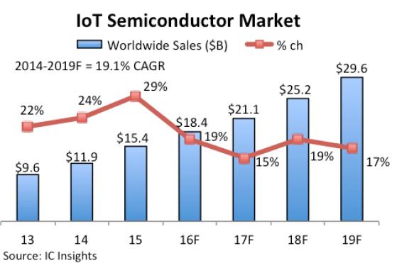
5 MEMS Acceleration


6 Etch Is One of the Critical Process Steps for MEMS Fabrication MEMS AND SENSORS IN MOBILE DEVICES MEMS Etch Example by AMEC Gyrometer Microphone Accelerometer CIS CCD Isolation Source: Yole Development, MSIG Asia, Shanghai, 2016
7 Technical Challenges in MEMS Etch

8 Major Technical Challenges in MEMS Si etch
9 How to Minimize Profile Tilting?


10 Profile Tilting Is One of Major Issues in MEMS Si Etch Si profile tilting affects the resonance frequency of MEMS sensors <0.2 Profile tilting is typically required Vertical Profile Tilt Profile
11 What Is Causing Profile Tilting in MEMS Si Etch? Profile tilting caused by deviation of ion injection angle Two factors influence ion injection angle 1 No uniform plasma Non-uniform Sheath 2 Transition effect at wafer edge Ion injection Bulk plasma Ion inject normal to sheath boundary 2 1 Plasma sheath Wafer
12 Oxide Etch Rate Tilting Angle ( ) Plasma Uniformity Affecting Profile Tilting (5x50 m Si via) Various plasma conditions tested to investigate the effect Less profile tilting with more uniform plasma Plasma uniformity (Oxide Etch Rate uniformity) for various conditions* Experimental Result on Tilting Angle Bad plasma unif Good plasma unif X Position on wafer (mm) Bad plasma unif Good plasma unif X Position (mm) Wafer Titling angle: - 0 +

 Conventional Design")

13 Profile Tilting at Wafer Edge-Sheath Transition Is Critical Profile tilting at wafer edge is improved by optimizing the hardware design at wafer edge Simulation by Dr. Zhou Ning of AMEC Experimental Result (5x50um Si via) Conventional Design with Weak RF Coupling at Wafer Edge Ions Sheath ESC Ceramic Modified Design to Enhance RF Bias Coupling at Wafer Edge Ions Sheath ESC Ceramic Condition: 100 mtorr, 1000sccm Ar, Vdc=204V Wafer Titling angle: - 0 +

14 MEMS Etch Example by AMEC- No Visible Profile Tilting Across Wafer Center Middle Edge 1.5x35 m Trench Etch on 8 Wafer Profile tilting from SEM picture: <0.13 Enabling Technology: Uniform Plasma + Wafer Edge RF Coupling Tuning
15 How to Achieve Smooth Sidewall?

16 Trade Off of Necking and Taper with Non-Bosch Process Lean chemistry: Top Necking Polymerizing Chemistry: Tapered profile Example of Si Via Profile with Non-Bosch Process Ion angle distribution Trade off Deposition Solution: Bosch Process (Cycling of Depo/Etch)


17 Bosch Process Can Easily Form Vertical Profile But with Scallops Why Bosch Process? For Vertical Profile Isotropic etching Deposition Removal of bottom passivation layer by ion bombardment Isotropic etching Resulting profile 10x100 m Si Via


18 Large Scallop Will Lead to Poor Device Performance Major issues of large scallop Inter-via electrical leakage current. Interfacial stress of CVD/ PVD layer Sidewall damage during plasma etch Discontinuous Rough sidewall Smooth sidewall Process flow Nagarajan Ranganathan et al., IEEE TRANSACTIONS ON COMPONENTS, PACKAGING AND MANUFACTURING TECHNOLOGY, 2011 (1), P Sidewall damage during etch Deposition Isotropic Etch Pinhole Poor coverage F Striation


19 Scallops Eliminated by Fast Gas Switching/Shorter Step Time Baseline Step Time Effect on Scallop Size 30% Step time Longer step time Shorter step time Normalized Step Time
 Gas flow Gas flow Sensor Gas Flow Control with MEMS*: Direct sensing the flow Fast response (typically <50msec) * Courtesy of SENSIRION Direct Flow Sensing is Necessary for smooth")
20 Challenge A to Realize Short Step Time- Gas Flow Control Sensor Conventional Gas Flow Control: Sensing gas flow with by-bass sensor Slow response due to indirect sensing (typically >0.5sec) Gas flow Gas flow Sensor Gas Flow Control with MEMS*: Direct sensing the flow Fast response (typically <50msec) * Courtesy of SENSIRION Direct Flow Sensing is Necessary for smooth sidewall


 n SiF 4 F Silicon")
21 10x Faster Gas Switching with MEMS Based Gas Flow Controller Flow Response Comparison* Set point 500sccm Reading Conventional MFC 1sec Set point 500sccm MEMS Based MFC Reading 1sec *Set point: 500sccm C4F8, MFC full scale=500sccm C 4 F 8 SF 6 SiF 4 SF x + SF 6 (CF x ) n SiF 4 F Silicon Silicon Silicon
22 Challenge B to Realize Short Step Time- Step Time Accuracy Step time Step variation Case A: Step time=1sec Variation~0.1sec* (10%) Root causes: Communication delay Step time Step variation Case B: Step time=0.2sec Variation~0.1sec (50%) More accurate time control is needed for shorter step time!

 255ms (actual step time)")
23 Large Variation When Step Time Is Short Example of Step Time Variation 2000ms/div Set Point=200ms Set Point=200ms 500ms/div 453ms (actual step time) 255ms (actual step time) Actual Time= ms
 Total Step time (~900sec) Step time variation Before improvement")
 Total Step time (~900sec) Step time variation With New Communication")
24 Step Time Variation Significantly Reduced with New Technloogy Stress test: 1000cycles(900sec) Total Step time (~900sec) Step time variation Before improvement (Ethernet Based) Time variation: 55.7sec (6%) Total Step time (~900sec) Step time variation With New Communication Technology (Fiber Optics based ) Time variation: 1.5sec (0.17%)


25 Example of Scallop Free TSV Etch (12x100 m) Enabling Technology: Fast Gas Switching + New Communication
26 How to Eliminate Bottom Notch?
soi film stack before Si etching (b) Ion bending due to charge build up on buried oxide layer (c) Notching at SI/oxide interface in a conventional Si etching")
27 Bottom Notching on SOI Caused by Charge Build Up Mask Si Mask Si SiO2 Sub Si Bottom Notching SiO2 Sub Si (a) (b) (c) (a)soi film stack before Si etching (b) Ion bending due to charge build up on buried oxide layer (c) Notching at SI/oxide interface in a conventional Si etching process
28 Bias Pulsing to Reduce Charge-up CW Mode High Power / Low DC* Pulsed Bias Mode Bias ON (DC >=10%) Ion bending Due to charge build up Mask Bias ON Less ion bending due to less charge and high bias Bias Off Charge relaxation due to neutralization Bias ON Less ion bending due to less charge and high bias Si Bottom Notching SiO2 Sub Si ON OFF DC%=ON /(ON+OFF) Charge build-up takes some time Low DC bias pulsing: turn off RF bias before charge builds up

29 Notch Free MEMS Trench Etch Example Very Low DC% Bias Pulsing Needed for Notch Free Profile

30 Stiction Issue with Cavity by Charge-up During Plasma Etch Upper structure Cavity Lower structure Example of Stiction Issue (Gyrometer) Plasma Electrostatic force Stiction Issue Electrons and Ions Hit the wafer and charges build-up during plasma etch Floating structures are common in MEMS device Electrostatic force due to charge-up causes upper and lower structure stuck together Low Duty Cycle Bias Pulsing Required to Minimize Plasma Charge-up
31 CD and Profile Uniformity Control

32 Deposition Rate in Bosch Process is Temperature Sensitive* Deposition Sensitivity= 1.2% / C * Example of Temperature Sensitivity with C 4 F 8 Chemistry by AMEC

33 Example of Tuning ESC Temperature Setting for CD Uniformity Single Zone ESC Temp: Center=Edge=5 C Dual Zone ESC Temp: Center=5 C/Edge= 0 C CD Range= 0.15 m CD Range= 0.03 m

34 Dual zone ESC for CD and profile uniformity control Condition: 3kW RF power from generator; 1.5kW heat goes to ESC Tunable Center hotter Edge hotter Dual Zone Chiller ESC can be used in high RF power applications Better temperature control than using dual zone backside He Better cooling capacity than regular Single Zone ESC Avoids hot spot issues commonly encountered with embedded heaters running high RF power applications


35 Example of Si Trench Etch for Gyroscope Application (2x40 m) Location Center Middle Edge Profile TCD Center/Edge CD Range =0.04 m on Whole Wafer Enabling Technology: Dual Chiller Zone ESC, etc.

36 AMEC s Solution to Challenges in MEMS Etch


37 AMEC TSV/MEMS Etcher Served Available Market MEMS 3D IC LED 2.5D IC Interposer CIS Dicing Not Serve yet Already Served Innovative chamber design to provide solutions to all technical challenges in MEMS and TSV Etch Compact design to deliver high wafer output per footprint with Low COO with dual chamber design

38 Thank You!
Applied Materials. 200mm Tools & Process Capabilities For Next Generation MEMS. Dr Michel (Mike) Rosa
 Rosa") Applied Materials 200mm Tools & Process Capabilities For Next Generation MEMS Dr Michel (Mike) Rosa 200mm MEMS Global Product / Marketing Manager, Components and Systems Group (CSG), Applied Global Services
Applied Materials 200mm Tools & Process Capabilities For Next Generation MEMS Dr Michel (Mike) Rosa 200mm MEMS Global Product / Marketing Manager, Components and Systems Group (CSG), Applied Global Services
Etching Part 2. Saroj Kumar Patra. TFE4180 Semiconductor Manufacturing Technology. Norwegian University of Science and Technology ( NTNU )
") 1 Etching Part 2 Chapter : 16 Semiconductor Manufacturing Technology by M. Quirk & J. Serda Spring Semester 2014 Saroj Kumar Patra, Norwegian University of Science and Technology ( NTNU ) 2 Introduction
1 Etching Part 2 Chapter : 16 Semiconductor Manufacturing Technology by M. Quirk & J. Serda Spring Semester 2014 Saroj Kumar Patra, Norwegian University of Science and Technology ( NTNU ) 2 Introduction
Leveraging 300 mm Technology Solutions to Enable New MEMS Process Capabilities
 Leveraging 300 mm Technology Solutions to Enable New MEMS Process Capabilities Evan Patton Semicon Europa November 2017 Lam Research Corp. 1 Presentation Outline The Internet of Things (IoT) as a market
Sub-micron high aspect ratio silicon beam etch
 Sub-micron high aspect ratio silicon beam etch Gary J. O Brien a,b, David J. Monk b, and Khalil Najafi a a Center for Wireless Integrated Microsystems, Dept. of Electrical Engineering and Computer Science
SINGULATION BY PLASMA ETCHING. INTEGRATION TECHNIQUES TO ENABLE LOW DAMAGE, HIGH PRODUCTIVITY DICING.
 SINGULATION BY PLASMA ETCHING. INTEGRATION TECHNIQUES TO ENABLE LOW DAMAGE, HIGH PRODUCTIVITY DICING. Richard Barnett Dave Thomas Oliver Ansell ABSTRACT Plasma dicing has rapidly gained traction as a viable
Principles of Electrostatic Chucks 6 Rf Chuck Edge Design
 Principles of Electrostatic Chucks 6 Rf Chuck Edge Design Overview This document addresses the following chuck edge design issues: Device yield through system uniformity and particle reduction; System
Reduction of Device Damage During Dry Etching of Advanced MMIC Devices Using Optical Emission Spectroscopy
 Reduction of Device Damage During Dry Etching of Advanced MMIC Devices Using Optical Emission Spectroscopy D. Johnson, R. Westerman, M. DeVre, Y. Lee, J. Sasserath Unaxis USA, Inc. 10050 16 th Street North
Advanced WLP Platform for High-Performance MEMS. Presented by Dean Spicer, Director of Engineering
 Advanced WLP Platform for High-Performance MEMS Presented by Dean Spicer, Director of Engineering 1 May 11 th, 2016 1 Outline 1. Application Drivers for High Performance MEMS Sensors 2. Approaches to Achieving
Overcoming Challenges in 3D NAND Volume Manufacturing
 Overcoming Challenges in 3D NAND Volume Manufacturing Thorsten Lill Vice President, Etch Emerging Technologies and Systems Flash Memory Summit 2017, Santa Clara 2017 Lam Research Corp. Flash Memory Summit
InvenSense Fabless Model for the MEMS Industry
 InvenSense Fabless Model for the MEMS Industry HKSTP Symposium Aug 2016 InvenSense, Inc. Proprietary Outline MEMS Market InvenSense CMOS-MEMS Integration InvenSense Shuttle Program and Process MEMS MARKET
Advanced MEMS Packaging
 Advanced MEMS Packaging John H. Lau Chengkuo Lee C. S. Premachandran Yu Aibin Ш New York Chicago San Francisco Lisbon London Madrid Mexico City Milan New Delhi San Juan Seoul Singapore Sydney Toronto Contents
Abstract. Keywords INTRODUCTION. Electron beam has been increasingly used for defect inspection in IC chip
 Abstract Based on failure analysis data the estimated failure mechanism in capacitor like device structures was simulated on wafer in Front End of Line. In the study the optimal process step for electron
High aspect ratio deep RIE for novel 3D radiation sensors in high energy physics applications
 High aspect ratio deep RIE for novel 3D radiation sensors in high energy physics applications Angela Kok, Thor-Erik Hansen, Trond Hansen, Geir Uri Jensen, Nicolas Lietaer, Michal Mielnik, Preben Storås
HB LEDs & OLEDs. Complete thin film process solutions
 HB LEDs & OLEDs Complete thin film process solutions Get off to a flying start for all your LED thin film deposition and etch processes From 2 inch to 8 inch Manual or fully automated substrate handling
RTNN Etch capabilities
 RTNN Etch capabilities A Partnership Between NC State University, Duke University, and UNC Chapel Hill Trion Minilock II: III-V RIE Trion Phantom II: Oxide/Nitride/Polymer SPTS Pegasus DRIE Trion Minilock
Wafer Thinning and Thru-Silicon Vias
 Wafer Thinning and Thru-Silicon Vias The Path to Wafer Level Packaging jreche@trusi.com Summary A new dry etching technology Atmospheric Downstream Plasma (ADP) Etch Applications to Packaging Wafer Thinning
9 rue Alfred Kastler - BP Nantes Cedex 3 - France Phone : +33 (0) website :
 website :") 9 rue Alfred Kastler - BP 10748-44307 Nantes Cedex 3 - France Phone : +33 (0) 240 180 916 - email : info@systemplus.fr - website : www.systemplus.fr March 2011 - Version 1 Written by: Romain FRAUX DISCLAIMER
9 rue Alfred Kastler - BP 10748-44307 Nantes Cedex 3 - France Phone : +33 (0) 240 180 916 - email : info@systemplus.fr - website : www.systemplus.fr March 2011 - Version 1 Written by: Romain FRAUX DISCLAIMER
Compensation for transient chamber wall condition using realtime plasma density feedback control in an inductively coupled plasma etcher
 Compensation for transient chamber wall condition using realtime plasma density feedback control in an inductively coupled plasma etcher Pete I. Klimecky, J. W. Grizzle, and Fred L. Terry, Jr. Department
GENCOA Key Company Facts. GENCOA is a private limited company (Ltd) Founded 1995 by Dr Dermot Monaghan. Located in Liverpool, UK
 Founded 1995 by Dr Dermot Monaghan. Located in Liverpool, UK") GENCOA Key Company Facts GENCOA is a private limited company (Ltd) Founded 1995 by Dr Dermot Monaghan Located in Liverpool, UK Employs 34 people 6 design (Pro E 3D CAD) 4 process development & simulation
GENCOA Key Company Facts GENCOA is a private limited company (Ltd) Founded 1995 by Dr Dermot Monaghan Located in Liverpool, UK Employs 34 people 6 design (Pro E 3D CAD) 4 process development & simulation
Summary of Selected EMCR650 Projects for Fall 2005 Mike Aquilino Dr. Lynn Fuller
 ROCHESTER INSTITUTE OF TECHNOLOGY MICROELECTRONIC ENGINEERING Summary of Selected EMCR650 Projects for Fall 2005 Mike quilino Dr. Lynn Fuller http://www.rit.edu/~lffeee 82 Lomb Memorial Drive Rochester,
Monolithic Optoelectronic Integration of High- Voltage Power FETs and LEDs
 Monolithic Optoelectronic Integration of High- Voltage Power FETs and LEDs, Zhongda Li, Robert Karlicek and T. Paul Chow Smart Lighting Engineering Research Center Rensselaer Polytechnic Institute, Troy,
Advances in Roll-to-Roll Imprint Lithography for Display Applications Using Self Aligned Imprint Lithography. John G Maltabes HP Labs
 Advances in Roll-to-Roll Imprint Lithography for Display Applications Using Self Aligned Imprint Lithography John G Maltabes HP Labs Outline Introduction Roll to Roll Challenges and Benefits HP Labs Roll
2016, Amkor Technology, Inc.
 1 Standardization of Packaging for the Internet of Things Adrian Arcedera l VP of MEMS and Sensor Products 2 About Amkor Technology Amkor Technology, Inc. is one of the world's largest and most accomplished
Compensation for transient chamber wall condition using real-time plasma density feedback control in an inductively coupled plasma etcher
 Compensation for transient chamber wall condition using real-time plasma density feedback control in an inductively coupled plasma etcher Pete I. Klimecky, a) J. W. Grizzle, and Fred L. Terry, Jr. Department
Because Innovation Matters
 Because Innovation Matters Silicon Systems Group Toru Watanabe President, Applied Materials, Japan Semicon Japan November 30, 2010 Safe Harbor This presentation contains forward-looking statements, including
Plasma dicing 300mm framed wafers - Analysis of improvement in die strength and cost benefits for thin die singulation
 2017 IEEE 67th Electronic Components and Technology Conference Plasma dicing 300mm framed wafers - Analysis of improvement in die strength and cost benefits for thin die singulation Richard Barnett SPTS
Spatial Light Modulators XY Series
 Spatial Light Modulators XY Series Phase and Amplitude 512x512 and 256x256 A spatial light modulator (SLM) is an electrically programmable device that modulates light according to a fixed spatial (pixel)
LEP400 Etch Depth Monitor Real-time, in-situ plasma etch depth monitoring and end point control plus co-linear wafer vision system
 LEP400 Etch Depth Monitor Real-time, in-situ plasma etch depth monitoring and end point control plus co-linear wafer vision system Base Configuration Etch Depth Monitoring LEP400 Recessed Window Plasma
Self-Aligned Double Patterning for 3xnm Flash Production
 Self-Aligned Double Patterning for 3xnm Flash Production Chris Ngai Dir of Process Engineering & Lithography Maydan Technology Center Group Applied Materials, Inc. July 16 th, 2008 Overview Double Patterning
Approaching Zero Etch Bias at Cr Etch Process
 Approaching Zero Etch Bias at Cr Etch Process Pavel Nesladek a ; Norbert Falk b ; Andreas Wiswesser a ; Renee Koch b ; Björn Sass a a Advanced Mask Technology Center, Rähnitzer Allee 9; 01109 Dresden,
Multilevel Beam SOI-MEMS for Optical Applications
 pp. 281-285 Multilevel Beam SOI-MEMS for Optical Applications Veljko Milanović Adriatic Research Institute 2131 University Ave., Suite 322, Berkeley, CA 94704 veljko@adriaticresearch.org Abstract A microfabrication
STMicroelectronics L2G2IS 2-Axis Gyroscope for OIS
 STMicroelectronics L2G2IS 2-Axis Gyroscope for OIS MEMS report by Romain Fraux October 2016 21 rue la Noue Bras de Fer 44200 NANTES - FRANCE +33 2 40 18 09 16 info@systemplus.fr www.systemplus.fr 2016
Fabrication of Lithium Niobate nanopillars using Focused Ion Beam (FIB)
") Fabrication of Lithium Niobate nanopillars using Focused Ion Beam (FIB) Final report for Nanofabrication with Focused Ion and Electron beams course (SK3750) Amin Baghban June 2015 1- Introduction Thanks
Fabrication of Lithium Niobate nanopillars using Focused Ion Beam (FIB) Final report for Nanofabrication with Focused Ion and Electron beams course (SK3750) Amin Baghban June 2015 1- Introduction Thanks
9 rue Alfred Kastler - BP Nantes Cedex 3 - France Phone : +33 (0) website :
 website :") 9 rue Alfred Kastler - BP 10748-44307 Nantes Cedex 3 - France Phone : +33 (0) 240 180 916 - email : info@systemplus.fr - website : www.systemplus.fr January 2012 Written by: Maher SAHMIMI DISCLAIMER :
9 rue Alfred Kastler - BP 10748-44307 Nantes Cedex 3 - France Phone : +33 (0) 240 180 916 - email : info@systemplus.fr - website : www.systemplus.fr January 2012 Written by: Maher SAHMIMI DISCLAIMER :
AIXTRON in EXCILIGHT project
 AIXTRON SE AIXTRON in EXCILIGHT project Gintautas Simkus ABOUT AIXTRON 2 Who we are Headquarter based in Herzogenrath, Germany Worldwide presence with 14 sales/representatives offices and production facilities
Next Generation of Poly-Si TFT Technology: Material Improvements and Novel Device Architectures for System-On-Panel (SOP)
") Next Generation of Poly-Si TFT Technology: Material Improvements and Novel Device Architectures for System-On-Panel (SOP) Tolis Voutsas* Paul Schuele* Bert Crowder* Pooran Joshi* Robert Sposili* Hidayat
Next Generation of Poly-Si TFT Technology: Material Improvements and Novel Device Architectures for System-On-Panel (SOP) Tolis Voutsas* Paul Schuele* Bert Crowder* Pooran Joshi* Robert Sposili* Hidayat
High ResolutionCross Strip Anodes for Photon Counting detectors
 High ResolutionCross Strip Anodes for Photon Counting detectors Oswald H.W. Siegmund, Anton S. Tremsin, Robert Abiad, J. Hull and John V. Vallerga Space Sciences Laboratory University of California Berkeley,
Karl Heinz Feller. Arbeitsgruppe Instrumentelle Analytik FB Medizintechnik und Biotechnologie Ernst-Abbe-Fachhochschule Jena.
 CFD Simulationen von mikrofluidischen Bauelementen zur Optimierung von chemischen Reaktionen Karl Heinz Feller Arbeitsgruppe Instrumentelle Analytik FB Medizintechnik und Biotechnologie Ernst-Abbe-Fachhochschule
2016, Amkor Technology, Inc.
 1 Standardization of Packaging for the Internet of Things Adrian Arcedera l VP of MEMS and Sensor Products 2 About Amkor Technology Amkor Technology, Inc. is one of the world's largest and most accomplished
Pulsed Klystrons for Next Generation Neutron Sources Edward L. Eisen - CPI, Inc. Palo Alto, CA, USA
 Pulsed Klystrons for Next Generation Neutron Sources Edward L. Eisen - CPI, Inc. Palo Alto, CA, USA Abstract The U.S. Department of Energy (DOE) Office of Science has funded the construction of a new accelerator-based
1. Publishable summary
 1. Publishable summary 1.1. Project objectives. The target of the project is to develop a highly reliable high brightness conformable low cost scalable display for demanding applications such as their
EE C247B ME C218 Introduction to MEMS Design Spring 2017
 EE C247B ME C218 Introduction to MEMS Design Spring 2017 Prof. Clark T.-C. Nguyen Dept. of Electrical Engineering & Computer Sciences University of California at Berkeley Berkeley, CA 94720 Lecture Module
CMP and Current Trends Related to Advanced Packaging
 CMP and Current Trends Related to Advanced Packaging Robert L. Rhoades, Ph.D. NCCAVS TFUG-CMPUG Joint Meeting June 7, 2017 Semiconductor Equipment Spare Parts and Service CMP Foundry Foundry Click to edit
Pressure sensor. Surface Micromachining. Residual stress gradients. Class of clean rooms. Clean Room. Surface micromachining
 Pressure sensor Surface Micromachining Deposit sacrificial layer Si PSG By HF Poly by XeF2 Pattern anchors Deposit/pattern structural layer Etch sacrificial layer Surface micromachining Structure sacrificial
Vesper VM1000 Piezoelectric MEMS Microphone
 Vesper VM1000 Piezoelectric MEMS Microphone MEMS report by Sylvain Hallereau February 2017 21 rue la Noue Bras de Fer 44200 NANTES - FRANCE +33 2 40 18 09 16 info@systemplus.fr www.systemplus.fr 2017 System
SEMICONDUCTOR TECHNOLOGY -CMOS-
 SEMICONDUCTOR TECHNOLOGY -CMOS- Fire Tom Wada What is semiconductor and LSIs Huge number of transistors can be integrated in a small Si chip. The size of the chip is roughly the size of nails. Currently,
Selective isotropic etching of Group IV semiconductors to enable gate all around device architectures
 TEL Technology Center, America, LLC - imec Selective isotropic etching of Group IV semiconductors to enable gate all around device architectures SPCC, April 10, 2018 S. Kal 1, C. Pereira 1, Y. Oniki 2,
The PHI VersaProbe operates with two essential software programs: PHI Summitt and Vacuum Watcher. A third program, MultiPak, handles data reduction.
 PHI VersaProbe Scanning XPS System I. Overview The PHI VersaProbe operates with two essential software programs: PHI Summitt and Vacuum Watcher. A third program, MultiPak, handles data reduction. PHI Summitt
SPATIAL LIGHT MODULATORS
 SPATIAL LIGHT MODULATORS Reflective XY Series Phase and Amplitude 512x512 A spatial light modulator (SLM) is an electrically programmable device that modulates light according to a fixed spatial (pixel)
Single-Step CMOS Compatible Fabrication of High Aspect Ratio Microchannels Embedded in Silicon
 Delft University of Technology Single-Step CMOS Compatible Fabrication of High Aspect Ratio Microchannels Embedded in Silicon Kluba, Marta; Arslan, Aslihan; Stoute, Ronald; Muganda, James; Dekker, Ronald
The PEFP 20-MeV Proton Linear Accelerator
 Journal of the Korean Physical Society, Vol. 52, No. 3, March 2008, pp. 721726 Review Articles The PEFP 20-MeV Proton Linear Accelerator Y. S. Cho, H. J. Kwon, J. H. Jang, H. S. Kim, K. T. Seol, D. I.
MAXIM INTEGRATED PRODUCTS
 RELIABILITY REPORT FOR MAX3612ETM+T PLASTIC ENCAPSULATED DEVICES December 22, 2011 MAXIM INTEGRATED PRODUCTS 120 SAN GABRIEL DR. SUNNYVALE, CA 94086 Approved by Richard Aburano Quality Assurance Manager,
2-Axis Gyroscopes for Optical Image Stabilization: STMicroelectronics L2G2IS and InvenSense IDG-2030
 2-Axis Gyroscopes for Optical Image Stabilization: STMicroelectronics L2G2IS and InvenSense IDG-2030 Complete reports and comparison of the latest generation products for smartphones from the leading optical
SEMICONDUCTOR TECHNOLOGY -CMOS-
 SEMICONDUCTOR TECHNOLOGY -CMOS- Fire Tom Wada 2011/12/19 1 What is semiconductor and LSIs Huge number of transistors can be integrated in a small Si chip. The size of the chip is roughly the size of nails.
ksa ScanningPyro ksa ScanningPyro Full Carrier Temperature Maps at the Click of a Button!
 ksa ScanningPyro Full Carrier Temperature Maps at the Click of a Button! The ksa ScanningPyro metrology tool is designed to quickly, easily, and accurately generate full wafer carrier temperature maps
High Performance Microprocessor Design and Automation: Overview, Challenges and Opportunities IBM Corporation
 High Performance Microprocessor Design and Automation: Overview, Challenges and Opportunities Introduction About Myself What to expect out of this lecture Understand the current trend in the IC Design
3D-CHIP TECHNOLOGY AND APPLICATIONS OF MINIATURIZATION
 3D-CHIP TECHNOLOGY AND APPLICATIONS OF MINIATURIZATION 23.08.2018 I DAVID ARUTINOV CONTENT INTRODUCTION TRENDS AND ISSUES OF MODERN IC s 3D INTEGRATION TECHNOLOGY CURRENT STATE OF 3D INTEGRATION SUMMARY
vacuum analysis surface science plasma diagnostics gas analysis
 Hiden ESPION series electrostatic plasma probes Advanced Langmuir probes for plasma diagnostics vacuum analysis surface science plasma diagnostics gas analysis versatility ESPION from Hiden Analytical
RF Solutions for Science.
 RF Solutions for Science www.thalesgroup.com State-of-the-art RF sources for your scientific needs High-power klystrons HIGH KLYSTRONS WITH RF LONG PULSE above 50 μs Thales has been one of the leading
Introduction to. Micragem: A Silicon-on-Insulator Based Micromachining Process. Report ICI-138 V3.0 (Beta version)
") Introduction to Micragem: A Silicon-on-Insulator Based Micromachining Process Report ICI-138 V3.0 (Beta version) December 14, 2004 Copyright 2004 Canadian Microelectronics Corporation This document was
Introduction to Micragem: A Silicon-on-Insulator Based Micromachining Process Report ICI-138 V3.0 (Beta version) December 14, 2004 Copyright 2004 Canadian Microelectronics Corporation This document was
MAXIM INTEGRATED PRODUCTS
 RELIABILITY REPORT FOR PLASTIC ENCAPSULATED DEVICES May 4, 2009 MAXIM INTEGRATED PRODUCTS 120 SAN GABRIEL DR. SUNNYVALE, CA 94086 Approved by Ken Wendel Quality Assurance Director, Reliability Engineering
Standard Operating Manual
 Standard Operating Manual LAM490 AutoEtch System Copyright 11.2015 by Hong Kong University of Science & Technology. All rights reserved. Page 1 Contents 1. Picture and Location 2. Process Capabilities
Nano-Imprint Lithography Infrastructure: Imprint Templates
 Nano-Imprint Lithography Infrastructure: Imprint Templates John Maltabes Photronics, Inc Austin, TX 1 Questions to keep in mind Imprint template manufacturability Resolution Can you get sub30nm images?
MAXIM INTEGRATED PRODUCTS
 RELIABILITY REPORT FOR MAX3639ETM+ PLASTIC ENCAPSULATED DEVICES June 21, 2010 MAXIM INTEGRATED PRODUCTS 120 SAN GABRIEL DR. SUNNYVALE, CA 94086 Approved by Richard Aburano Quality Assurance Manager, Reliability
Lecture 20 Optical MEMS (2)
") EEL6935 Advanced MEMS (Spring 2005) Instructor: Dr. Huikai Xie Lecture 20 Optical MEMS (2) Agenda: MOEMS Introduction Micromirrors EEL6935 Advanced MEMS 2005 H. Xie 3/30/2005 1 Optical MEMS Topics Introduction
EEL6935 Advanced MEMS (Spring 2005) Instructor: Dr. Huikai Xie Lecture 20 Optical MEMS (2) Agenda: MOEMS Introduction Micromirrors EEL6935 Advanced MEMS 2005 H. Xie 3/30/2005 1 Optical MEMS Topics Introduction
State of the art RF generators
 State of the art RF generators cost-efficient adaptation to your systems Speaker: Andreea Vasiliu Business Manager Speaker: Tobias Keller Productmanager RFsystems 1 About SPM SPM is a private and independent
FAST, MEMS-BASED, PHASE-SHIFTING INTERFEROMETER 1
 FAST, MEMS-BASED, PHASE-SHIFTING INTERFEROMETER 1 Hyuck Choo 2, Rishi Kant 3, David Garmire 2, James Demmel 2, and Richard S. Muller 2 2 Berkeley Sensor & Actuator Center, University of California, Berkeley,
EQUIPMENT COATING SYSTEMS FOR THIN-FILM PV THIN-FILM PHOTOVOLTAICS. SCALA VISS PIA nova GC120VCR XENIA
 THIN-FILM PHOTOVOLTAICS EQUIPMENT COATING SYSTEMS FOR THIN-FILM PV SCALA VISS PIA nova GC120VCR XENIA OUR STORY. OUR EXPERIENCE. RANGE OF APPLICATIONS VON ARDENNE provides advanced PVD coating equipment
Micromachining Technology for Lateral Field Emission Devices
 166 IEEE TRANSACTIONS ON ELECTRON DEVICES, VOL. 48, NO. 1, JANUARY 2001 Micromachining Technology for Lateral Field Emission Devices Veljko Milanović, Member, IEEE, Lance Doherty, Student Member, IEEE,
Semiconductors Displays Semiconductor Manufacturing and Inspection Equipment Scientific Instruments
 Semiconductors Displays Semiconductor Manufacturing and Inspection Equipment Scientific Instruments Electronics 110-nm CMOS ASIC HDL4P Series with High-speed I/O Interfaces Hitachi has released the high-performance
Optimizing BNC PCB Footprint Designs for Digital Video Equipment
 Optimizing BNC PCB Footprint Designs for Digital Video Equipment By Tsun-kit Chin Applications Engineer, Member of Technical Staff National Semiconductor Corp. Introduction An increasing number of video
Scalable self-aligned active matrix IGZO TFT backplane technology and its use in flexible semi-transparent image sensors. Albert van Breemen
 Scalable self-aligned active matrix IGZO TFT backplane technology and its use in flexible semi-transparent image sensors Albert van Breemen Image sensors today 1 Dominated by silicon based technology on
Development of high power gyrotron and EC technologies for ITER
 1 Development of high power gyrotron and EC technologies for ITER K. Sakamoto 1), K.Kajiwara 1), K. Takahashi 1), Y.Oda 1), A. Kasugai 1), N. Kobayashi 1), M.Henderson 2), C.Darbos 2) 1) Japan Atomic Energy
ET-5050x-BF1W Datasheet
 PLCC Series ET-5050x-BF1W Datasheet Features : High luminous Intensity and high efficiency Based on GaN technology Wide viewing angle : 120 Excellent performance and visibility Suitable for all SMT assembly
Beam Loss Detection for MPS at FRIB
 Beam Loss Detection for MPS at FRIB Zhengzheng Liu Beam Diagnostics Physicist This material is based upon work supported by the U.S. Department of Energy Office of Science under Cooperative Agreement DE-SC0000661.
Research & Development of Surface-Discharge Color Plasma Display Technologies. Tsutae Shinoda
 esearch & Development of Surface-Discharge Color Plasma Display Technologies Tsutae Shinoda Peripheral System Laboratories,Fujitsu Laboratories Ltd. 64, Nishiwaki, Ohkubo-cho, Akashi 674-8555 Japan Abstract
Sharif University of Technology. SoC: Introduction
 SoC Design Lecture 1: Introduction Shaahin Hessabi Department of Computer Engineering System-on-Chip System: a set of related parts that act as a whole to achieve a given goal. A system is a set of interacting
FinFETs & SRAM Design
 FinFETs & SRAM Design Raymond Leung VP Engineering, Embedded Memories April 19, 2013 Synopsys 2013 1 Agenda FinFET the Device SRAM Design with FinFETs Reliability in FinFETs Summary Synopsys 2013 2 How
Durham Magneto Optics Ltd. NanoMOKE 3 Wafer Mapper. Specifications
 Durham Magneto Optics Ltd NanoMOKE 3 Wafer Mapper Specifications Overview The NanoMOKE 3 Wafer Mapper is an ultrahigh sensitivity Kerr effect magnetometer specially configured for measuring magnetic hysteresis
SLAC R&D Program for a Polarized RF Gun
 ILC @ SLAC R&D Program for a Polarized RF Gun SLAC-PUB-11657 January 2006 (A) J. E. CLENDENIN, A. BRACHMANN, D. H. DOWELL, E. L. GARWIN, K. IOAKEIMIDI, R. E. KIRBY, T. MARUYAMA, R. A. MILLER, C. Y. PRESCOTT,
OLED ON CMOS: WHAT ABOUT THINNING AND BENDING?
 Large cost-effective OLED microdisplays and their applications OLED ON CMOS: WHAT ABOUT THINNING AND BENDING? IDW2017 tony.maindron@cea.fr T. Maindron, B. Chambion, A. Vandeneynde, S. Gétin, M. Provost,
Challenges for OLED Deposition by Vacuum Thermal Evaporation. D. W. Gotthold, M. O Steen, W. Luhman, S. Priddy, C. Counts, C.
 Challenges for OLED Deposition by Vacuum Thermal Evaporation D. W. Gotthold, M. O Steen, W. Luhman, S. Priddy, C. Counts, C. Roth June 7, 2011 Outline Introduction to Veeco Methods of OLED Deposition Cost
FLEX2017 June, Monterey, USA Dr Mike Cowin, CMO, SmartKem.
 FLEX2017 June, Monterey, USA Dr Mike Cowin, CMO, SmartKem. FLEX2017 June, Monterey, USA Dr Mike Cowin, CMO, SmartKem. EU H2020 FLEXTRANs Grant Objectives A 24 month project (started September 2016) (Grant
Advanced Display Manufacturing Technology
 Advanced Display Manufacturing Technology John Busch Vice President, New Business Development Display and Flexible Technology Group September 28, 2017 Safe Harbor This presentation contains forward-looking
Screen investigations for low energetic electron beams at PITZ
 1 Screen investigations for low energetic electron beams at PITZ S. Rimjaem, J. Bähr, H.J. Grabosch, M. Groß Contents Review of PITZ setup Screens and beam profile monitors at PITZ Test results Summary
Flexible Electronics Production Deployment on FPD Standards: Plastic Displays & Integrated Circuits. Stanislav Loboda R&D engineer
 Flexible Electronics Production Deployment on FPD Standards: Plastic Displays & Integrated Circuits Stanislav Loboda R&D engineer The world-first small-volume contract manufacturing for plastic TFT-arrays
13th MOST Interconnectivity Conference 2012 MOST150 on the Road with Avago FOTs
 13th MOST Interconnectivity Conference 2012 MOST150 on the Road with Avago FOTs Thomas Lichtenegger Nov, 15 th 2012 Agenda Avago Avago Fiberoptics MOST150 Development Performance Characterization Quality
I. Introduction. II. Problem
 Wiring Deformable Mirrors for Curvature Adaptive Optics Systems Joshua Shiode Boston University, IfA REU 2005 Sarah Cook University of Hawaii, IfA REU 2005 Mentor: Christ Ftaclas Institute for Astronomy,
Project TRIPLE-S Microscope: Contribution of AMG Technology Ltd.
 Project TRIPLE-S Microscope: Contribution of AMG Technology Ltd. V. Stavrov, G. Stavreva EUROSTARS ROADSHOW - SOFIA, May 26 th, 2015 1 About AMG Technology Ltd. Company Technology background Project TRIPLE-S
MPI Cable Selection Guide
 MPI Cable Selection Guide MPI engineers focus to provide on optimal cable solutions taking into account a number of requirements specific for wafer-level measurement systems: optimal cable length, cable
Structure, Process & Cost Analysis
 Reverse Costing Structure, Process & Cost Analysis Heimann Sensor 32 x 32-array thermopile LWIR image sensor with silicon lens A small, easy to use, low-power, cheap non-contact temperature measurement
MAXIM INTEGRATED PRODUCTS
 RELIABILITY REPORT FOR EEE+ PLASTIC ENCAPSULATED DEVICES February 18, 2010 MAXIM INTEGRATED PRODUCTS 120 SAN GABRIEL DR. SUNNYVALE, CA 94086 Approved by Ken Wendel Quality Assurance Director, Reliability
Discrete Mode Laser Diodes emitting at l~689 and 780nm for Optical Atomic clock applications.
 Discrete Mode Laser Diodes emitting at l~689 and 780nm for Optical Atomic clock applications. Richard Phelan*, M. Gleeson, J. O'Carroll, D. Byrne, L. Maigyte, R. Lennox, K. Carney. J. Somers and B.Kelly
SE-SMD0603-PW65 SMD 0603 purweiss, wasserklar
 1. Features: Lighting Color: Ultra Bright Pure White Lens Color: Water Clear Flat Mold 2. (Package Dimensions): Notes: All dimensions are in millimeters. Tolerance is ± 0.10mm unless otherwise noted 03.05.2017
Technology Overview LTCC
 Sheet Code RFi0604 Technology Overview LTCC Low Temperature Co-fired Ceramic (LTCC) is a multilayer ceramic substrate technology that allows the realisation of multiple embedded passive components (Rs,
2 Work Package and Work Unit descriptions. 2.8 WP8: RF Systems (R. Ruber, Uppsala)
") 2 Work Package and Work Unit descriptions 2.8 WP8: RF Systems (R. Ruber, Uppsala) The RF systems work package (WP) addresses the design and development of the RF power generation, control and distribution
2 Work Package and Work Unit descriptions 2.8 WP8: RF Systems (R. Ruber, Uppsala) The RF systems work package (WP) addresses the design and development of the RF power generation, control and distribution
Dynamic IR Scene Projector Based Upon the Digital Micromirror Device
 Dynamic IR Scene Projector Based Upon the Digital Micromirror Device D. Brett Beasley, Matt Bender, Jay Crosby, Tim Messer, and Daniel A. Saylor Optical Sciences Corporation www.opticalsciences.com P.O.
Commissioning the TAMUTRAP RFQ cooler/buncher. E. Bennett, R. Burch, B. Fenker, M. Mehlman, D. Melconian, and P.D. Shidling
 Commissioning the TAMUTRAP RFQ cooler/buncher E. Bennett, R. Burch, B. Fenker, M. Mehlman, D. Melconian, and P.D. Shidling In order to efficiently load ions into a Penning trap, the ion beam should be
Defense Technical Information Center Compilation Part Notice
 UNCLASSIFIED Defense Technical Information Center Compilation Part Notice ADPO1 1322 TITLE: Amorphous- Silicon Thin-Film Transistor With Two-Step Exposure Process DISTRIBUTION: Approved for public release,
Mechanical aspects, FEA validation and geometry optimization
 RF Fingers for the new ESRF-EBS EBS storage ring The ESRF-EBS storage ring features new vacuum chamber profiles with reduced aperture. RF fingers are a key component to ensure good vacuum conditions and