2016, Amkor Technology, Inc.
|
|
|
- Nathan Cox
- 6 years ago
- Views:
Transcription
1 1
2 Standardization of Packaging for the Internet of Things Adrian Arcedera l VP of MEMS and Sensor Products 2
3 About Amkor Technology Amkor Technology, Inc. is one of the world's largest and most accomplished providers of state-of-the-art packaging design, assembly and test services. Founded in 1968, Amkor is a strategic partner to leading semiconductor companies and electronics OEMs. Our operational base encompasses over 5.8M ft 2 of volume production, development, sales and support services in Asia, Europe and the US. Our solutions enable our customers to focus on semiconductor design and wafer fabrication while utilizing Amkor as their turnkey provider and, where required, their packaging technology innovator. 3
 2018 $57.")

4 The Internet of Things IC Insights ($96B) 2018 $57.6B Value Segmentation Services 60% $15.4B Hardware 16% $11.5B Software 12% $11.5B 12% Semiconductors 4


5 The Building Blocks of the Internet of Things Internet of Things 5

6 General IoT Packaging Requirements Low cost Low power RF requirements (shielding) Scalable to high volume manufacturing Small package size Discrete solution Integrated solution Stimulus delivery 6


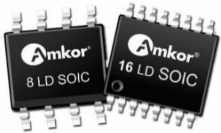
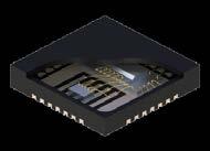
7 Current Discrete Packaging for IoT Connectivity Memory Power Management Microprocessor & Microcontroller MEMS & Sensor SOIC/TSSOP * QFN/TQFP * Laminate CSP * WLCSP * Note: *Limited Compatibility 7
8 What makes MEMS and Sensor Packaging Different? 8


9 Growth and Adoption of Automotive MEMS Sensors The role of government regulations in the MEMS market Fuel Economy Improvements Airbags Tire Pressure Monitoring Electronic Stability Control Pedestrian/ Collision Avoidance? 1970 s 1980 s 1990 s 2000 s 2010 s 2020 s 9


10 Rapid Growth in Consumer MEMS Color Inkjet iphone iphone 4 Samsung S4/iPhone 5S Wearables Nintendo Wii iphone 3GS Samsung S3 Samsung S5 <


11 The Packaging Challenge Stimulus Delivery MEMS are NOT ICs! MEMS Micro Electro Mechanical Systems are tiny structures created in the silicon designed to respond to various stimuli from the real world Source: Yole 2014 MEMS Industry Report No standard process (CMOS, BiCMOS ) No p-n junction for MEMS And as a consequence, NO ROADMAP Bell Labs, US nm Technology Sandia s, Micromachine (MEMS) Courtesy Sandia National Laboratories SUMMiT Technologies 11
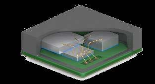
12 MEMS and Sensor Packaging Requirements Accel/Gyro Magnetic Microphone Wafer Capped Wafer Handling Handling Stealth Dicing Stimulus Package Port Hole (Top) Delivery Package Port Hole (Bottom) Low Modulus DA Thermal DA Low CTE Substrates Die Attach Multi Die-Stacked Options Multi Die-SBS FlipStack Multi Sensor Wirebond Au Stud Bump Interconnect Flip Chip Options TSV* Copper Pillar + COW *TSV, TGV is at foundry level. Temperature/ Humidity Pressure/ Altimeter Gas Gesture IR RF/BAW/Saw/ Oscillator Bio/Med 12
13 MEMS and Sensor Packaging Requirements Package Protection Cavity Fill/ Die Coat Accel/Gyro Magnetic Microphone Temperature/ Humidity Overmolded Leadframe Overmolded Laminate Lidded Package Lidded + Molded Package Bio-compatible Lid Exposed Die Non-Ferromagnetic Port Hole Filter EMI Shielding Black Die Coating Clear Die Mold Gel Fill Pressure/ Altimeter Gas Gesture IR RF/BAW/Saw/ Oscillator Bio/Med 13

14 MEMS Capping/Interconnect Trend MEMS Wafer Capping Inter-connection Packaging Bare Die Hermetic Packaging MEMS Device Silicon Cap Glass Cap Thin Film Capping (RnD Stage) 3D Functional Cap Through Silicon Vias Through Glass Vias Cavity Packaging Overmolded CSP/MLF Pre-Mold/Cavity TBD Overmolded CSP Cavity CSP Chip on Chip WLCSP *TSV, TGV is at foundry level. 14


15 MEMS Packaging Complexity Wire type, loop radius and gauge? Molded-in stress? Leaded or not? Overmolded or cavity package? Wirebond or flip-chip? Stacked die or side-by-side? EMI shielding? Encapsulation? Die attach material? Laminate or leadframe? How/what to test? 15

16 Materials Help Manage Die Stress Modulus - MPa Die Attach Adhesives Epoxy - C Film Epoxy - NC Silicone1 Silicone2 S1 Principal Stress - MPa Substrate Thickness/Material Thin Thick FR5 Ceramic FR5-1 FR5-2 From material datasheets From simulation results 16


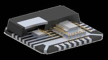
17 Packaging Technologies and Material Sets are the Performance Differentiator Vertical Height Series1 Series2 Series
18 MEMS/Sensor Package Standardization 19


19 Standard Platforms Enable Faster Development for MEMS/Sensor Discrete Packaging 20

20 Evolution Towards Standardization for MEMS/Sensor Packaging Overmolded Exposed Die Surface Cavity Package SOIC QFN Laminate LGA/FPBGA 21


21 Cost vs. Performance Comparison Low Package Cost Ceramic Package High Overmolded Exposed Die Pre-Mold & Cavity High Die Top Stress Low 22
22 Market Acceptance SOIC QFN Laminate LGA/FPBGA Overmolded Exposed Die Surface Widely accepted in the automotive market Cavity package used in automotive pressure sensors Cavity Package Smaller footprint than SOIC, well suited for consumer market Available wettable flank enables more automotive applications Small size and design flexibility make it favorable for sensor fusion and IoT applications for the consumer market Laminate + cavity package provides very good flexibility Gaining traction in automotive markets 23

23 Today s Sensor Clusters 24


24 Sensor Fusion Trend MEMS Wafer Capping Inter-connection Packaging MEMS Sensors Capped, Uncapped Sensors 3D Functional Cap Flip Chip, Stacked Wirebond, Side by Side, Stacked Through Silicon Vias Chip on Chip Overmolded CSP Cavity Packaging Overmolded CSP Cavity CSP WLCSP *TSV, TGV is at foundry level. 25

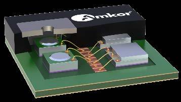
25 Adding IoT Blocks to MEMS/Sensor Package Connectivity Bluetooth Radio LGA Package Pkg Size ~ 3mm sq MEMS/Sensor Inertial Sensor LGA Package Pkg Size ~ 3.5 mm sq IOT Package 8-bit Microcontroller LGA Package Pkg Size ~ 5 mm sq Microcontroller LGA Package Pkg Size ~ 6 mm sq 26


26 Adding IoT Blocks to MEMS/Sensor Package Cavity Package Hybrid Cavity Package MLF /QFN Laminate LGA/FPBGA 27
27 Discrete vs. Integrated IoT Solutions Prospects Integrated Smaller body size, smaller motherboard space Packaging cost reduction Less complex SMT process Less inventory (for IoT blocks) Potential Concerns Known good IoT block/components MEMS/Sensor die stress management Compounded yield, multi test and sensor trimming Prospects Discrete Widely available, existing assembly and test infrastructure Flexible sources of IoT blocks/components Known good IoT block/component binning Potential Concerns Larger motherboard space Limited package size reduction 28
28 In Summary Integration is happening at the front-end to complete the building blocks of IoT The discrete packaging solutions are available today, but Integration and the IoT module assembly is needed to push IoT into more applications MEMS/Sensor device packaging standardization can be applied to IoT module assembly to offer a single package solution without sacrificing performance Standard IoT platforms = faster development Faster introduction of new products IoT monetization 29


29 What will you integrate? Connectivity Power Management + Memory + Microprocessor/ Microcontrollers + MEMS/ Sensors = = IoT 30

30 Next Steps to Standard Packaging and Test Standard package platforms will help speed up integration and monetize IoT What will you integrate? Standard Packaging for IoT What are the priority MEMS / Sensor devices? Will it be MEMS + Connectivity or MEMS + Microcontroller + Connectivity? Etc. Standard Pre-mold Package Outlines? Special features needed - Antenna? Shielding? Tester and Handler Development How can we minimize Test time and reduce the number of insertion? 31

31 Thank You 32

32 Contact Amkor for Further Information San Jose Sales Office 25 Metro Drive Suite 700 San Jose, CA USA Corporate Headquarters 2045 East Innovation Circle Tempe, AZ USA Tel: Tel:


33 Q & A 34
2016, Amkor Technology, Inc.
 1 Standardization of Packaging for the Internet of Things Adrian Arcedera l VP of MEMS and Sensor Products 2 About Amkor Technology Amkor Technology, Inc. is one of the world's largest and most accomplished
Advanced WLP Platform for High-Performance MEMS. Presented by Dean Spicer, Director of Engineering
 Advanced WLP Platform for High-Performance MEMS Presented by Dean Spicer, Director of Engineering 1 May 11 th, 2016 1 Outline 1. Application Drivers for High Performance MEMS Sensors 2. Approaches to Achieving
InvenSense Fabless Model for the MEMS Industry
 InvenSense Fabless Model for the MEMS Industry HKSTP Symposium Aug 2016 InvenSense, Inc. Proprietary Outline MEMS Market InvenSense CMOS-MEMS Integration InvenSense Shuttle Program and Process MEMS MARKET
Technology Overview LTCC
 Sheet Code RFi0604 Technology Overview LTCC Low Temperature Co-fired Ceramic (LTCC) is a multilayer ceramic substrate technology that allows the realisation of multiple embedded passive components (Rs,
Spring Probes and Probe Cards for Wafer-Level Test. Jim Brandes Multitest. A Comparison of Probe Solutions for an RF WLCSP Product
 Session 6 AND, AT THE WAFER LEVEL For many in the industry, performing final test at the wafer level is still a novel idea. While providing some much needed solutions, it also comes with its own set of
Wafer Thinning and Thru-Silicon Vias
 Wafer Thinning and Thru-Silicon Vias The Path to Wafer Level Packaging jreche@trusi.com Summary A new dry etching technology Atmospheric Downstream Plasma (ADP) Etch Applications to Packaging Wafer Thinning
Future of MEMS: Market and Technologies Perspective Dr. Eric MOUNIER, Yole Développement
 Future of MEMS: Market and Technologies Perspective Dr. Eric MOUNIER, Yole Développement mounier@yole.fr Content MEMS Markets MEMS Challenges Future Perspectives Conclusions MARKET 2012-2019 MEMS Markets
Future trends for SiP In Medical Implant Applications
 Future trends for SiP In Medical Implant Applications Piers Tremlett, Zarlink Semiconductor NMI at TWI, 12 Dec 07 A case study This presentation uses Zarlink s Medical RF device To consider potential embedded
Transforming Electronic Interconnect Breaking through historical boundaries Tim Olson Founder & CTO
 Transforming Electronic Interconnect Breaking through historical boundaries Tim Olson Founder & CTO Remember when? There were three distinct industries Wafer Foundries SATS EMS Semiconductor Devices Nanometers
Perfecting the Package Bare and Overmolded Stacked Dies. Understanding Ultrasonic Technology for Advanced Package Inspection. A Sonix White Paper
 Perfecting the Package Bare and Overmolded Stacked Dies Understanding Ultrasonic Technology for Advanced Package Inspection A Sonix White Paper Perfecting the Package Bare and Overmolded Stacked Dies Understanding
2-Axis Gyroscopes for Optical Image Stabilization: STMicroelectronics L2G2IS and InvenSense IDG-2030
 2-Axis Gyroscopes for Optical Image Stabilization: STMicroelectronics L2G2IS and InvenSense IDG-2030 Complete reports and comparison of the latest generation products for smartphones from the leading optical
EE C247B ME C218 Introduction to MEMS Design Spring 2017
 EE C247B ME C218 Introduction to MEMS Design Spring 2017 Prof. Clark T.-C. Nguyen Dept. of Electrical Engineering & Computer Sciences University of California at Berkeley Berkeley, CA 94720 Lecture Module
STMicroelectronics L2G2IS 2-Axis Gyroscope for OIS
 STMicroelectronics L2G2IS 2-Axis Gyroscope for OIS MEMS report by Romain Fraux October 2016 21 rue la Noue Bras de Fer 44200 NANTES - FRANCE +33 2 40 18 09 16 info@systemplus.fr www.systemplus.fr 2016
OLED Lighting in Automotive Applications State of the Art and Future Demands. OLEDs World Summit 2017, San Francisco, Dr. Werner Thomas, AUDI AG
 OLED Lighting in Automotive Applications State of the Art and Future Demands OLEDs World Summit 2017, San Francisco, Dr. Werner Thomas, AUDI AG 2 Agenda 1. Overview 1 st automotive series applications
Leveraging 300 mm Technology Solutions to Enable New MEMS Process Capabilities
 Leveraging 300 mm Technology Solutions to Enable New MEMS Process Capabilities Evan Patton Semicon Europa November 2017 Lam Research Corp. 1 Presentation Outline The Internet of Things (IoT) as a market
Applied Materials. 200mm Tools & Process Capabilities For Next Generation MEMS. Dr Michel (Mike) Rosa
 Rosa") Applied Materials 200mm Tools & Process Capabilities For Next Generation MEMS Dr Michel (Mike) Rosa 200mm MEMS Global Product / Marketing Manager, Components and Systems Group (CSG), Applied Global Services
Applied Materials 200mm Tools & Process Capabilities For Next Generation MEMS Dr Michel (Mike) Rosa 200mm MEMS Global Product / Marketing Manager, Components and Systems Group (CSG), Applied Global Services
TECHNOLOGY ROADMAP MICRO-ELECTRO-MECHANICAL SYSTEMS (MEMS) 2011 EDITION FOR
 2011 EDITION FOR") INTERNATIONAL TECHNOLOGY ROADMAP FOR SEMICONDUCTORS 2011 EDITION MICRO-ELECTRO-MECHANICAL SYSTEMS (MEMS) THE ITRS IS DEVISED AND INTENDED FOR TECHNOLOGY ASSESSMENT ONLY AND IS WITHOUT REGARD TO ANY COMMERCIAL
INTERNATIONAL TECHNOLOGY ROADMAP FOR SEMICONDUCTORS 2011 EDITION MICRO-ELECTRO-MECHANICAL SYSTEMS (MEMS) THE ITRS IS DEVISED AND INTENDED FOR TECHNOLOGY ASSESSMENT ONLY AND IS WITHOUT REGARD TO ANY COMMERCIAL
Challenges in the design of a RGB LED display for indoor applications
 Synthetic Metals 122 (2001) 215±219 Challenges in the design of a RGB LED display for indoor applications Francis Nguyen * Osram Opto Semiconductors, In neon Technologies Corporation, 19000, Homestead
MEMS WAFER-LEVEL PROCESSES
 MEMS WAFER-LEVEL PROCESSES Ken Gilleo PhD - Ken@T-Trends.com ET-Trends LLC West Greenwich, RI ABSTRACT MEMS could become a hallmark technology for the 21 st century. Ability to sense, analyze, compute,
9 rue Alfred Kastler - BP Nantes Cedex 3 - France Phone : +33 (0) website :
 website :") 9 rue Alfred Kastler - BP 10748-44307 Nantes Cedex 3 - France Phone : +33 (0) 240 180 916 - email : info@systemplus.fr - website : www.systemplus.fr January 2012 Written by: Maher SAHMIMI DISCLAIMER :
9 rue Alfred Kastler - BP 10748-44307 Nantes Cedex 3 - France Phone : +33 (0) 240 180 916 - email : info@systemplus.fr - website : www.systemplus.fr January 2012 Written by: Maher SAHMIMI DISCLAIMER :
Micro-Electro-Mechanical Systems MEMs Sensors: Market Strategies and Forecasts, Worldwide,
 Micro-Electro-Mechanical Systems MEMs Sensors: Market Strategies and Forecasts, Worldwide, 2018-2024 Table of Contents Micro-Electro-Mechanical Systems MEMs Sensors: Executive Summary The study is designed
Flexible Electronics Production Deployment on FPD Standards: Plastic Displays & Integrated Circuits. Stanislav Loboda R&D engineer
 Flexible Electronics Production Deployment on FPD Standards: Plastic Displays & Integrated Circuits Stanislav Loboda R&D engineer The world-first small-volume contract manufacturing for plastic TFT-arrays
FYS4260/FYS9260: Microsystems and Electronics Packaging and Interconnect. MEMS Packaging
 FYS4260/FYS9260: Microsystems and Electronics Packaging and Interconnect MEMS Packaging Lecture topics Introduction to MEMS packaging concerns: Why MEMS packaging are more challenging than IC packaging
Outline. packaging. 1. ASE Group introduc9on. 2. IoT, defini9on and perspec9ves. 3. Supply chain challenges. 4. Hardware integra9on challenges
 Outline 1. ASE Group introduc9on 2. IoT, defini9on and perspec9ves 3. Supply chain challenges 4. Hardware integra9on challenges 5. Low cost and small size with SiP and advanced MEMS packaging 6. Conclusion
Broadcom AFEM-8072 Mid&High Band Front End module in iphone 8/X
 Broadcom AFEM-8072 Mid&High Band Front End module in iphone 8/X RF report by Stéphane ELISABETH February 2018 version 1 2018 by System Plus Consulting Broadcom AFEM-8072 1 Table of Contents 4 o Executive
In the September/October issue of Small Times
 Thinking outside the chip: MEMS-based systems solutions by Roger H. Grace, Roger Grace Associates In the September/October issue of Small Times (p.32) I introduced a MEMS Commercialization Report Card
Next Generation MEMS Manufacturing The ConFab Alissa M. Fitzgerald, Ph.D., Founder & Managing Member
 Next Generation MEMS Manufacturing The ConFab 2017 Alissa M. Fitzgerald, Ph.D., Founder & Managing Member Overview About AMFitzgerald Retrospective: MEMS technology history and markets Next generation
AIXTRON in EXCILIGHT project
 AIXTRON SE AIXTRON in EXCILIGHT project Gintautas Simkus ABOUT AIXTRON 2 Who we are Headquarter based in Herzogenrath, Germany Worldwide presence with 14 sales/representatives offices and production facilities
Low Temperature/Low Load Damage Free Flip Chip Technology for NEMS/MEMS, IC and IoT Applications. CONNECTEC JAPAN Corporation CEO Katsunori, Hirata
 Low Temperature/Low Load Damage Free Flip Chip Technology for NEMS/MEMS, IC and IoT Applications CONNECTEC JAPAN Corporation CEO Katsunori, Hirata CONNECTEC JAPAN Corporation Company Profile Company Name
Deep Silicon Etch Technology for Advanced MEMS Applications
 Deep Silicon Etch Technology for Advanced MEMS Applications Shenjian Liu, Ph.D. Managing Director, AMEC AMEC Company Profile and Product Line-up AMEC HQ, R&D and MF Facility in Shanghai AMEC Taiwan AMEC
SMT Encoder for High Performance, High Volume Designs Small Size High Resolution Low Cost ChipEncoder Reflective Surface Mount Encoder Features
 SMT Encoder for High Performance, High Volume Designs Small Size 7.0mm (W) x 11.0mm (L) x 3.1mm (H) High Resolution Linear: 10μm or 1μm per quadrature count Rotary: 3,300 to 327,000 quadrature counts per
Features. = +25 C, LO = 36.1 GHz, LO = +15 dbm, LSB [1] Parameter Min. Typ. Max. Min. Typ. Max Min. Typ. Max Units
![Features. = +25 C, LO = 36.1 GHz, LO = +15 dbm, LSB [1] Parameter Min. Typ. Max. Min. Typ. Max Min. Typ. Max Units](/thumbs/76/73838485.jpg "Features. = +25 C, LO = 36.1 GHz, LO = +15 dbm, LSB [1] Parameter Min. Typ. Max. Min. Typ. Max Min. Typ. Max Units") v1.314 HMC116 Typical Applications The HMC116 is ideal for: Microwave Point-to-Point Radios VSAT & SATCOM Test Equipment & Sensors Military End-Use Automotive Radar Functional Diagram Features Passive:
v1.314 HMC116 Typical Applications The HMC116 is ideal for: Microwave Point-to-Point Radios VSAT & SATCOM Test Equipment & Sensors Military End-Use Automotive Radar Functional Diagram Features Passive:
24. Scaling, Economics, SOI Technology
 24. Scaling, Economics, SOI Technology Jacob Abraham Department of Electrical and Computer Engineering The University of Texas at Austin VLSI Design Fall 2017 December 4, 2017 ECE Department, University
projectors, head mounted displays in virtual or augmented reality use, electronic viewfinders
 Beatrice Beyer Figure 1. (OLED) microdisplay with a screen diagonal of 16 mm. Figure 2. CMOS cross section with OLED on top. Usually as small as fingernails, but of very high resolution Optical system
Title: STMicroelectronics NIR Camera Sensor Pages: 97 Date: December 2017 Format: PDF & Excel file Price: Full report: EUR 3,490
 STMicroelectronics Near Infrared Camera Sensor in the Apple iphone X The first NIR camera sensor with multiple innovations based on imager-silicon-oninsulator substrate from SOITEC, supplied and produced
Features. = +25 C, LO = 50 GHz, LO = +12 dbm, USB [1] Parameter Min. Typ. Max. Units. RF Frequency Range GHz. LO Frequency Range GHz
![Features. = +25 C, LO = 50 GHz, LO = +12 dbm, USB [1] Parameter Min. Typ. Max. Units. RF Frequency Range GHz. LO Frequency Range GHz](/thumbs/95/123253929.jpg "Features. = +25 C, LO = 50 GHz, LO = +12 dbm, USB [1] Parameter Min. Typ. Max. Units. RF Frequency Range GHz. LO Frequency Range GHz") Typical Applications The is ideal for: E-Band Communications Systems Test Equipment & Sensors Military End-Use Automotive Radar Functional Diagram Features Passive: No DC Bias Required Low LO Power: 12
Typical Applications The is ideal for: E-Band Communications Systems Test Equipment & Sensors Military End-Use Automotive Radar Functional Diagram Features Passive: No DC Bias Required Low LO Power: 12
3M High-Speed Solutions
 3M High-Speed Solutions 3M 2011. All Rights Reserved. Distance 3M Electronic Solutions Division 3M Twin Axial and AOC Solutions Addressing Physical Medium Dependent in the InifiniBand Fabric 100m 10m 1m
TCP-3039H. Advance Information 3.9 pf Passive Tunable Integrated Circuits (PTIC) PTIC. RF in. RF out
 PTIC. RF in. RF out") TCP-3039H Advance Information 3.9 pf Passive Tunable Integrated Circuits (PTIC) Introduction ON Semiconductor s PTICs have excellent RF performance and power consumption, making them suitable for any mobile
TCP-3039H Advance Information 3.9 pf Passive Tunable Integrated Circuits (PTIC) Introduction ON Semiconductor s PTICs have excellent RF performance and power consumption, making them suitable for any mobile
STMicroelectronics Proximity Sensor & Flood Illuminator Time of Flight & Illumination device from Apple iphone X
 STMicroelectronics Proximity Sensor & Flood Illuminator Time of Flight & Illumination device from Apple iphone X IMAGING report by Stéphane ELISABETH January 2018 version 1 21 rue la Noue Bras de Fer 44200
OBSOLETE HMC215LP4 / 215LP4E. GaAs MMIC MIXER w/ INTEGRATED LO AMPLIFIER, GHz. Typical Applications. Features. Functional Diagram
 v1.111 LO AMPLIFIER, 1.7-4. GHz Typical Applications The HMC215LP4 / HMC215LP4E is ideal for Wireless Infrastructure Applications: PCS / 3G Infrastructure Base Stations & Repeaters WiMAX & WiBro ISM &
FLEX2017 June, Monterey, USA Dr Mike Cowin, CMO, SmartKem.
 FLEX2017 June, Monterey, USA Dr Mike Cowin, CMO, SmartKem. FLEX2017 June, Monterey, USA Dr Mike Cowin, CMO, SmartKem. EU H2020 FLEXTRANs Grant Objectives A 24 month project (started September 2016) (Grant
Vesper VM1000 Piezoelectric MEMS Microphone
 Vesper VM1000 Piezoelectric MEMS Microphone MEMS report by Sylvain Hallereau February 2017 21 rue la Noue Bras de Fer 44200 NANTES - FRANCE +33 2 40 18 09 16 info@systemplus.fr www.systemplus.fr 2017 System
Scaling up of the Iris AO segmented DM technology for atmospheric correction
 Scaling up of the Iris AO segmented DM technology for atmospheric correction Michael A. Helmbrecht, Ph.D., Min He, Carl Kempf, Ph.D., Patrick Rhodes Iris AO, Inc., 2680 Bancroft Way, Berkeley, CA 94704
Features. = +25 C, LO = 0 dbm, Vcc = Vcc1, 2, 3 = +5V, G_Bias = +2.5V *
 Typical Applications The is Ideal for: Cellular/3G & LTE/WiMAX/4G Basestations & Repeaters GSM, CDMA & OFDM Transmitters and Receivers Features High Input IP3: +38 dbm 8 db Conversion Loss @ 0 dbm LO Optimized
SEMICONDUCTOR TECHNOLOGY -CMOS-
 SEMICONDUCTOR TECHNOLOGY -CMOS- Fire Tom Wada What is semiconductor and LSIs Huge number of transistors can be integrated in a small Si chip. The size of the chip is roughly the size of nails. Currently,
Features. = +25 C, Input Drive Level = +15 dbm. Parameter Min. Typ. Max Min. Typ. Max. Units. Frequency Range Input GHz
 Typical Applications The is ideal for: Microwave Test Equipment Microwave/mmWave Radios E-Band Radios Military and Space Functional Diagram Features Passive: No DC Bias Required Conversion Loss: 12 dbm
Forward-Looking Statements
 Forward-Looking Statements Information in this presentation regarding MagnaChip s forecasts, business outlook, expectations and beliefs are forward-looking statements within the meaning of the Private
ADDRESSING THE CHALLENGES OF IOT DESIGN JEFF MILLER, PRODUCT MARKETING MANAGER, MENTOR GRAPHICS
 ADDRESSING THE CHALLENGES OF IOT DESIGN JEFF MILLER, PRODUCT MARKETING MANAGER, MENTOR GRAPHICS A M S D E S I G N & V E R I F I C A T I O N W H I T E P A P E R w w w. m e n t o r. c o m INTRODUCTION Internet
Advancements in Acoustic Micro-Imaging Tuesday October 11th, 2016
 Central Texas Electronics Association Advancements in Acoustic Micro-Imaging Tuesday October 11th, 2016 A review of the latest advancements in Acoustic Micro-Imaging for the non-destructive inspection
Challenges for OLED Deposition by Vacuum Thermal Evaporation. D. W. Gotthold, M. O Steen, W. Luhman, S. Priddy, C. Counts, C.
 Challenges for OLED Deposition by Vacuum Thermal Evaporation D. W. Gotthold, M. O Steen, W. Luhman, S. Priddy, C. Counts, C. Roth June 7, 2011 Outline Introduction to Veeco Methods of OLED Deposition Cost
Advanced MEMS Packaging
 Advanced MEMS Packaging John H. Lau Chengkuo Lee C. S. Premachandran Yu Aibin Ш New York Chicago San Francisco Lisbon London Madrid Mexico City Milan New Delhi San Juan Seoul Singapore Sydney Toronto Contents
Features OBSOLETE. = +25 C, As an IRM. IF = MHz. Frequency Range, RF GHz. Frequency Range, LO
 v.17 Typical Applications The is ideal for: Microwave Radio & VSAT Test Instrumentation Military Radios Radar & ECM Space Functional Diagram Electrical Specifications, T A = +25 C, As an IRM Parameter
SEMICONDUCTOR TECHNOLOGY -CMOS-
 SEMICONDUCTOR TECHNOLOGY -CMOS- Fire Tom Wada 2011/12/19 1 What is semiconductor and LSIs Huge number of transistors can be integrated in a small Si chip. The size of the chip is roughly the size of nails.
CMP and Current Trends Related to Advanced Packaging
 CMP and Current Trends Related to Advanced Packaging Robert L. Rhoades, Ph.D. NCCAVS TFUG-CMPUG Joint Meeting June 7, 2017 Semiconductor Equipment Spare Parts and Service CMP Foundry Foundry Click to edit
MAXIM INTEGRATED PRODUCTS
 RELIABILITY REPORT FOR MAX2135AETN+ PLASTIC ENCAPSULATED DEVICES March 04, 2011 MAXIM INTEGRATED PRODUCTS 120 SAN GABRIEL DR. SUNNYVALE, CA 94086 Approved by Don Lipps Quality Assurance Manager, Reliability
Features. Parameter Min. Typ. Max. Min. Typ. Max. Units
 v. DOWNCONVERTER, - GHz Typical Applications The is ideal for: Point-to-Point and Point-to-Multi-Point Radios Military Radar, EW & ELINT Satellite Communications Maritime & Mobile Radios Features Conversion
Qualcomm VIVE QCA9500 First WiGig Chipset in 60 GHz Band
 Qualcomm VIVE QCA9500 First WiGig Chipset in 60 GHz Band RF report by Stéphane ELISABETH January 2018 21 rue la Noue Bras de Fer 44200 NANTES - FRANCE +33 2 40 18 09 16 info@systemplus.fr www.systemplus.fr
Nike+ FuelBand SE WM
 Nike+ FuelBand SE WM0110-003 Bluetooth 4.0 Report #17000-140224-NTc Product Description The Nike+ FuelBand SE is a low-energy Bluetooth 4.0-enabled fitness device designed to be worn around the user s
Structure, Process & Cost Analysis
 Reverse Costing Structure, Process & Cost Analysis Heimann Sensor 32 x 32-array thermopile LWIR image sensor with silicon lens A small, easy to use, low-power, cheap non-contact temperature measurement
Jetting- a new paradigm in dispensing of Light Emitting Diode Products
 Jetting- a new paradigm in dispensing of Light Emitting Diode Products Bob Hoffman, Asymtek, Carlsbad CA, USA Abstract Today s advanced packages for electronics are required to meet a wide range of requirements
Alien Technology Corporation White Paper. Fluidic Self Assembly. October 1999
 Alien Technology Corporation White Paper Fluidic Self Assembly October 1999 Alien Technology Corp Page 1 Why FSA? Alien Technology Corp. was formed to commercialize a proprietary technology process, protected
MEMS PACKAGING & ASSEMBLY ISSUES
 MEMS PACKAGING & ASSEMBLY ISSUES By Dr. Ken Gilleo ET-Trend Rhode Island Gilleo@ieee.org MEMS, Micro-Electro-Mechanical Systems, may just be the ultimate enabling technology for the micro-level integration
Intematix ChromaLit. Process Problems Solved
 Intematix ChromaLit ChromaLit is a remote phosphor system for lighting. The phosphor is delivered in a composite material, separated from the blue LED energy source, and emits high quality white light
3D-CHIP TECHNOLOGY AND APPLICATIONS OF MINIATURIZATION
 3D-CHIP TECHNOLOGY AND APPLICATIONS OF MINIATURIZATION 23.08.2018 I DAVID ARUTINOV CONTENT INTRODUCTION TRENDS AND ISSUES OF MODERN IC s 3D INTEGRATION TECHNOLOGY CURRENT STATE OF 3D INTEGRATION SUMMARY
MAXIM INTEGRATED PRODUCTS
 RELIABILITY REPORT FOR EEE+ PLASTIC ENCAPSULATED DEVICES February 18, 2010 MAXIM INTEGRATED PRODUCTS 120 SAN GABRIEL DR. SUNNYVALE, CA 94086 Approved by Ken Wendel Quality Assurance Director, Reliability
Scalable self-aligned active matrix IGZO TFT backplane technology and its use in flexible semi-transparent image sensors. Albert van Breemen
 Scalable self-aligned active matrix IGZO TFT backplane technology and its use in flexible semi-transparent image sensors Albert van Breemen Image sensors today 1 Dominated by silicon based technology on
Analog Devices Welcomes Hittite Microwave Corporation NO CONTENT ON THE ATTACHED DOCUMENT HAS CHANGED
 Analog Devices Welcomes Hittite Microwave Corporation NO CONTENT ON THE ATTACHED DOCUMENT HAS CHANGED www.analog.com www.hittite.com THIS PAGE INTENTIONALLY LEFT BLANK v1.55 Typical Applications The is
TGA2218-SM GHz 12 W GaN Power Amplifier
 Applications Satellite Communications Data Link Radar Product Features Functional Block Diagram Frequency Range: 13.4 16.5 GHz PSAT: > 41 dbm (PIN = 18 dbm) PAE: > 29% (PIN = 18 dbm) Large Signal Gain:
Parameter Min. Typ. Max. Min. Typ. Max. Units
 v1.214 HMC163LP3E Typical Applications The HMC163LP3E is ideal for: Point-to-Point and Point-to-Multi-Point Radio Military Radar, EW & ELINT Satellite Communications Sensors Functional Diagram Features
EECS150 - Digital Design Lecture 2 - CMOS
 EECS150 - Digital Design Lecture 2 - CMOS January 23, 2003 John Wawrzynek Spring 2003 EECS150 - Lec02-CMOS Page 1 Outline Overview of Physical Implementations CMOS devices Announcements/Break CMOS transistor
Features. = +25 C, LO = 0 dbm, Vcc = Vcc1, 2, 3 = +5V, G_Bias = +2.5V *
 Typical Applications The is Ideal for: Cellular/3G & LTE/WiMAX/4G Basestations & Repeaters GSM, CDMA & OFDM Transmitters and Receivers Features High Input IP3: +38 dbm 8 db Conversion Loss @ 0 dbm LO Optimized
Features. = +25 C, IF = 1 GHz, LO = +13 dbm*
 v.5 HMC56LM3 SMT MIXER, 24-4 GHz Typical Applications Features The HMC56LM3 is ideal for: Test Equipment & Sensors Point-to-Point Radios Point-to-Multi-Point Radios Military & Space Functional Diagram
MAXIM INTEGRATED PRODUCTS
 RELIABILITY REPORT FOR PLASTIC ENCAPSULATED DEVICES May 4, 2009 MAXIM INTEGRATED PRODUCTS 120 SAN GABRIEL DR. SUNNYVALE, CA 94086 Approved by Ken Wendel Quality Assurance Director, Reliability Engineering
Forward-Looking Statements
 Forward-Looking Statements Information in this presentation regarding MagnaChip s forecasts, business outlook, expectations and beliefs are forward-looking statements within the meaning of the Private
GaAs, MMIC Fundamental Mixer, 2.5 GHz to 7.0 GHz HMC557A
 FEATURES Conversion loss: db LO to RF isolation: db LO to IF isolation: 3 db Input third-order intercept (IP3): 1 dbm Input second-order intercept (IP2): dbm LO port return loss: dbm RF port return loss:
Packaging trends for advanced Cmos technology nodes
 Packaging trends for advanced Cmos technology nodes Michel Garnier Packaging & Test Manufacturing Corporate Packaging & Automation STMicroelectronics Advanced Packaging Session, Semicon Russia 6th June
MicroLED Displays: Global Trends & Opportunities for Equipment and Material Suppliers
 Picture: Sony From Technologies to Market MicroLED Displays: Global Trends & Opportunities for Equipment and Material Suppliers SEMICON EUROPA Jean-Christophe ELOY - CEO - Yole Développement 2017 AGENDA
The future of microled displays using nextgeneration
 The future of microled displays using nextgeneration technologies Introduction MicroLEDs (micro-light-emitting diodes) are an emerging display technology that, as the name implies, use very small LEDs
Scotchal Translucent Graphic Film Series 2630
 3 Product Bulletin 2630 Release B, Effective Aug 2008 Scotchal Translucent Graphic Film Series 2630 For Electronic Cutting Description 3M Translucent Scotchcal Graphic Film Series 2630 is intended for
RFSOI and FDSOI enabling smarter and IoT applications. Kirk Ouellette Digital Products Group STMicroelectronics
 RFSOI and FDSOI enabling smarter and IoT applications Kirk Ouellette Digital Products Group STMicroelectronics ST in the IoT already Today 2 Kirk Ouellette More then Moore Workshop - Shanghai - March 17,
Sharif University of Technology. SoC: Introduction
 SoC Design Lecture 1: Introduction Shaahin Hessabi Department of Computer Engineering System-on-Chip System: a set of related parts that act as a whole to achieve a given goal. A system is a set of interacting
1. Publishable summary
 1. Publishable summary 1.1. Project objectives. The target of the project is to develop a highly reliable high brightness conformable low cost scalable display for demanding applications such as their
OPPORTUNITIES IN THE LED LUMINAIRE SUPPLY CHAIN. A Strategic Market and Technology Review
 OPPORTUNITIES IN THE LED LUMINAIRE SUPPLY CHAIN A Strategic Market and Technology Review 2012-2018 Unauthorised copying or distribution of this report to any third party (including associated companies)
Verification of HBM through Direct Probing on MicroBumps
 Verification of HBM through Direct Probing on MicroBumps FormFactor Sung Wook Moon SK hynix Outline HBM market HBM test flow Device structure overview Key test challenges addressed Signal delivery and
Description. Table 1. Device summary. Order codes Temperature range [ C] Package Packing. LPS2HBTR -30 to +105 HLGA - 10L
![Description. Table 1. Device summary. Order codes Temperature range [ C] Package Packing. LPS2HBTR -30 to +105 HLGA - 10L](/thumbs/81/84215301.jpg "Description. Table 1. Device summary. Order codes Temperature range [ C] Package Packing. LPS2HBTR -30 to +105 HLGA - 10L") MEMS pressure sensor: 260-1260 hpa absolute digital output barometer Applications Data brief Altimeter and barometer for portable devices GPS applications Weather station equipment Indoor navigation (Altitude
MEMS pressure sensor: 260-1260 hpa absolute digital output barometer Applications Data brief Altimeter and barometer for portable devices GPS applications Weather station equipment Indoor navigation (Altitude
Optical Cryostat - Economy
 The CS202*E-DMX-1AL offers a wide range of flexibility at a low cost, making it an excellent choice for most sample and device testing. This system is well suited for optical, electrical, and magnetic
Cree XLamp 4550 LEDs BENEFITS
 Cree XLamp 455 LEDs Cree XLamp 455 LEDs bring the power of brightness to a wide range of lighting and backlighting applications including portable lighting, computer and television screens, signaling,
AN1146: Johanson 434 MHz IPDs for EFR32 Wireless SOCs
 AN1146: Johanson 434 MHz IPDs for EFR32 Wireless SOCs EFR32 devices supporting sub-ghz frequency bands utilize an external matching network. This network serves several purposes, including impedance transformation
X-ray Inspection. Series.
 X-ray Inspection Series www.nordsondage.com 2 Nordson DAGE Quadra X-ray Inspection 3 Nordson DAGE Quadra X-ray Inspection Nordson DAGE Quadra X-ray Inspection 3 Your X-ray Inspection Partner Seeing is
About LED Lighting. White Paper: Operating Characteristics. Low Power LEDs
 2940 Pacific Drive Norcross, GA 30071 Updated-February 19, 2010 White Paper: About LED Lighting Halco Lighting Technologies has spent a significant amount of effort in the development of effective LED
IoT Technical foundation and use cases Anders P. Mynster, Senior Consultant High Tech summit DTU FORCE Technology at a glance
 IoT Technical foundation and use cases Anders P. Mynster, apm@force.dk Senior Consultant High Tech summit DTU 2017 FORCE Technology at a glance Internet of Things devices everywhere! Gartners Hype cycle
Features. Parameter Min. Typ. Max. Units
 Typical Applications The is ideal for: Point-to-Point and Point-to-Multi-Point Radios Military Radar, EW & ELINT Satellite Communications Features Conversion Gain: db Image Rejection: dbc Input Third-Order
JF Brandon Co-Founder, VP Sales and Marketing BotFactory A New Approach to Additive Manufacturing. sme.org/smartmfgseries
 JF Brandon Co-Founder, VP Sales and Marketing BotFactory A New Approach to Additive Manufacturing sme.org/smartmfgseries A New Approach to Additive Manufacturing sme.org/smartmfgseries Small run complexity
Parameter Min. Typ. Max. Min. Typ. Max. Units
 Typical Applications The is ideal for: Point-to-Point and Point-to-Multi-Point Radio Military Radar, EW & ELINT Satellite Communications Functional Diagram Features Conversion Gain: 11 db Image Rejection:
7 DESIGN ASPECTS OF IoT PCB DESIGNS JOHN MCMILLAN, MENTOR GRAPHICS
 7 DESIGN ASPECTS OF IoT PCB DESIGNS JOHN MCMILLAN, MENTOR GRAPHICS P C B D E S I G N W H I T E P A P E R w w w. p a d s. c o m INTRODUCTION: IoT EVERYWHERE Designing electronic products with IoT capabilities
Facedown Terminations Improve Ripple Current Capability
 Facedown Terminations Improve Ripple Current Capability John Prymak 1,Peter Blais 2, Bill Long 3 KEMET Electronics Corp. PO Box 5928, Greenville, SC 29606 1 66 Concord St., Suite Z, Wilmington, MA 01887
MAXIM INTEGRATED PRODUCTS
 RELIABILITY REPORT FOR MAX2112CTI+ PLASTIC ENCAPSULATED DEVICES February 9, 2009 MAXIM INTEGRATED PRODUCTS 120 SAN GABRIEL DR. SUNNYVALE, CA 94086 Approved by Ken Wendel Quality Assurance Director, Reliability
Parameter Min. Typ. Max. Min. Typ. Max. Units
 v2.89 Typical Applications The is ideal for: Point-to-Point and Point-to-Multi-Point Radio Military Radar, EW & ELINT Satellite Communications Functional Diagram Features Conversion Gain: 8 db Image Rejection:
15-32 GHz GaAs MMIC Voltage Variable Attenuator EWA4001YB. Voltage Variable Attenuator - Packaged. Device Photo. Features.
 - Packaged EWA41YB February 211 Rev 1 Features Broadband Performance: to 32 GHz Dynamic Range: 2 db @ 23 GHz, typical Input IP3: +21 dbm, typical Dual Voltage Control: -1. to V ESD Protection Bias Circuitry
MAXIM INTEGRATED PRODUCTS
 RELIABILITY REPORT FOR MAX3639ETM+ PLASTIC ENCAPSULATED DEVICES June 21, 2010 MAXIM INTEGRATED PRODUCTS 120 SAN GABRIEL DR. SUNNYVALE, CA 94086 Approved by Richard Aburano Quality Assurance Manager, Reliability