Matthew Reid Powell. A uthor... Department of Electrical Engineering and Computer Science March 12, 2004
|
|
|
- Dinah Stevens
- 6 years ago
- Views:
Transcription
1 Integrated Feedback Circuit for Organic LED Display Driver by Matthew Reid Powell Submitted to the Department of Electrical Engineering and Computer Science in partial fulfillment of the requirements for the degree of Masters of Engineering in Electrical Engineering and Computer Science at the MASSACHUSETTS INSTITUTE OF TECHNOLOGY March All rights reserved. The author hereby grants to M.I.T. permission to reproduce and distribute publicly paper and electronic copies of this thesis and to grant others the right to do so. i A uthor Department of Electrical Engineering and Computer Science March 12, 2004 C ertified ly Charles G. Sodini Professor Thesis Supervisor Certified by.... Vladimir Bulovic Assistant Professor ThEiaSupervisor A ccepted by Ar'thur C. Smith Chairman, Department Committee on Graduate Students MASSACHUSETTS INSTITUTE OF TECHNOLOGY JUL LIBRARIES AR
2 2
3 Integrated Feedback Circuit for Organic LED Display Driver by Matthew Reid Powell Submitted to the Department of Electrical Engineering and Computer Science on March 12, 2004, in partial fulfillment of the requirements for the degree of Masters of Engineering in Electrical Engineering and Computer Science Abstract Organic LEDs (OLEDs) offer the potential of ultra low power, portable display technology. The chief barrier to their usage lies in producing OLEDs that will emit light at predictable and consistent amplitudes. We propose the use of optical feedback to generate the desired luminosity pixel by pixel. We implement this technique in an integrated silicon chip. The simulation and verification of fabricated integrated circuits with deposited OLEDs validates the utility of the technique. Thesis Supervisor: Charles G. Sodini Title: Professor Thesis Supervisor: Vladimir Bulovic Title: Assistant Professor 3
4 4
5 Acknowledgments First and foremost I acknowledge my advisors Charlie Sodini and Vladimir Bulovic for their patience and persistance. Without their encouragement and support, I would have been unable to research and write this thesis. Next, I would recognize my family. A parent's advice and love are indispensable. Their moral support helped to motivate me while I was discouraged and their financial support provided opportunities I am spoiled to have. Then, I would thank my fellow research group members. The task of designing an integrated circuit, to say nothing of doing layout in cadence, poses an endless series of insufferable obstacles to someone new to the task. Their help was critical in the continuing progress of my work. Lastly, but not least, I must thank all of my friends who have provided me with support and, more importantly, entertainment during my time at MIT. Without them, college could not have been the same. 5
6 6
7 Contents 1 Introduction 1.1 Thesis Objectives Thesis Motivation Organization Organic LED displays 2.1 Advantages Disadvantages Optical Feedback Control at the Array Level Circuitry at the Pixel Level Circuit Design 3.1 Analog Feedback Loop Design Constraints Loop Parameters Behavioral Modeling Op-Amp Design Topology Primary Gain Op-Amp Feedback Op-Amp Op-Amp Simulations Switched Capacitor Networks
8 3.3.1 Basic Switched Capacitors Actual implementation Switched Capacitor Simulations Row Addressing Control Signal Timing Layout Characterization Test Setup Characterization Conclusion 59 8
9 List of Figures 2-1 Circuit diagram of a pixel One feedback loop per column A visual explanation of the small signal model used for the OELD A simple look at the feedback loop block diagram A simple circuit model of the sensor output The circuit model of the feedback loop Two stage with output stage op-amp toplogy Bode plot of the driver op-amp in open loop Bode plot of the feedback op-amp in open loop Bode plot of the feedback op-amp in closed loop with a constant gain Bode plot of the feedback op-amp as a differentiator An example of a switched capacitor A naive switched capacitor circuit implementation Actual switched capacitor circuit implementation Differentiator Switched Capacitor Network Magnitude Frequency Response of Differentiator Phase Frequency Response of Differentiator Transient simulation of the switched capacitor differentiator Transient simulation of the switched capacitor constant gain stage Address preprocessing circuits Row Addressing Circuit Control signal timing diagram for 3 consecutive rows
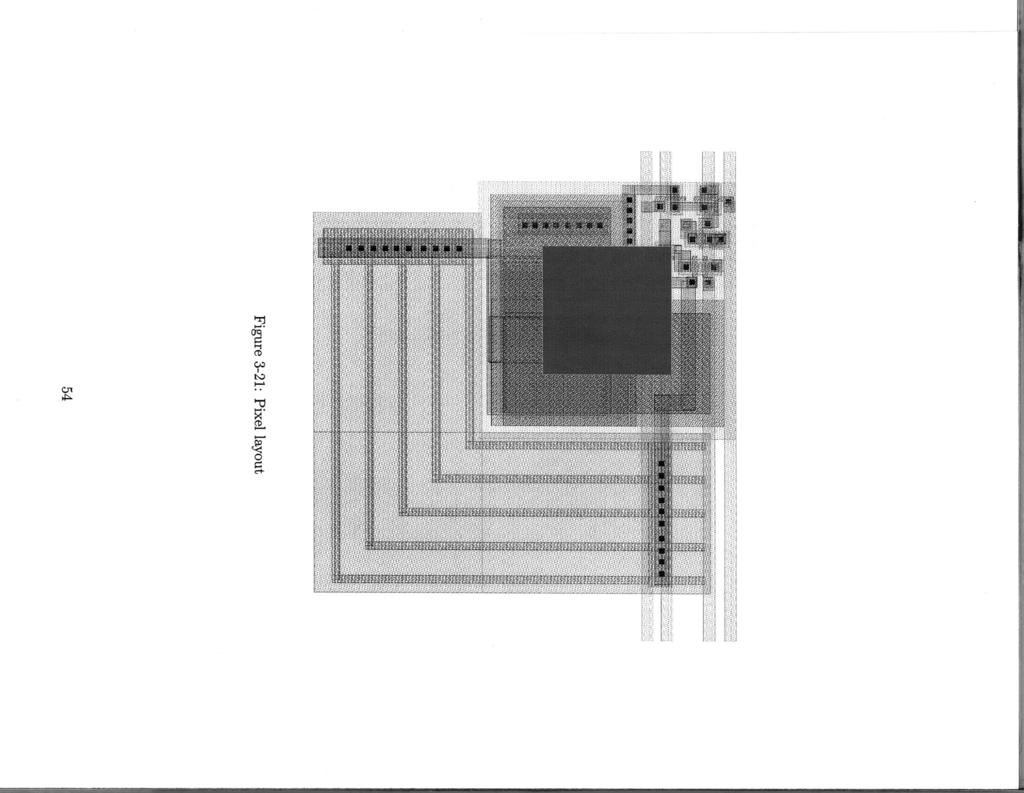
10 3-21 P ixel layout C hip layout Bypassing the primary drive op-amp to drive the pixel column directly Probing the output of the sensor directly
11 List of Tables 3.1 Measured OLED response data D evice Values Primary gain amp design values Feedback op-amp design values Sensor Response
12 12
13 Chapter 1 Introduction Portable electronics are quickly becoming an integral and omnipresent part of our public and private lives. From camera cell phones to digital hand held video recorders, we are inundated with products most people would not have dreamed possible just fifteen years ago. And yet manufacturers of consumer electronics are not closed to finished, promising even further integration of digital tools and toys into our daily lives. This dramatic progress has been largely due to rapid advancement in integrated circuit technology. However, other components of portable electronic devices have not developed or improved as quickly. The designs for such components generate bottlenecks in our passage into a mobile information age. Display technology is an example of one of the principle challenges in developing mobile electronics. Power hungry, heavy and space-consuming, designers are always looking for ways to improve the performance and efficiency of their displays whether they are for labtops or simply cell phones. 1.1 Thesis Objectives This thesis aims to explore the possibility of using Organic Light Emitting Diodes (OLED) as a display technology. An integrated circuit is designed and built to drive an OLED display using pixel by pixel optical feedback. This technique addresses 13
14 the nonlinearity of OLED devices, mismatching between devices, and performance degradation over the device lifetime. 1.2 Thesis Motivation The principle requirement on portable displays are that they be slim and consume as little power as possible. The most common solution today, frequently appearing in notebook/palmtop computers, are liquid crystal displays (LCD). However, LCDs are typically highly inefficient and frequently have a limited viewing angle. Typcial efficiency of an LCD display is roughly 1 lm/w (lumens/watt). OLEDs function much like forward biased LEDs in silicon. Light is emitted as a function of the current through the device. As a direct emission technology, OLEDs appear to be an affordable, highly efficient alternative. The best efficiencies of OLEDs are 5 lm/w for blue OLEDs, 600 lm/w for green OLEDs and 15 lm/w for red OLEDs. [1] In the hopes of realizing the potential advantages inherent to OLED displays, many researchers have worked to find practical solutions to their shortcomings. But the development of OLED technology is behind that of LCDs. First and foremost, building OLEDs with operating characteristics and a lifetime suitable for commercial use has proved elusive. It was not until 1987 that the first vacuum-deposited OLEDs with low operating voltages were demonstrated. [2] Researches have found that various forms of encapsulation of OLEDs can extend their lifetime by as much as two orders of magnitude. Research suggests that devices' continual operation lifetime could easily exceed 1000 hours. [3] However, the power-efficiency curves and I-V relationships of OLEDs are extremely difficult to match between devices. Moreover, both of these characteristics will degrade over a device's lifetime. None-the-less, work has been done to develop flat panel OLED displays. Much of the prior work has concentrated on driving a fixed current through each OLED to avoid voltage threshold variations. [4] This thesis aims at developing a feedback mechanism to control optical light output via an integrated circuit. This is a direct continuation of similar work done in a thesis by Eko Lisuwandi, who developed a 14
15 discrete version of a similar circuit. [5] This thesis seeks to advance that work and demonstrate the feasibility and scalability of using optical feedback implemented in a silicon integrated circuit to control OLED displays. 1.3 Organization Chapter 2 contains a discussion of OLEDs, their advantages, disadvantages and the technique we will use to address their shortcomings, namely opitcal feedback. In Chapter 3, the integrated circuit design will be discussed and specified. The analog feedback loop and its components will be addressed in detail and the digital control aspects of the design will be dealt with briefly. Simulated circuits' performance will also be mentioned. Chapter 4 contains a discussion of the test setup and results. The thesis concludes in Chapter 5. 15
16 16
17 Chapter 2 Organic LED displays OLEDs are an exciting new technology, but certain aspects of their performance leave a lot be desired. 2.1 Advantages As one of the dominant technologies on the market today, LCD displays are contrasted with OLEL)s. A basic LCD display is composed of a liquid crystal material sandwiched between two polarized layers. The liquid crystal material itself is polarized, and its optical axis can be rotated with the application of an electric field across the material. When the optical axis of the liquid crystal is aligned with the other polarizers, light passes through freely. When it is rotated 90 degrees, no light is able to pass through. This technology works well enough, but it has a few problems. The liquid crystal is not a direct emission technology; it does not emit light on its own. In order for the LCD to generate an image some other light source must be employed. Unfortunately, the polarizers and liquid crystal layers may absorb as much as 50 percent of the light on their own. Overall, the light output of the display may be as low as 5 percent of the light generated by the source. This means the display is very inefficient and power hungry. Additionally, the optical properties of the liquid crystal and polarizers distort the image at sharp viewing angles reducing the effectiveness of the display. 17
18 The principle advantage of OLEDs is that they are a direct emission technology. As such, they directly address both of the limitations posed by LCDs. Overall, it is believed that OLED based displays could be brighter, thinner and lighter than LCDs, while solving the viewing angle problem. Furthermore, OLEDs can be made out of transparent materials, allowing them to be viewed from either side or used in a headsup display. Transparent OLEDs can also be stacked, so blue, red and green OLEDs do not share space at each pixel, but lie on top of one another, each fully visible. Finally, the thickness of an OLED structure, typically less than a micrometer, allows for mechanical flexibility, holding the potential of flexible, and thus more portable, displays. [61 One might wonder why if OLEDs are so promising, LEDs are not promising as well. There are, however, a variety of difficulties posed by LED technology that limit their practicality in the development of visual displays. The principle difficulty with LEDs is that it is still very challenging to generate certain colors, particularly blue. Any full color display would surely require three colors, blue being one of them. Blue LEDs have been made, but it is not feasible to piece together displays, pixel by pixel with discrete components. The color of LEDs are closely linked to their material composition and a standard CMOS process would not suffice to produce the different desired colors. This is where the problem lies. It is unclear what, if any, process would be able to support all of the necessary colors. And if it could be done, it would surely be prohibitively expensive. So the lack of LED displays should not disabuse us of the feasibility of an OLED display. OLEDs do not possess the same limitations. 2.2 Disadvantages Unfortunately, there are drawbacks to OLEDs as well. Principally, the I-V characteristics of OLEDs tend to vary dramatically from device to device due to variations in the organic layer thickness, [7] making it very difficult to build drivers that can consistently produce the same optical output from different OLEDs with the same input. Furthermore, OLED performance is substantially affected by the operating 18
19 temperature. [8] Finally, OLEDs tend to degrade over time at differing rates, [9] producing greater non-uniformity in optical output and shorter device lifetimes. 2.3 Optical Feedback To address these difficulties with OLEDs, this thesis proposes to use optical feedback to correct for nonlinearities or variations in OLED optical output. Using photodiodes as sensors and a reasonable amount of gain in the feedback loop, OLED performance should only be limited by performance of the photodiode Control at the Array Level In this design we would like to have direct optical feedback for each pixel on an individual basis. In the simplest approach, we would have a feedback loop laid out around and under each pixel. However, we are designing the electronics for an OLED display laid out on the top of an integrated chip. If we are going to demonstrate the scalability of such a design the display should be at least 16 pixels by 128 pixels. Given the size of an integrated chip, this means the projected pixel size would be microns on a side. That is not a lot of area under each pixel, and it would be a tremendous disadvantage to have a lot of non-transmitting area around each of the pixels, producing a small fill factor. Since it is therefore not possible to place a feedback loop at each pixel, our design must have a minimum of electronics at each pixel with the feedback generating circuitry outside of the array. Further, it is likely that the parasitic power dissipated by the circuit will be proportional to the number of op-amps in the feedback networks. If there is a feedback loop at each pixel, that power will scale as the number of pixels. With a feedback loop per column, that power only scales as the square root of the number of pixels. Since power dissipation is a principle concern in any display, this advantage in scalability is significant. Instead of a feedback loop per pixel there will be a feedback loop per column. To generate a single image, all of the rows are selected one after another, with each feedback loop driving one pixel in that row. The voltage necessary to generate the 19
20 desired optical output is found and then stored until the next time the row is selected. For an effective display, the refresh rate will be determined by the time it takes to cycle through all the rows. This time will be the settling time of the feedback loop multiplied by the number of rows. To increase the refresh rate one must decrease the settling time Circuitry at the Pixel Level The aim is to use a minimum number of components at each pixel. Our design choices reflect that goal. A schematic is shown in Figure 2-1. There are only thre transistors driving the OLED. The first two, MI and M2, are the row select switch and a dummy transistor to reduce charge injection on the gate of M3. M3 is set up as a transconductance amplifier. The key feature in this topology is that the principal limiting factor in the response time of the OLED is the small signal capacitance of the OLED in parallel with the output resistance of the transistor. The pole thus generated will drive the design of the rest of the feedback circuitry. Rough estimates place the pole in the lowest case to be 100 khz. Also needed at each pixel is a photodiode, which functions as a sensor mechanism. In reverse-bias, a photodiode's reverse current is linearly related to the amount of light incident on the photodiode. Our photodiode will draw current from the capacitance at the gate of M5. When M6 is switched on, M5 is driven by a current source provided to the entire pixel column. The current source is not shown in the pixel schematic. M5 acts as a source follower and the sensor output tracks the gate of M5. This allows the sensor to drive the capacitance on the line all the way back to the rest of the feedback circuitry. M4 acts as a switch allowing the capacitance on the gate of M5 to be reset to ground while the sensor is not being used. A miniature simplified version of the array is seen in Figure
21 Driver Input OLED Sel ect M1 T OLED Selet DLED Vdd LM3Vd Vss Vdd Feedback Select M6 Sensor Output Charge Reset l M4 M5 Figure 2-1: Circuit diagram of a pixel Analog Input Analog Input Analog Input Feedback Select r ~Vref=-2.SV rvrel.2.5v rvmf=-2.5v 0LED Select +5V +5V +5V +SV. 5 +5V V 5 Re +5V +5V +5V V +5V +5V I.5V +5V ~ -V5V '~r~ +5V +V+5%' 1 + A +SV +;V + - Figure 2-2: One feedback loop per column 21
22 22
23 Chapter 3 Circuit Design The OLED display driver was designed with both analog and digital circuitry. The control for the system is a continuous time analog feedback loop. The loop employs op-amps with switched capacitor filters. The display array requires a digital row address circuit and the pixels require four digital control signals, with proper timing. 3.1 Analog Feedback Loop The feedback loop links the output from the photodiode sensor to the OLED current driver. There are three important requirements for the feedback loop. It must be stable. It must compensate for the OLED's nonlinearity. And it must have a settling time fast enough to allow for an adequate refresh rate on an OLED display. However, any design must address the constraints posed by the OLED and sensor networks Design Constraints The primary design constraint in the feedback loop stems from the response time of the OLED. Although the voltage-current relationship of the OLED is highly nonlinear, it can be modeled as an equivalent small-signal resistance (ROLED) at any bias point. Moreover, its response time can be modeled as an equivalent capacitance (COLED) in parallel with ROLED. Given these values and the output resistance of the transistor 23
24 Vdd Vdd 9mVgs OLED COLED ROLED Figure 3-1: A visual explanation of the small signal model used for the OELD driving the OLED (rout), the response time of the OLED can be modeled as a pole appearing at the following frequency, 1 2 IUCOLED( ROLED rout) (3.1) Measured data from OLEDs gives an approximation of where this pole will appear. Data is shown in Table 3.1. Capacitance should be increasing linearly with OLED area and resistance should be inversely proportional to OLED area. The pixel area in our array will be roughly 30 microns in diameter. Scaling properly for OLED area, COLED ~ 160fF and ROLED ~ 1OMQ. The output resistance of the silicon transistor is Table 3.1: Measured OLED response data 1mm in diameter 0.25mm diameter Voltage Cap (pf) I Res (KQ) Freq (KHz) Cap (pf) Res (KQ) Freq (KHz)
25 1 rout = (3.2) Ald Each pixel only requires nanoamperes of current, so the transistor driving the OLED will be biased in the subthreshold region with a very high output resistance. At the largest expected current drive of 10 na, HSPICE simulation gives an rout = 30MQ. Thus it is safe to approximate the position of our pole as 1 f = (3.3) 2 i-froledcoled Based on our data, this value is about 100 KHz and is independent of the OLED area, thus fixed by the technology. However, substantial variation is expected in these parameters from device to device so the feedback loop design must be robust with respect to the exact frequency of the pole. Given the response time of the OLED, there are two options for the remainder of the feedback loop. The first is to use the OLED as the dominant pole in the feedback loop and to push all the other poles in the system above the crossover frequency to insure stability. However, the amount of compensation provided by the feedback loop is proportional to its open loop DC gain. Even if this value were as low as 100, with the dominant pole occurring at 100 KHz, the crossover frequency would be at 10 MHz. In order to insure stable operation for a range of OLED response times, the remaining poles in the system would probably have to occur at 30 MHz or higher. Since TSMC's 0.35 micron process was chosen for the project, that is is a fairly stringent requirement for a low power circuit. Fortunately, other options exist. The second option is to introduce a dominant pole at a low frequency and aim for a crossover frequency of 100 KHz while pushing the rest of the system poles above 1 MHz. This has the benefit of providing for stable operation for a wide range of OLED response times while presenting easier specifications to meet for the rest of the feedback loop. The difference from the first option will be that the settling time will be much longer. However, it will still be fast enough. The required time to settle for each pixel row is given by, t = 1/(refresh rate * number of rows). In the display 25
26 0 Light Output G(s) Feedback Figure 3-2: A simple look at the feedback loop block diagram there are 128 rows. Even with a refresh rate of 100 Hz, there are still 80 pas for the feedback loop to settle. A single pole system with a crossover frequency of 100 KHz will settle with a time constant of 10 pus. Adding a pole at the crossover frequency will actually improve the settling time as long as the phase margin does not get worse than 45 degrees. So the feedback loop should have enough time to settle. For these reasons, the second option was chosen for the design of the feedback loop. With this choice, the feedback loop should be stable and have an adequate settling time. The other principal requirement is that our feedback loop provide good control over the output of the OLED. If the feedback loop has a forward transfer function of A(s) and feedback transfer function G(s), then the closed loop transfer function is H (s) = A(s) A~)(3.4) 1 + G(s)A(s) A(s) includes the transfer function of the OLED, which is expected to vary from device to device and degrade over time. G(s) represents our sensor network and feedback circuit. The transfer function of the feedback circuit should be well known. Ideally, each sensor would have the same response to the light emitted by the locally positioned OLED, though this may prove not to be the case. However, the response of the sensor will not change over time and we can determine G(s) by measuring it for any given pixel and calibrate the display accordingly. To function as a display, the light output from the OLED does not need to track a rapidly fluctuating input voltage. Given a fixed input voltage, the OLED needs to settle at a predictable light output within the alloted time slot before the array 26
27 Current Reference Voltage Vdd Incident Light Vdd Sensor Output Reset(Vdd) 0-cjC gs Figure 3-3: A simple circuit model of the sensor output switches the feedback loop on to the next pixel row. For this proportional control H(s) must be constant with respect to s at low frequencies and well known. If for small s, A(s)G(s) > 1, H(s) 1/G(s). Then if G(s) is constant and well known at low frequncies, the condition will be satisfied. Given this requirement, our sensor presents us with our second design constraint. In order to satisfy the conditions on G(s), the feedback loop must compensate for the transfer function of the sensor. The light incident on the photo diode is proportional to the current through the diode. But that current is integrated by the capacitance on the gate of our source follower buffer. So the output voltage of the sensor is proportional to the integral of the light incident on our diode. Vo= Ji ce(t) dt (3.5) gs Since H(s) ~ 1/G(s), if G(s) contains an integrator, then H(s) will contain a differentiator. Then the light intensity will be proportional to the rate of change of input voltage. This is not the proportional control we are looking for. 1/G(s) must be constant for small s so that the system can generate a predictable light output for a given input voltage. Thus, the feedback loop must include a differentiator to cancel this integrator. 27
28 Lastly, the DC gain of the system must be large enough to insure that the approximation, H(s) = 1/G(s) is a good one. In actuality, A(s) H(s) = 1 (s) (3.6) 1 + G(s)A(s) When the open loop gain, A(s)G(s), is much larger than unity we get I I H(s) = - I- (3.7) G (s) - A(s)G(s)) If G(s) is known, the output H(s) can be predicted to the accuracy of the lower bound of the inverse of A(s)G(s). If this value is greater than, for example, 500, we will get 9 bits of accuracy and the accuracy will likely be limited by the precision of our sensor, not the feedback control. Furthermore, suppose the performance of the OLEDs does vary. Let A(s) = aa'(s)) and oz 1 I+ E. If e is small compared to unity, then H(s) = ( 1 (3.8) G(s) A'(s)G(s) AH(s) G(s) A'(s)G(s) (3.9) The matching between devices is then related to the variation term E divided by the open loop gain. As the OLEDs age, A(s) will get smaller. Then we have H(s) = 1 ( - ) (3.10) G (s) ( aa'(s) G(s) As a drops, our control will be reduced. However, if our DC gain is 1000 and a drops to 0.1, which would correspond to a drop in OLED efficiency by an order of magnitude, the output will still be accurate to within 1 percent. This suggest that a DC gain of 1000 should be enough to observe the benefits of feedback control. Larger would be better, but an increased DC gain would require shifting the dominant pole to an even lower frequency. This can be difficult on an integrated chip. 28
29 Vdd Primary Gain Amp yin. ±- Vdd Vdd 'ref o-c OLED Reset OA AE Photodiode cg gs I I Feedback Op-Amps 10R 120R2 Vref Vref Vref Figure 3-4: The circuit model of the feedback loop Loop Parameters The feedback loop is shown in Figure 3-4. The actual circuit uses switched capacitor filters instead of resistors, but the transfer function was designed to match. The opamp operating in open loop has a gain of roughly 1000 with a cross over frequency of 100 KHz, The rest of the feedback loop is designed to have a gain of at most 1 with any parasitic poles occuring well above 100 khz. The gain from the voltage on the gate of the transistor driving the OLED to the current out of the photodiode was estimated based on the g.. of the transistor at the expected current drive, the observed efficiency of the OLEDs and the estimated efficiency of the photodiode detector. The gain from the current out of the photodiode to the output of the differentiator is RiC/Cs. The last two gain stages together have a gain of 100. If the OLED and photodiode operate at the upper range of their approximated gain, then the open 29
30 Table 3.2: Device Values Component I Value C1 4 pf C2 I pf RI 100 K R2 300 K loop transfer function of the overall feedback loop will have a cross over frequency of 100 khz and the loop will be stable. If the gain is less, the cross over frequency will be less than 100 khz so the loop will still be stable. Of course, this will also mean the system settles more slowly. If our settling time is too long, the display will have an unacceptably slow refresh rate. However, it is better to have a slow refresh rate than an unstable feedback loop. In estimating the gain, it is best to insure stability and worry about improving settling time in later design iterations after the response time and gain of the pixel is better understood. In terms of the actual design process, knowing that some feedback compensation would be necesary, I made a first pass at designing the feedback op-amp and observed that a gain-bandwidth product of roughly 100 MHz was achievable. Then I designed the compensation network knowing the requirements the feedback loop as a whole placed on the compensation network but also the likely limitations of the op-amp I would be using. C 1 is chosen to be as large as is reasonable given layout area constraints. This reduces the gain requirement for the rest of the feedback loop. To stabilize the differentiator circuit itself, a capacitor, C 2, is included in the differentiator's feedback loop so that the gain levels off at 1 MHz. This will appear as a pole in the feedback loop's transfer function at 1 MHz- well above our 100 khz cross over frequency. Two additional gain stages were included with a gain of 10 each. If the gain bandwidth product of the op amps used is greater than 10 MHz, then the poles generated by those stages of the feedback loop will be greater than 1 MHz. 30
31 3.1.3 Behavioral Modeling The feedback loop was initially simulated in Matlab using simple block diagrams representing the principal poles and zeroes in the loop. Varying the position of the pole generated by the RC time constant of the OLED from 30 khz to 300 khz, the loop was verified to be stable for a range of OLED response times. Settling time varied from microseconds. The feedback loop was later simulated in HSPICE using op amps with resistors in the feedback path. This allows the simulation to incorporate parasitic poles generated by the finite gain bandwidth product of the op amps without requiring time consuming transient analysis. In the simulation with op amps and resistors, the feedback loop was again found to be stable for a range of OLED response times. 3.2 Op-Amp Design The two basic functions that op-amps perform in the feedback loop require the design of two different op-amps. The requirements for each op-amp are similar, however, so it was possible to design both op-amps with the same topology, but different device parameters Topology A two stage op-amp with an output stage was chosen chiefly for its simplicity. The only specific constraint is bandwidth. The Miller-multiplied capacitor appearing in the common-source amplifier stage of a two stage op-amp allows us good control over the bandwidth and cross-over frequency of an op-amp. Principal secondary concerns are offset voltage, power consumption, noise and slew rate. Basically, power consumption, offset voltage and noise should be minimized while maintaining a sufficient slew rate. Noise in a two stage amp is minimzed by proper device sizing in the input stage. The current in the final leg of the amplifier effectively determines the amp's slew rate. Increasing it improves the slew rate. How- 31
32 Vdd Vdd Vdd Vcurr 1 e 7 M5 M7 M9 M1 V inplus E C - Vout 0- A M2 - - dom Vinminus MZ M8 M3 M4 M6 Figure 3-5: Two stage with output stage op-amp toplogy ever, minimizing power consumption requires there only be one such higher current stage. In a two stage amp, however, a gross current mismatch between the legs forces odd device sizing to keep the voltage offset low. This may include using non minimal transistor lengths, which tends to reduce the bandwidth of the amp and is thus undesirable. At a minimum cost in area we can include an output stage. Then we have three power-consuming current legs, but two of them are low current, so the increase in power consumption is minimal. Device sizes can be adjusted to give effectively zero systematic offset voltage in simulation. Of course, in reality, device mismatch from fabrication will generate some offset that is then determined by the degree of mismatch and the open loop gain. The output stage has the additional benefit of providing a lower output resistance. This will help avoid generating a pole at a low frequency if we operate the op-amp in closed loop with a capacitor in the feedback loop Primary Gain Op-Amp The primary gain op-amp is intended to provide the DC gain for the feedback loop as a whole and to set the cross over frequency for the system by introducing a low frequency pole. Glancing at the schematic, this op-amp appears to be operating open 32
33 Table 3.3: Primary gain amp design values Transistor] Length(pm) [Width(pum) Ml, M M3, M M MZ M M M8, M loop. In actuality, the feedback loop for the op-amp is the overall feedback network. To decide on device sizes I started with minimum device sizes and adjusted as was appropriate. The reference voltage is intended to generate 1 pa of current through M5. The noise will increase as you decrease the current. Additionally, at lower current g, is reduced, causing secondary parasitic poles to be more likely a problem. On the balance, 1 pza will be small compared to the 5-8 pa that will be running through the output current leg. Increasing the bias current will cause the op-amp to consume significantly more power. Further decreasing the current will not substantially reduce the power consumption of the op-amp but may lead to other problems. The primary gain op-amp is designed to generate the needed open loop gain. A two stage op-amp should have a gain that is roughly (gmr ) 2. This should be enough to give us the desired DC gain of about The precise gain is not particularly important so the device values were not chosen with it in mind. However, the crossover frequency of the primary gain op-amp must be controlled carefully. Assuming the Miller multiplied capacitor generates a dominant pole capacitor, hand analysis gives the following important op-amp equations: g, m+gm 2 Adm = gm6(ro6ir o 7) 2 (r. 2 Iro 4 ), gm1 = 9 m2 1 fe = Admf3dB, f3db - 27rRC C = Cdogm6(r.61 rio), R = ro2 1r o4 33
34 fc = 2,Cd 9 g 1 = 2(W/L)IpCPId Given that fc must be 100 khz, it is probable that a large Cdom will be necessary. However, there will be one feedback loop per column of any display. With a desired pitch of microns, large, space-consuming capacitors should be avoided. Instead of increasing Cdm further, it is possibly to reduce Ymi instead. The width is already the minimum size. It is also undesirable to reduce the current any further, in this case, because charging and discharging Cdom could prove to be the limiting factor in the slew rate of the op-amp. But lengthening the transistors can also reduce gmi. You can approximate the chip area required for the desired cross-over frequency. expanding and grouping terms, gmroav2 (2irrC) fc = = C 2Id(WL)PnCox = cvit L = 7(3.11) C2 Equation 3.11 describes the relationship between the length of the transistors in the input stage and the compensation capacitor required to keep the cross-over frequency constant. You can increase C, but then you would have to decrease L, and vica versa. We can use this relationship to determine the C and L that will minimize our area in layout. The answer is independent of the constant factor -Y, which is why it is unimportant. Based on the general layout chosen, let the area taken up by the transistors be given as al and bc be the area consumed by the compensation cap. Both of these are assumed to scale linearly with L and C, as one would expect. Since L and C are related, we can express one in terms of the other. Area = al + bc = a + bc C2 34
35 d Area dc 2ay C3 2ay b2_ C = L = b 4a 2 2aL = 2ab 2 = bc (3.12) As can be seen by our result in equation 3.12, it doesn't matter what the constants a and b actually are. But if you minimize the area with respect to the capacitance, you will find that the contribution to the area from the device lengths should be half that of the contribution from the capacitance. So in any given process or layout configuration you can optimize this without too much trouble by at least approximating those constants. In our case, MI and M2 are longer devices and their specific lengths were determined by the op-amp bandwidth requirement and the layout configuration I chose. Now the gain of the first stage is gm 2 (ro 2 1Iro 4 ). Since r, = 1/(AId) and A c 1/L, ro Oc L/Id. Thus, as we increase the length of M1, gmi decreases, but rol increases. To maintain the desired DC gain in the op-amp, it is necessary to increase the lengths of M3 and M4 as well, so that ro 4 increases with ro, and the DC gain remains high. The DC gain of the op-amp is also related to the gain of the common source amplifier stage. The gain of this stage was maximized by using the minimum current (1pA). The width of M6 was adjusted so the voltage needed on the gate of M6 to avoid railing the output of the op-amp was matched to the voltage provided by the first stage. We can approximate this using hand analysis and comparing the current through M4 and M6. Assume that since the current through M3 and M4 are the same and V, - V, for M3, the same holds for M4. Then if Id 4 (L 4 /W 4 ) = 1d6(L 6 /W), Vs for M6 shouldn't have to rail one way or the other to supply the necessary current through M6. However, variations in V, the actual voltage present on the drain of M4, and the actual currents in the two legs prevents our hand analysis from matching HSPICE results in this case. The relationship Id6 oc W 6 /L 6 for a fixed V, is still useful with the aid of HSPICE in finding a width that minimizes the op-amp's offset. 35
36 The output stage is simply designed to carry a slightly higher current to drive larger output loads. The primary driver amplifier has to drive the entire column of pixels beneath it which will include a lot of parasitic capacitances. Finally, a two stage op-amp using a Miller compensation cap will have a zero at s = 9m. By adding a series resistance, we can move this zero to s = 9,61/R. MZ is sized and biased to generate a resistance to move this zero into the left half plane. The sizing and biasing are done almost entirely using HSPICE. The transistor is connected to the output of the first stage. The gain through the second stage is roughly 30. Thus the variation in the output of the first stage will be 30 times less than the output of the second stage and the bias conditions of the transistor will not be changing very much Feedback Op-Amp Ignoring the contribution from the primary gain op-amp, the feedback loop should have unity gain with a flat frequency response. The topology is the same as for the driver amp, shown in Figure 3-5. The transfer function of the OLED driver and optical sensor will require additional gain and a differentiator. The feedback op-amp will be used in a few simple op-amp circuits to implement these functions. Once the paramters of the comensation network were decided, I went back and finalized a design for an op-amp that would function in the feedback loop. Using the design of the primary gain op amp as a starting point, I adjusted accordingly., First, the unity gain frequency of the op-amp needed to be maximized while maintaining closed loop, unity gain stability. So a large compensation capacitor and longer transistors were not needed. Furthermore, a two stage op-amp would easily have 60 db of gain. That is enough so that the accuracy of the desired gain in closed loop is a function of the matching between the capacitors or resistors in the closed loop not the finite gain of the op-amp. A current of 1 pua was sufficient in the first two stages to push parasitic poles resulting from the capacitance on the gates of M3 and M4 or at the gate of M8 well beyond the 100 MHz crossover frequency of the amplifier. This is not surprising 36
37 Table 3.4: Feedback op-amp design values Transistor Length(pm) I Width(pm) M1, M M3, M M MZ M M M8, M because the equivalent resistance at those nodes is 1/gm3 and 1/gm 6, respectively, which will be relatively small. The output of the op-amp may also be loaded with a capacitor because the op-amps will be connected with switched capacitor circuits. The output resistance of the op-amp is 1/gms. By increasing the current and width of this device by a factor of 4, the output resistance is correspondingly decreased. This helps to insure that any pole generated by that output resistance and an output load capacitor will at frequency higher than the cross-over frequency of the amplifier. Moreover, the higher current will result in a higher slew rate, which is important for transient settling times in a switched capacitor circuit Op-Amp Simulations Both op-amps were simulated using HSPICE. Since the design is for TSMC's 0.35 micron process, I used the libraries available in the CMC design kit. Using an open loop AC analysis with the output load the op-amp will be driving, it is possibly to determine both the bandwidth and the phase margin of the op-amp. A closed loop AC analysis of the feedback op-amp can verify stability in the feedback configurations that the op-amps will be used in and that the desired transfer functions will be generated. The driver op-amp needs to look like a single pole system. At its cross-over frequency of 81 khz it has 91.3 degrees of phase delay as seen in Figure 3-6. At 100 khz it has only a few more degrees of delay. Thus it has the desired cross-over frequency and appears as a single pole system in the frequency range of interest. 37
38 The stability of the feedback op amp is shown in Figure 3-7 with 68 degrees of phase margin. In closed loop with constant gain, the feedback op-amp should look like an inverter with 180 degrees of delay. At 100 khz it has only one extra degree of delay as shown in Figure 3-8. As a differentiator, the feedback amp should have 90 degrees of delay. This is also the case; at 100kHz it has approximately 94 degrees of delay, as shown in Figure 3-9. U, 102 =-- C 0) I I I IU CO I i Frequency Figure 3-6: Bode plot of the driver op-amp in open loop 38
39 10 I c ~ -200 L Frequency Figure 3-7: Bode plot of the feedback op-amp in open loop 39
40 10 - E ~ -11L (D 120-.C Frequency Figure 3-8: Bode plot of the feedback op-amp in closed loop with a constant gain 40
41 10' ) Ca 0- a i Frequency Figure 3-9: Bode plot of the feedback op-amp as a differentiator 41
42 A C A V1., <V2 B *B Figure 3-10: An example of a switched capacitor 3.3 Switched Capacitor Networks Since it is very space consuming to have large poly resistors in CMOS, a switched capacitor filter is employed in the feedback loop. The capacitors also have the advantage of better matching over poly resistors. The basic idea is that charging a capacitor and then discharging it across two nodes will generate an effective resistance at signal frequencies that are small compared to the switching frequency Basic Switched Capacitors The basic idea is shown in Figure First, the two switches governed by B are open and those governed by A are shorted. The voltage across C results in an accumulated charge. Then the switches governed by A are opened and the switches to ground are shorted. The charge across the capacitor is dissipated through ground. If f is the switching frequency we have the following: Q = (V1 - V2)C, I=, I = f(v1 - V2)C 6t 6V 1 Refjf = C (3.13) In practice, the switches are replaced by transistors. One might hope to implement a switched capacitor network simply by replacing the resistors in the circuit with switched capacitors as shown in Figure Unfortunately, it is not so simple. Assuming the presence of an ideal op-amp and ideal switches, there is nothing wrong with the circuit shown. However, when A is low and those transistors act as open cir- 42
43 A C -1-- A A B Vin *~ Vout Figure 3-11: A naive switched capacitor circuit implementation cuits, the op-amp will be operating in open loop. And when the transistor connected to the inverting input of the op-amp is closed, a small amount of channel charge will be injected onto the gate capacitance of the input. In open loop, this small voltage offset will generally be large enough to rail the output of the op-amp. This has two effects. First, the output will only be accurate while A is low. There are techniques to address that problem. But worse, when A goes high again, the op-amp's transient settling time will be limited by the slew rate of the amplifier. And with the output fully railed, that time will be considerable. Given that the cross-over frequency of the op-amp is 100 khz, we need to insure that switching network has no adverse effect on the feedback loop transfer function at frequencies smaller than 100 khz. Likely, a switching frequency of 3-10 MHz will be required. This would require the settling time to be substantially less than 100 ns. Without dissipating significant power, there is really no way to recover the output so quickly Actual implementation Fortunately, an alternative approach does exist. Placing actual capacitors in parallel with the switched capacitors insures that the op-amp will never be in open loop. The schematic is shown in Figure Charge will still be injected on the gate during each cycle, but the feedback will prevent the op-amp from saturating. Of course, adding capacitors should change the transfer function of the circuit. But actually, to 43
44 first order, it remains the same. In the inverting configuration used, let Z 1 denote the input impedance and Z 2 denote the feedback impedance. t - Av V, m -=Z 2 Vin + Z 1 Vout Z1 + Z2 Vou _ AvZ 2 (3.14) Vin Z 1 + Z 2 + AvZ 1 if AvZ 1 > Z 1 + Z 2, then V- =- (3.15) Vin Z 1 Hi(S) 1/(fC) 1 1/(sC + f C) - 10 VS (3.16) 1/(f l0c) ' 1/(s10C + f l0c) Thus, at lower frequencies where the assumption that the gain of the op-amp will be large is true, the transfer function will be unchanged. Given that our op-amps have a gain--bandwidth product of 100 MHz, with a closed loop gain of 10, this should be true up to 10 MHz. At this point, one might wonder why we cannot just use the capacitors by themselves without the switched capacitors. The problem is that the inverting input to the op-amp will have no dc path to ground. That is, any charge on that node will have no opportunity to dissipate and a corresponding voltage offset will result. The switched capacitors allow us to dissipate any such charge. However, an offset will still result from accumulated charge at the inverting input of the op-amp. Each clock cycle, additional charge will be injected at the inverted input as the transistor connected there switches off. We can approximate the output offset as a function of the charge, Q, injected during each cycle. If the input voltage remains fixed, then in steady state, any charge injected onto the input when A drops, will be removed when A is high. First, note that the simple capacitor connecting the output and inverting input, C1, is Miller-multiplied by the gain of the op-amp. Thus it is effectively substantially larger than the input capacitor. Any charge removed from the inverting input will be removed almost entirely from C1. Thus, a corresponding 44
45 10C C A C -- Vin A A Abar B 1 10C 1 7 IF1F W W/2 Vout B B Figure 3-12: Actual switched capacitor circuit implementation charge must be injected onto the other side of C 1, at the output of the op-amp. If Q charge is injected onto the node as A drops, Q charge is removed when A rises. So Q charge is injected from the output onto Ci. Since the inverting input and the non-inverting input will be close to equal in stable feedback, the output will simply by the voltage across Ci, V 1 ff = Q/Ci. The big problem with this offset is that an offset in the first stage of our feedback loop will be multiplied by the following stage. This could rail the signal in the feedback loop, preventing the feedback loop from functioning. This offset can be minimized by increasing C or decreasing Q. The size of C1 is sharply limited by the availability of area. At first pass, Q is minimized by decreasing the size of the transistor switches. Using minimum resistors, the Q was found in simulation to be roughly 3 fc. Suppose C1 = 100 fa, then V 1 ff = 30 mv. But if the first stage of our feedback loop has an offset of 30 mv, and that offset voltage is multiplied by 100, the signal will rail. So additional measures have to be taken. We can actually further reduce Q by using a charge cancellation technique. A simple approach is to include a dummy switching transistor at our sensitive node whose drain and source are shorted to the node. Its width should be one half the width of our actual switching transistor. The theory is that approximately half the channel charge of our switch transistor gets dumped on our sensitive node. The gate of the dummy transistor is attached to an inverted version of the switching signal. 45
46 Vin Cin C C2 A I A Abar B O B Od W W/2 0Vout Figure 3-13: Differentiator Switched Capacitor Network When the switch transistor turns off, the dummy transistor turns on, drawing charge from the sensitive node to fill its channel. Ideally, this would identically match the charge dumped from the real switch. In practice, we can expect Q to be reduced by a factor of 10. This will substantially reduce our output offset. The final circuit for a constant gain stage is shown in Figure The differentiator is show in Figure In addition to using charge cancellation, our feedback loop includes a differentiator. Any DC offset at the input of a differentiator will be blocked because the gain of a differentiator will be zero. Thus, we can move the differentiator to the end of our feedback loop. Then the maximum offset in the feedback loop is the offset in the first stage multiplied by the gain in the second stage (10). And the offset at the input to the primary gain op-amp is only the offset from the differentiator. With this circuit configuration, the offset will be kept sufficiently small. 46
47 S Frequency (rad/sec) Figure 3-14: Magnitude Frequency Response of Differentiator Switched Capacitor Simulations Switched capacitor networks are difficult to test in a circuit simulator because standard AC analysis is not applicable. The transistors switching on and off can not be modeled as linear elements. First, the differentiator is simulated in Matlab assuming perfect switches and a finite gain op-amp. The results are shown in Figure 3-14 and Notice the approximately 90 degrees of phase delay at 100 khz. To test the effect of real switches it is necessary to run transient simulations in HSPICE. The input to the differentiator is a 200mV peak-to-peak 10 khz sine wave. The output is shown in Figure The output is delayed by 90 degrees as we would expect from a differentiator. The output has a lot of high frequency noise on it from all the switching. Fortunately, both the OLEDs and the human eye filters noise above 1 MHz. The input to the constant gain stage is a 20 mv peak-to-peak 100 KHz sine wave. The output is shown in Figure The output is an inverted 200 mv wave with no phase delay. Since the time scale is smaller, the switching noise is more noticeable for the DC gain stage. Also, notice the DC offset. Without using charge cancellation the offset would be unacceptable. The simulation verifies that our stage has a gain of 10 and that any pole occurs well above 100 khz. 47
48 270 CL s 10a 10 Figure 3-15: Phase Frequency Response of Differentiator I C u 10u 150u 200u Time (Bin) (TIME) 250u Figure 3-16: Transient simulation of the switched capacitor differentiator 48
49 1.8- SU 1&U 1u 2Ou 25U Time (11n) (TIME) Figure 3-17: Transient simulation of the switched capacitor constant gain stage 3.4 Row Addressing The system is designed so that there is a feedback loop for each column, and they all operate on one row at the time. There is a set of four digital signals for each row that control when that row is connected to the feedback loop. Each signal has a default value for when that row is not selected. When one desires to set the optical output from a given row, a 7-bit address corresponding to that row is sent to the chip. Then the digital control signals for that row must be set according to four corresponding signals sent to the chip. This setup allows fine tuned control of the control signal timing from off chip. To address the rows, a simple approach would be to have the 7 address bits and their inverse sent to every row. Then each row would digitally AND the 7 bits corresponding to that row, producing a signal that was logically 1 if and only if that row was being addressed. However, this would require either a large 7-input AND gate, or multiple smaller gates. But the rows have a pitch of 30 microns and it could be difficult to fit a large digital gate into the space for each row. Instead, I chose to use a scheme that includes pre-processing of the address, and combines the rows into groups of four, reducing the area needed at each individual 49
50 Address ' Address 0 AddressAs Figure 3-18: Address preprocessing circuits Address 1,2 Address 3,4 Address 5,6 Control Signals One Pixel Row Address 0 To Pixel Row Figure 3-19: Row Addressing Circuit row. First, the address is pre-processed by grouping the address into 3 groups of 2 and one individual bit. Then for each group, a control line representing each logical possibility for the group is run down the side of the pixel array. For example, a group of two bits will have four lines, corresponding to the logical values 00, 01, 10 and 11. Only one of the these lines will be high for any given address input. Secondly, for each group of 4 rows we first consider address bits 0-4. These correspond to three different groups. From each group, we take one logical value. The three values are combined in a 3-input AND gate. Then the last two bits of the address are considered. For each row in our group of 4, a different logical value is combined in a two input AND gate with the output from our 3-input AND. Call this output rowselect. For any given address, only one row will have rowselect be logically high. This value is then combined with each control signal in 4 2-input AND gates. Depending on the default value for the control signal, the output is inverted or not before being sent down the row to the pixels. The 4 2-input AND gates are unavoidable. However, this scheme uses only one 50
51 additional 2-input AND gate for each row and one 3-input AND gate for every four rows. So it should be easy to fit all the gates into the pitch of the rows. Additionally, you would need at the very minimum, 7 address lines running down the side of the pixel array for row addressing. This scheme requires 14 lines and a small amount of pre-processing circuitry at the top of the array. 3.5 Control Signal Timing The four control signals which govern the operation of each pixel. The first two, OLED and OLED control the input to the pixel driving transistor. One is simply the inverse of the other and operates the dummy transistor that is used to reduce the charge injection. The third signal RESET is normally on to pull the gate voltage on the source follower output down to ground while the pixel is not connected in feedback mode. When the signal turns off, the voltage is able to slowly charge back up while the pixel is in feedback mode and current through the photo diode is deposited on the gate. The fourth signal, SENSOR, switches the output from the sensor into the main feedback path. The switching time is not particularly crucial for any of these signals, but their relative timing is fairly important. In order to reduce large transients in the feedback path and to insure the correct voltage is left on the gate of the pixel driving transistor at the end of the cycle, the correct timing must be observed. The first and last signal to switch should be the RESET signal. The feedback loop cannot function properly while it is turned on and there is no harm in turning it off early and turning it on again late. Secondly, the SENSOR signal should be switched on so that the feedback path can begin to settle based on the current OLED output, which should be close to what it is already supposed to be. Last, the OLED and OLED signals should connect the input of the pixel to the main driver line. At the end of the cycle, it is critical that OLED switch off first so that the right voltage is held on the gate of the transistor driving the pixel. OLED should switch at the same time to minimize the charge injection on the gate. Second, the 51
52 Address= Row 1 Row 2 Row 3 OLED OLED7 SENSOR RESET Figure 3-20: Control signal timing diagram for 3 consecutive rows SENSOR signal can safely disconnect the pixel from the feedback loop. And finally, the RESET signal can be turned on again without introducing unnecessary transients in the feedback path. Since these signals are controlling PMOS transistor switches, a logical zero corresponds to an analog value of vdd while a logical one corresponds to an analog value of ground. In addressing the entire pixel array, each cycle of the control signals addresses a different pixel row. Thus the control signal inputs will essentially be digital signals with varying duty cycle and phase. For each cycle/row the correct address must first be entered, the correct control signals set and the correct analog values asserted for each column. The analog values must be held until the end of the cycle, when the control signals switch the pixel row out of the feedback loop and the address changes, moving on to the next row. Going through the entire array, a different analog value may be asserted for each pixel. To generate an image, you would assert the same values for each pixel each time through the array. To generate a changing image, you can change pixel values each time the array is refreshed. 52
53 3.5.1 Layout The layout was done in TSMC's 0.35 micron process. The pixel array dominates the layout. The feedback control loops are situated above and below the array. The dominant constraint in their layout is matching the pitch of the pixel array. The digital address circuitry runs along the side of the array, also matching the pitch of the array. The pixel layout is as tight as possible to allow for a small pixel area. The transistors are clustered in one corner. The pad to contact the OLED rests above the transistors and the capacitor that stores the charge at the gate of the OLED driving transistor. The photo diode is shaped in a backwards L around the pad contact. Since the metal pad is not transparent, there is no point to having the diode under the metal layer. The pads to electrically contact the chip are only allowed on the left side and top. This is due to concerns with regard to the OLED processing stage. There is also an additional pad which runs along the left side of the array and across the top. This is to contact the bottom side of the OLEDs during the OLED processing stage. The very bottom of the chip allows for extra pads since our layout is pad limited. The extra chip area is taken up with extra metal and poly structures to meet fill requirements. The chip dimensions are roughly 6mm by 1mm. 53
54 c-i, C y
Overview of All Pixel Circuits for Active Matrix Organic Light Emitting Diode (AMOLED)
") Chapter 2 Overview of All Pixel Circuits for Active Matrix Organic Light Emitting Diode (AMOLED) ---------------------------------------------------------------------------------------------------------------
Chapter 2 Overview of All Pixel Circuits for Active Matrix Organic Light Emitting Diode (AMOLED) ---------------------------------------------------------------------------------------------------------------
 Chapter 3 Evaluated Results of Conventional Pixel Circuit, Other Compensation Circuits and Proposed Pixel Circuits for Active Matrix Organic Light Emitting Diodes (AMOLEDs) -------------------------------------------------------------------------------------------------------
Lecture 3, Opamps. Operational amplifiers, high-gain, high-speed
 Lecture 3, Opamps Operational amplifiers, high-gain, high-speed What did we do last time? Multi-stage amplifiers Increases gain Increases number of poles Frequency domain Stability Phase margin 86 of 252
EL302 DIGITAL INTEGRATED CIRCUITS LAB #3 CMOS EDGE TRIGGERED D FLIP-FLOP. Due İLKER KALYONCU, 10043
 EL302 DIGITAL INTEGRATED CIRCUITS LAB #3 CMOS EDGE TRIGGERED D FLIP-FLOP Due 16.05. İLKER KALYONCU, 10043 1. INTRODUCTION: In this project we are going to design a CMOS positive edge triggered master-slave
A FOUR GAIN READOUT INTEGRATED CIRCUIT : FRIC 96_1
 A FOUR GAIN READOUT INTEGRATED CIRCUIT : FRIC 96_1 J. M. Bussat 1, G. Bohner 1, O. Rossetto 2, D. Dzahini 2, J. Lecoq 1, J. Pouxe 2, J. Colas 1, (1) L. A. P. P. Annecy-le-vieux, France (2) I. S. N. Grenoble,
T sors, such that when the bias of a flip-flop circuit is
 EEE TRANSACTONS ON NSTRUMENTATON AND MEASUREMENT, VOL. 39, NO. 4, AUGUST 1990 653 Array of Sensors with A/D Conversion Based on Flip-Flops WEJAN LAN AND SETSE E. WOUTERS Abstruct-A silicon array of light
Hello and welcome to this training module for the STM32L4 Liquid Crystal Display (LCD) controller. This controller can be used in a wide range of
 controller. This controller can be used in a wide range of") Hello and welcome to this training module for the STM32L4 Liquid Crystal Display (LCD) controller. This controller can be used in a wide range of applications such as home appliances, medical, automotive,
Hello and welcome to this training module for the STM32L4 Liquid Crystal Display (LCD) controller. This controller can be used in a wide range of applications such as home appliances, medical, automotive,
ECEN620: Network Theory Broadband Circuit Design Fall 2014
 ECEN620: Network Theory Broadband Circuit Design Fall 2014 Lecture 12: Divider Circuits Sam Palermo Analog & Mixed-Signal Center Texas A&M University Announcements & Agenda Divider Basics Dynamic CMOS
Report on 4-bit Counter design Report- 1, 2. Report on D- Flipflop. Course project for ECE533
 Report on 4-bit Counter design Report- 1, 2. Report on D- Flipflop Course project for ECE533 I. Objective: REPORT-I The objective of this project is to design a 4-bit counter and implement it into a chip
25.5 A Zero-Crossing Based 8b, 200MS/s Pipelined ADC
 25.5 A Zero-Crossing Based 8b, 200MS/s Pipelined ADC Lane Brooks and Hae-Seung Lee Massachusetts Institute of Technology 1 Outline Motivation Review of Op-amp & Comparator-Based Circuits Introduction of
DIFFERENTIAL CONDITIONAL CAPTURING FLIP-FLOP TECHNIQUE USED FOR LOW POWER CONSUMPTION IN CLOCKING SCHEME
 DIFFERENTIAL CONDITIONAL CAPTURING FLIP-FLOP TECHNIQUE USED FOR LOW POWER CONSUMPTION IN CLOCKING SCHEME Mr.N.Vetriselvan, Assistant Professor, Dhirajlal Gandhi College of Technology Mr.P.N.Palanisamy,
VLSI Design: 3) Explain the various MOSFET Capacitances & their significance. 4) Draw a CMOS Inverter. Explain its transfer characteristics
 Explain the various MOSFET Capacitances & their significance. 4) Draw a CMOS Inverter. Explain its transfer characteristics") 1) Explain why & how a MOSFET works VLSI Design: 2) Draw Vds-Ids curve for a MOSFET. Now, show how this curve changes (a) with increasing Vgs (b) with increasing transistor width (c) considering Channel
1) Explain why & how a MOSFET works VLSI Design: 2) Draw Vds-Ids curve for a MOSFET. Now, show how this curve changes (a) with increasing Vgs (b) with increasing transistor width (c) considering Channel
The Distortion Magnifier
 The Distortion Magnifier Bob Cordell January 13, 2008 Updated March 20, 2009 The Distortion magnifier described here provides ways of measuring very low levels of THD and IM distortions. These techniques
PESIT Bangalore South Campus
 SOLUTIONS TO INTERNAL ASSESSMENT TEST 3 Date : 8/11/2016 Max Marks: 40 Subject & Code : Analog and Digital Electronics (15CS32) Section: III A and B Name of faculty: Deepti.C Time : 11:30 am-1:00 pm Note:
Switched Mode Power Supply
 Switched Mode Power Supply (DC/DC buck converter) 1-Why use a DC/DC converter? 2-Architecture 3-Conduction modes Continuous Conduction Mode Discontinuous Conduction Mode 4-Stability Voltage Mode Current
Dual Slope ADC Design from Power, Speed and Area Perspectives
 Dual Slope ADC Design from Power, Speed and Area Perspectives Isaac Macwan, Xingguo Xiong, Lawrence Hmurcik Department of Electrical & Computer Engineering, University of Bridgeport, Bridgeport, CT 06604
CCD 143A 2048-Element High Speed Linear Image Sensor
 A CCD 143A 2048-Element High Speed Linear Image Sensor FEATURES 2048 x 1 photosite array 13µm x 13µm photosites on 13µm pitch High speed = up to 20MHz data rates Enhanced spectral response Low dark signal
V6118 EM MICROELECTRONIC - MARIN SA. 2, 4 and 8 Mutiplex LCD Driver
 EM MICROELECTRONIC - MARIN SA 2, 4 and 8 Mutiplex LCD Driver Description The is a universal low multiplex LCD driver. The version 2 drives two ways multiplex (two blackplanes) LCD, the version 4, four
Design and Simulation of a Digital CMOS Synchronous 4-bit Up-Counter with Set and Reset
 Design and Simulation of a Digital CMOS Synchronous 4-bit Up-Counter with Set and Reset Course Number: ECE 533 Spring 2013 University of Tennessee Knoxville Instructor: Dr. Syed Kamrul Islam Prepared by
System Quality Indicators
 Chapter 2 System Quality Indicators The integration of systems on a chip, has led to a revolution in the electronic industry. Large, complex system functions can be integrated in a single IC, paving the
Scan. This is a sample of the first 15 pages of the Scan chapter.
 Scan This is a sample of the first 15 pages of the Scan chapter. Note: The book is NOT Pinted in color. Objectives: This section provides: An overview of Scan An introduction to Test Sequences and Test
Feedback: Part A - Basics
 Feedback: Part A - Basics Slides taken from: A.R. Hambley, Electronics, Prentice Hall, 2/e, 2000 1 Overview The Concept of Feedback Effects of feedback on Gain Effects of feedback on non linear distortion
ML6428. S-Video Filter and 75Ω Line Drivers with Summed Composite Output. Features. General Description. Block Diagram Σ BUFFER.
 www.fairchildsemi.com ML S-Video Filter and Line Drivers with Summed Composite Output Features.MHz Y and C filters, with CV out for NTSC or PAL cable line driver for Y, C, CV, and TV modulator db stopband
Technology White Paper Plasma Displays. NEC Technologies Visual Systems Division
 Technology White Paper Plasma Displays NEC Technologies Visual Systems Division May 1998 1 What is a Color Plasma Display Panel? The term Plasma refers to a flat panel display technology that utilizes
Timing Error Detection: An Adaptive Scheme To Combat Variability EE241 Final Report Nathan Narevsky and Richard Ott {nnarevsky,
 Timing Error Detection: An Adaptive Scheme To Combat Variability EE241 Final Report Nathan Narevsky and Richard Ott {nnarevsky, tomott}@berkeley.edu Abstract With the reduction of feature sizes, more sources
Project 6: Latches and flip-flops
 Project 6: Latches and flip-flops Yuan Ze University epartment of Computer Engineering and Science Copyright by Rung-Bin Lin, 1999 All rights reserved ate out: 06/5/2003 ate due: 06/25/2003 Purpose: This
Monolithic CMOS Power Supply for OLED Display Driver / Controller IC
 Monolithic CMOS Power Supply for OLED Display Driver / Controller IC Cheung Fai Lee SOLOMON Systech Limited Abstract This paper presents design considerations of a power supply IC to meet requirements
CCD Element Linear Image Sensor CCD Element Line Scan Image Sensor
 1024-Element Linear Image Sensor CCD 134 1024-Element Line Scan Image Sensor FEATURES 1024 x 1 photosite array 13µm x 13µm photosites on 13µm pitch Anti-blooming and integration control Enhanced spectral
High Performance TFT LCD Driver ICs for Large-Size Displays
 Name: Eugenie Ip Title: Technical Marketing Engineer Company: Solomon Systech Limited www.solomon-systech.com The TFT LCD market has rapidly evolved in the last decade, enabling the occurrence of large
LM16X21A Dot Matrix LCD Unit
 LCD Data Sheet FEATURES STC (Super Twisted igh Contrast) Yellow Green Transmissive Type Low Power Consumption Thin, Lightweight Design Permits Easy Installation in a Variety of Equipment General Purpose
CS/EE 6710 Digital VLSI Design CAD Assignment #3 Due Thursday September 21 st, 5:00pm
 CS/EE 6710 Digital VLSI Design CAD Assignment #3 Due Thursday September 21 st, 5:00pm Overview: In this assignment you will design a register cell. This cell should be a single-bit edge-triggered D-type
ELEC 4609 IC DESIGN TERM PROJECT: DYNAMIC PRSG v1.2
 ELEC 4609 IC DESIGN TERM PROJECT: DYNAMIC PRSG v1.2 The goal of this project is to design a chip that could control a bicycle taillight to produce an apparently random flash sequence. The chip should operate
Design of Organic TFT Pixel Electrode Circuit for Active-Matrix OLED Displays
 JOURNAL OF COMPUTERS, VOL. 3, NO. 3, MARCH 2008 1 Design of Organic TFT Pixel Electrode Circuit for Active-Matrix Displays Aram Shin, Sang Jun Hwang, Seung Woo Yu, and Man Young Sung 1) Semiconductor and
WINTER 15 EXAMINATION Model Answer
 Important Instructions to examiners: 1) The answers should be examined by key words and not as word-to-word as given in the model answer scheme. 2) The model answer and the answer written by candidate
Clocking Spring /18/05
 ing L06 s 1 Why s and Storage Elements? Inputs Combinational Logic Outputs Want to reuse combinational logic from cycle to cycle L06 s 2 igital Systems Timing Conventions All digital systems need a convention
Optimizing BNC PCB Footprint Designs for Digital Video Equipment
 Optimizing BNC PCB Footprint Designs for Digital Video Equipment By Tsun-kit Chin Applications Engineer, Member of Technical Staff National Semiconductor Corp. Introduction An increasing number of video
Communication and Computer Engineering ( CCE ) Prepared by
 Prepared by") Communication and Computer Engineering ( CCE ) Graduation Project Report Spring 2013 Digital TV Tuner Front End Design Part A : LNA and Mixer Prepared by 1. Ahmed Hesham Mohamed (1082011) 2. Mohamed Khaled
Communication and Computer Engineering ( CCE ) Graduation Project Report Spring 2013 Digital TV Tuner Front End Design Part A : LNA and Mixer Prepared by 1. Ahmed Hesham Mohamed (1082011) 2. Mohamed Khaled
Design and Analysis of Custom Clock Buffers and a D Flip-Flop for Low Swing Clock Distribution Networks. A Thesis presented.
 Design and Analysis of Custom Clock Buffers and a D Flip-Flop for Low Swing Clock Distribution Networks A Thesis presented by Mallika Rathore to The Graduate School in Partial Fulfillment of the Requirements
Good afternoon! My name is Swetha Mettala Gilla you can call me Swetha.
 Good afternoon! My name is Swetha Mettala Gilla you can call me Swetha. I m a student at the Electrical and Computer Engineering Department and at the Asynchronous Research Center. This talk is about the
A MISSILE INSTRUMENTATION ENCODER
 A MISSILE INSTRUMENTATION ENCODER Item Type text; Proceedings Authors CONN, RAYMOND; BREEDLOVE, PHILLIP Publisher International Foundation for Telemetering Journal International Telemetering Conference
Tutorial on Technical and Performance Benefits of AD719x Family
 The World Leader in High Performance Signal Processing Solutions Tutorial on Technical and Performance Benefits of AD719x Family AD7190, AD7191, AD7192, AD7193, AD7194, AD7195 This slide set focuses on
ISC0904: 1k x 1k 18µm N-on-P ROIC. Specification January 13, 2012
 ISC0904 1k x 1k 18µm N-on-P ROIC Specification January 13, 2012 This presentation contains content that is proprietary to FLIR Systems. Information is subject to change without notice. 1 Version 1.00 January
MAX11503 BUFFER. Σ +6dB BUFFER GND *REMOVE AND SHORT FOR DC-COUPLED OPERATION
 19-4031; Rev 0; 2/08 General Description The is a low-power video amplifier with a Y/C summer and chroma mute. The device accepts an S-video or Y/C input and sums the luma (Y) and chroma (C) signals into
Notes on Digital Circuits
 PHYS 331: Junior Physics Laboratory I Notes on Digital Circuits Digital circuits are collections of devices that perform logical operations on two logical states, represented by voltage levels. Standard
CATHODE RAY OSCILLOSCOPE. Basic block diagrams Principle of operation Measurement of voltage, current and frequency
 CATHODE RAY OSCILLOSCOPE Basic block diagrams Principle of operation Measurement of voltage, current and frequency 103 INTRODUCTION: The cathode-ray oscilloscope (CRO) is a multipurpose display instrument
AM-OLED pixel circuits suitable for TFT array testing. Research Division Almaden - Austin - Beijing - Haifa - India - T. J. Watson - Tokyo - Zurich
 RT0565 Engineering Technology 4 pages Research Report February 3, 2004 AM-OLED pixel circuits suitable for TFT array testing Y. Sakaguchi, D. Nakano IBM Research, Tokyo Research Laboratory IBM Japan, Ltd.
CHAPTER 3 SEPARATION OF CONDUCTED EMI
 54 CHAPTER 3 SEPARATION OF CONDUCTED EMI The basic principle of noise separator is described in this chapter. The construction of the hardware and its actual performance are reported. This chapter proposes
Chapter 5 Flip-Flops and Related Devices
 Chapter 5 Flip-Flops and Related Devices Chapter 5 Objectives Selected areas covered in this chapter: Constructing/analyzing operation of latch flip-flops made from NAND or NOR gates. Differences of synchronous/asynchronous
4-Channel Video Reconstruction Filter
 19-2948; Rev 1; 1/5 EVALUATION KIT AVAILABLE 4-Channel Video Reconstruction Filter General Description The 4-channel, buffered video reconstruction filter is ideal for anti-aliasing and DAC-smoothing video
CHAPTER 6 ASYNCHRONOUS QUASI DELAY INSENSITIVE TEMPLATES (QDI) BASED VITERBI DECODER
 BASED VITERBI DECODER") 80 CHAPTER 6 ASYNCHRONOUS QUASI DELAY INSENSITIVE TEMPLATES (QDI) BASED VITERBI DECODER 6.1 INTRODUCTION Asynchronous designs are increasingly used to counter the disadvantages of synchronous designs.
80 CHAPTER 6 ASYNCHRONOUS QUASI DELAY INSENSITIVE TEMPLATES (QDI) BASED VITERBI DECODER 6.1 INTRODUCTION Asynchronous designs are increasingly used to counter the disadvantages of synchronous designs.
Comparative Analysis of Organic Thin Film Transistor Structures for Flexible E-Paper and AMOLED Displays
 Comparative Analysis of Organic Thin Film Transistor Structures for Flexible E-Paper and AMOLED Displays Linrun Feng, Xiaoli Xu and Xiaojun Guo ECS Trans. 2011, Volume 37, Issue 1, Pages 105-112. doi:
Sensor Development for the imote2 Smart Sensor Platform
 Sensor Development for the imote2 Smart Sensor Platform March 7, 2008 2008 Introduction Aging infrastructure requires cost effective and timely inspection and maintenance practices The condition of a structure
RX40_V1_0 Measurement Report F.Faccio
 RX40_V1_0 Measurement Report F.Faccio This document follows the previous report An 80Mbit/s Optical Receiver for the CMS digital optical link, dating back to January 2000 and concerning the first prototype
Hardware Design I Chap. 5 Memory elements
 Hardware Design I Chap. 5 Memory elements E-mail: shimada@is.naist.jp Why memory is required? To hold data which will be processed with designed hardware (for storage) Main memory, cache, register, and
Combinational vs Sequential
 Combinational vs Sequential inputs X Combinational Circuits outputs Z A combinational circuit: At any time, outputs depends only on inputs Changing inputs changes outputs No regard for previous inputs
Basic rules for the design of RF Controls in High Intensity Proton Linacs. Particularities of proton linacs wrt electron linacs
 Basic rules Basic rules for the design of RF Controls in High Intensity Proton Linacs Particularities of proton linacs wrt electron linacs Non-zero synchronous phase needs reactive beam-loading compensation
Technology Scaling Issues of an I DDQ Built-In Current Sensor
 Technology Scaling Issues of an I DDQ Built-In Current Sensor Bin Xue, D. M. H. Walker Dept. of Computer Science Texas A&M University College Station TX 77843-3112 Tel: (979) 862-4387 Email: {binxue, walker}@cs.tamu.edu
Monitor QA Management i model
 Monitor QA Management i model 1/10 Monitor QA Management i model Table of Contents 1. Preface ------------------------------------------------------------------------------------------------------- 3 2.
Photodiode Detector with Signal Amplification
 107 Bonaventura Dr., San Jose, CA 95134 Tel: +1 408 432 9888 Fax: +1 408 432 9889 www.x-scanimaging.com Linear X-Ray Photodiode Detector Array with Signal Amplification XB8801R Series An X-Scan Imaging
GHZ to 43.5 GHz envelope detector
 1.0 This specification documents the detail requirements for space qualified product manufacturing on Analog Devices, Inc. s QML certified line per MIL-PRF-38535 Level V except as modified herein. The
Using the MAX3656 Laser Driver to Transmit Serial Digital Video with Pathological Patterns
 Design Note: HFDN-33.0 Rev 0, 8/04 Using the MAX3656 Laser Driver to Transmit Serial Digital Video with Pathological Patterns MAXIM High-Frequency/Fiber Communications Group AVAILABLE 6hfdn33.doc Using
FLIP-FLOPS AND RELATED DEVICES
 C H A P T E R 5 FLIP-FLOPS AND RELATED DEVICES OUTLINE 5- NAND Gate Latch 5-2 NOR Gate Latch 5-3 Troubleshooting Case Study 5-4 Digital Pulses 5-5 Clock Signals and Clocked Flip-Flops 5-6 Clocked S-R Flip-Flop
Integrated Circuit Design ELCT 701 (Winter 2017) Lecture 1: Introduction
 Lecture 1: Introduction") 1 Integrated Circuit Design ELCT 701 (Winter 2017) Lecture 1: Introduction Assistant Professor Office: C3.315 E-mail: eman.azab@guc.edu.eg 2 Course Overview Lecturer Teaching Assistant Course Team E-mail:
1 Integrated Circuit Design ELCT 701 (Winter 2017) Lecture 1: Introduction Assistant Professor Office: C3.315 E-mail: eman.azab@guc.edu.eg 2 Course Overview Lecturer Teaching Assistant Course Team E-mail:
EVALUATION KIT AVAILABLE Multirate SMPTE SD/HD Cable Driver with Selectable Slew Rate TOP VIEW +3.3V. 10nF IN+ IN- MAX3812 SD/HD GND RSET +3.
 19-3571; Rev ; 2/5 EVALUATION KIT AVAILABLE Multirate SMPTE SD/HD Cable Driver General Description The is a multirate SMPTE cable driver designed to operate at data rates up to 1.485Gbps, driving one or
IT T35 Digital system desigm y - ii /s - iii
 UNIT - III Sequential Logic I Sequential circuits: latches flip flops analysis of clocked sequential circuits state reduction and assignments Registers and Counters: Registers shift registers ripple counters
HEBS: Histogram Equalization for Backlight Scaling
 HEBS: Histogram Equalization for Backlight Scaling Ali Iranli, Hanif Fatemi, Massoud Pedram University of Southern California Los Angeles CA March 2005 Motivation 10% 1% 11% 12% 12% 12% 6% 35% 1% 3% 16%
DIGITAL ELECTRONICS: LOGIC AND CLOCKS
 DIGITL ELECTRONICS: LOGIC ND CLOCKS L 6 INTRO: INTRODUCTION TO DISCRETE DIGITL LOGIC, MEMORY, ND CLOCKS GOLS In this experiment, we will learn about the most basic elements of digital electronics, from
AND9185/D. Large Signal Output Optimization for Interline CCD Image Sensors APPLICATION NOTE
 Large Signal Output Optimization for Interline CCD Image Sensors General Description This application note applies to the following Interline Image Sensors and should be used with each device s specification
Readout techniques for drift and low frequency noise rejection in infrared arrays
 Readout techniques for drift and low frequency noise rejection in infrared arrays European Southern Observatory Finger, G., Dorn, R.J, Hoffman, A.W., Mehrgan, H., Meyer, M., Moorwood, A.F.M., Stegmeier,
Energy Recovery Clocking Scheme and Flip-Flops for Ultra Low-Energy Applications
 Energy Recovery Clocking Scheme and Flip-Flops for Ultra Low-Energy Applications Matthew Cooke, Hamid Mahmoodi-Meimand, Kaushik Roy School of Electrical and Computer Engineering, Purdue University, West
CCD220 Back Illuminated L3Vision Sensor Electron Multiplying Adaptive Optics CCD
 CCD220 Back Illuminated L3Vision Sensor Electron Multiplying Adaptive Optics CCD FEATURES 240 x 240 pixel image area 24 µm square pixels Split frame transfer 100% fill factor Back-illuminated for high
Converters: Analogue to Digital
 Converters: Analogue to Digital Presented by: Dr. Walid Ghoneim References: Process Control Instrumentation Technology, Curtis Johnson Op Amps Design, Operation and Troubleshooting. David Terrell 1 - ADC
Analog, Mixed-Signal, and Radio-Frequency (RF) Electronic Design Laboratory. Electrical and Computer Engineering Department UNC Charlotte
 Electronic Design Laboratory. Electrical and Computer Engineering Department UNC Charlotte") Analog, Mixed-Signal, and Radio-Frequency (RF) Electronic Design Laboratory Electrical and Computer Engineering Department UNC Charlotte Teaching and Research Faculty (Please see faculty web pages for
Analog, Mixed-Signal, and Radio-Frequency (RF) Electronic Design Laboratory Electrical and Computer Engineering Department UNC Charlotte Teaching and Research Faculty (Please see faculty web pages for
16 Stage Bi-Directional LED Sequencer
 16 Stage Bi-Directional LED Sequencer The bi-directional sequencer uses a 4 bit binary up/down counter (CD4516) and two "1 of 8 line decoders" (74HC138 or 74HCT138) to generate the popular "Night Rider"
BER MEASUREMENT IN THE NOISY CHANNEL
 BER MEASUREMENT IN THE NOISY CHANNEL PREPARATION... 2 overview... 2 the basic system... 3 a more detailed description... 4 theoretical predictions... 5 EXPERIMENT... 6 the ERROR COUNTING UTILITIES module...
White Paper. Uniform Luminance Technology. What s inside? What is non-uniformity and noise in LCDs? Why is it a problem? How is it solved?
 White Paper Uniform Luminance Technology What s inside? What is non-uniformity and noise in LCDs? Why is it a problem? How is it solved? Tom Kimpe Manager Technology & Innovation Group Barco Medical Imaging
Analog to Digital Conversion
 Analog to Digital Conversion What the heck is analog to digital conversion? Why do we care? Analog to Digital Conversion What the heck is analog to digital conversion? Why do we care? A means to convert
ECEN689: Special Topics in High-Speed Links Circuits and Systems Spring 2011
 ECEN689: Special Topics in High-Speed Links Circuits and Systems Spring 2011 Lecture 9: TX Multiplexer Circuits Sam Palermo Analog & Mixed-Signal Center Texas A&M University Announcements & Agenda Next
Ultrasound Variable-Gain Amplifier MAX2035
 19-63; Rev 1; 2/9 General Description The 8-channel variable-gain amplifier (VGA) is designed for high linearity, high dynamic range, and low-noise performance targeting ultrasound imaging and Doppler
Quadruple, 2:1, Mux Amplifiers for Standard-Definition and VGA Signals
 9-4457; Rev ; 2/9 Quadruple, 2:, Mux Amplifiers for General Description The MAX954/MAX9542 are quadruple-channel, 2: video mux amplifiers with input sync tip clamps. These devices select between two video
Noise Margin in Low Power SRAM Cells
 Noise Margin in Low Power SRAM Cells S. Cserveny, J. -M. Masgonty, C. Piguet CSEM SA, Neuchâtel, CH stefan.cserveny@csem.ch Abstract. Noise margin at read, at write and in stand-by is analyzed for the
PrimaLuna DiaLogue Specs Info
 PrimaLuna Tube Equipment Model DiaLogue One Specs PrimaLuna Tube Equipment Model DiaLogue Two Specs PrimaLuna Tube Equipment Model DiaLogue Four Specs PrimaLuna Tube Equipment Model DiaLogue Five Specs
AD9884A Evaluation Kit Documentation
 a (centimeters) AD9884A Evaluation Kit Documentation Includes Documentation for: - AD9884A Evaluation Board - SXGA Panel Driver Board Rev 0 1/4/2000 Evaluation Board Documentation For the AD9884A Purpose
Chapter 2 Circuits and Drives for Liquid Crystal Devices
 Chapter 2 Circuits and Drives for Liquid Crystal Devices Hideaki Kawakami 2.1 Circuits and Drive Methods: Multiplexing and Matrix Addressing Technologies Hideaki Kawakami 2.1.1 Introduction The liquid
High-resolution screens have become a mainstay on modern smartphones. Initial. Displays 3.1 LCD
 3 Displays Figure 3.1. The University of Texas at Austin s Stallion Tiled Display, made up of 75 Dell 3007WPF LCDs with a total resolution of 307 megapixels (38400 8000 pixels) High-resolution screens
Figure 9.1: A clock signal.
 Chapter 9 Flip-Flops 9.1 The clock Synchronous circuits depend on a special signal called the clock. In practice, the clock is generated by rectifying and amplifying a signal generated by special non-digital
GHz Sampling Design Challenge
 GHz Sampling Design Challenge 1 National Semiconductor Ghz Ultra High Speed ADCs Target Applications Test & Measurement Communications Transceivers Ranging Applications (Lidar/Radar) Set-top box direct
Communication Lab. Assignment On. Bi-Phase Code and Integrate-and-Dump (DC 7) MSc Telecommunications and Computer Networks Engineering
 MSc Telecommunications and Computer Networks Engineering") Faculty of Engineering, Science and the Built Environment Department of Electrical, Computer and Communications Engineering Communication Lab Assignment On Bi-Phase Code and Integrate-and-Dump (DC 7) MSc
Faculty of Engineering, Science and the Built Environment Department of Electrical, Computer and Communications Engineering Communication Lab Assignment On Bi-Phase Code and Integrate-and-Dump (DC 7) MSc
Notes on Digital Circuits
 PHYS 331: Junior Physics Laboratory I Notes on Digital Circuits Digital circuits are collections of devices that perform logical operations on two logical states, represented by voltage levels. Standard
CS 61C: Great Ideas in Computer Architecture
 CS 6C: Great Ideas in Computer Architecture Combinational and Sequential Logic, Boolean Algebra Instructor: Alan Christopher 7/23/24 Summer 24 -- Lecture #8 Review of Last Lecture OpenMP as simple parallel
CCE RR REVISED & UN-REVISED KARNATAKA SECONDARY EDUCATION EXAMINATION BOARD, MALLESWARAM, BANGALORE G È.G È.G È..
 CCE RR REVISED & UN-REVISED O %lo ÆË v ÃO y Æ fio» flms ÿ,» fl Ê«fiÀ M, ÊMV fl 560 003 KARNATAKA SECONDARY EDUCATION EXAMINATION BOARD, MALLESWARAM, BANGALORE 560 003 G È.G È.G È.. Æ fioê, d È 2018 S.
data and is used in digital networks and storage devices. CRC s are easy to implement in binary
 Introduction Cyclic redundancy check (CRC) is an error detecting code designed to detect changes in transmitted data and is used in digital networks and storage devices. CRC s are easy to implement in
Low Power VLSI Circuits and Systems Prof. Ajit Pal Department of Computer Science and Engineering Indian Institute of Technology, Kharagpur
 Low Power VLSI Circuits and Systems Prof. Ajit Pal Department of Computer Science and Engineering Indian Institute of Technology, Kharagpur Lecture No. # 29 Minimizing Switched Capacitance-III. (Refer
What is sync? Why is sync important? How can sync signals be compromised within an A/V system?... 3
 Table of Contents What is sync?... 2 Why is sync important?... 2 How can sync signals be compromised within an A/V system?... 3 What is ADSP?... 3 What does ADSP technology do for sync signals?... 4 Which
Chapter 3: Sequential Logic Systems
 Chapter 3: Sequential Logic Systems 1. The S-R Latch Learning Objectives: At the end of this topic you should be able to: design a Set-Reset latch based on NAND gates; complete a sequential truth table
LEDs, New Light Sources for Display Backlighting Application Note
 LEDs, New Light Sources for Display Backlighting Application Note Introduction Because of their low intensity, the use of light emitting diodes (LEDs) as a light source for backlighting was previously
ELEN Electronique numérique
 ELEN0040 - Electronique numérique Patricia ROUSSEAUX Année académique 2014-2015 CHAPITRE 5 Sequential circuits design - Timing issues ELEN0040 5-228 1 Sequential circuits design 1.1 General procedure 1.2
QUICK START GUIDE FOR DEMONSTRATION CIRCUIT /12/14 BIT 10 TO 105 MSPS ADC
 LTC2280, LTC2282, LTC2284, LTC2286, LTC2287, LTC2288 LTC2289, LTC2290, LTC2291, LTC2292, LTC2293, LTC2294, LTC2295, LTC2296, LTC2297, LTC2298 or LTC2299 DESCRIPTION Demonstration circuit 851 supports a
Sharif University of Technology. SoC: Introduction
 SoC Design Lecture 1: Introduction Shaahin Hessabi Department of Computer Engineering System-on-Chip System: a set of related parts that act as a whole to achieve a given goal. A system is a set of interacting
MULTIDYNE INNOVATIONS IN TELEVISION TESTING & DISTRIBUTION DIGITAL VIDEO, AUDIO & DATA FIBER OPTIC MULTIPLEXER TRANSPORT SYSTEM
 MULTIDYNE INNOVATIONS IN TELEVISION TESTING & DISTRIBUTION INSTRUCTION MANUAL DVM-1000 DIGITAL VIDEO, AUDIO & DATA FIBER OPTIC MULTIPLEXER TRANSPORT SYSTEM MULTIDYNE Electronics, Inc. Innovations in Television