Electrical & Computer Engineering ECE 491. Introduction to VLSI. Report 1
|
|
|
- Bryan Phillips
- 6 years ago
- Views:
Transcription
1 Electrical & Computer Engineering ECE 491 Introduction to VLSI Report 1 Marva` Morrow
2 INTRODUCTION Flip-flops are synchronous bistable devices (multivibrator) that operate as memory elements. A bistable multivibrator is one that exhibits two stable states. It is commonly used as basic building block for counters, registers, and memories. A flip-flop circuit contains two outputs, one is for the normal value and the other is for the complement value of the stored bit. There are different flip-flops that could have been chosen for this particular project; J-K, T or D Flip-Flop. The specific composition picked for this project was the D Flip-Flop. The D Flip-Flop is just a modification of the clocked SR Flip-Flop (See Figure 1), as are the rest of the flip-flops. Figure 1: SR Flip-Flop Diagram The D input goes directly into the input of the R connection and the complement of the D input goes into an inverter that acts as the input of the S connection. The D input is then sampled during the occurrence of an input that is the Clock (See Figure 2). Figure 2: D Flip-Flop Diagram When sampling the D input, if the output is 1, the flip-flop is switched to the set state. If the output is 0, the flip-flop switches to the clear state (See Figure 3). 2


3 Figure 3: Transition Table of D Flip-Flop One main point about the D Flip-Flop, which is not in the RS or the J-K Flip-Flop, is that when the clock input falls to logic 0 and the output can change the state, the Q output always takes the state of the D input at the moment of the clock edge. PROJECT APPLICATION Figure 4: Designed D Flip-Flop using 9 NAND gates This application shown is a modified version of one flip-flop design in which the bottom application is an inverter. After performing some research on this particular design, it was noticed that a NAND gate with the inputs tied together (Figure 5) could be used to imitate an inverter. 3
 to generate a set of output waveforms (Figure 7), as performed in previous labs.")

4 Figure 5: NAND gate with inputs tied together acting as inverter The next step is to run the Spectre Simulation on the Schematic and change the schematic source code file (Figure 6) to generate a set of output waveforms (Figure 7), as performed in previous labs. Figure 6: Schematic Source code.inp file This change will be done by the same method of including the Model Files that were created in the Lab project 2. The other change that needs to be made is adding the Spectre Source Statements for the sources and inputs (D and Clk). 4
5 Figure 7: Generated Waveform Output of the Schematic After inspecting this process, it was noticed that a slight delay existed on the output. This delay could be caused from a number of elements after, checking the schematic again and doing more research the results were the same therefore it was necessary in completing this project that the next step be accessed. From the schematic design and from the information gained from the Internet, a symbol for the D Flip-Flop (Figure 8) was not a difficult task to achieve. 5


6 Figure 8: Generated symbol of the designed D Flip-Flop This next particular section of the process is considered to be most difficult section because of its complexity. This section is implementing the layout of the laboratory from a series of NAND gate layouts (Figure 9) that were completed in the previous lab. 6


7 Figure 9: NAND gate layout that will be used to create D Flip-Flop Figure 10: Layout of the designed D Flip-Flop 7

 of the layout.")
8 This layout (Figure 10) was thought to be the simplest because it places all the elements (NAND gates) side by side and makes it easier when connecting the specific gates together. The system of tying the gates together were taken from the schematic in which the process is to tie the input or output to its specified component whether it be input, output or the clock. Once the layout is constructed to its desired presentation, it is necessary to run a DRC (Design Rule Check) on the layout to make sure it has no errors associated with it. Once the DRC is complete the next step is to create an extracted view (Figure 11) of the layout. This specific process accesses the layout in order to correctly identify the supplies, gates and connections that are tied together. Figure 11: Extracted View of the designed D Flip-Flop Once you have completed this portion of the laboratory it is necessary to run the Spectre Simulation again, but this time with the layout. The same process is followed, by editing the Source File (Figure 12) for the layout. 8


9 Figure 12: Extracted Source code.inp file Once this step is complete and you save this file, it is necessary to run the simulation and get the output waveforms (Figure 13) for the layout. 9
10 Figure 13: Generated Waveform Output of the Extracted As you can see from the Extracted Waveform Output, there is also a delay but this time the curve is smoother at the beginning of the process than that of the Schematic Waveform Output. Once this is realized and the Waveform Outputs are viewed a similar then the next step to take is to run the LVS (Layout Versus Schematic) process in order to determine if the two processes are, in fact, identical. This process is a simple one to perform but could be a big problem to correct. Once this is complete the output should be viewed for net list matching (Figure 14). 10


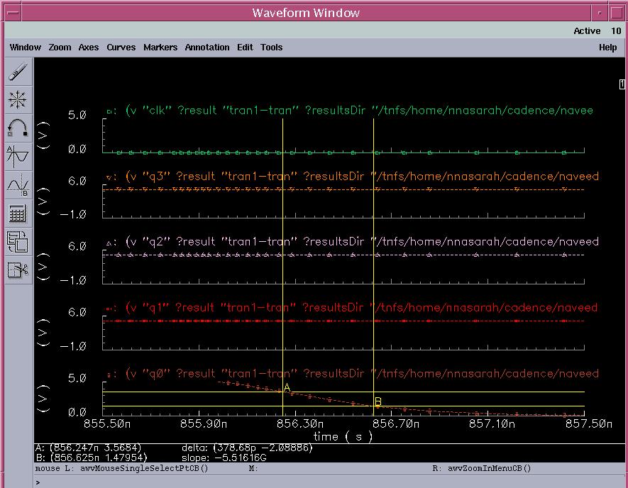
11 Figure 14: Output of LVS to show that the netlists match This is the most important part of the entire project and for this reason it is imperative the netlist match, if they do not then the error should be sought, if possible, and corrected. In this case, they are identical. The next few processes were to estimate the rise and fall times of each individual section of the project. 11
12 Figure 15: Schematic Waveform Output with rise time (30% - 70%) The estimated rise time is psec 12
 The estimated fall time is 147.")
13 Figure 16: Schematic Waveform Output with fall time (70% - 30%) The estimated fall time is psec 13
14 Figure 17: Extracted Waveform Output with rise time (30% - 70%) The estimated rise time is psec 14
 = 8837.37 µm 2.")
15 Figure 18: Schematic Waveform Output with fall time (70% - 30%) The estimated fall time is psec CONCLUSION The end results for each section are designated in their specific section and the end Area of this layout was shown to be (69.15 µm * µm) = µm 2. This project seemed very straightforward and was not very difficult except for when encountering the layout portion of this lab. The laboratory process was a simple on to design once the information of each different design was reviewed (T Flip-Flop, J-K Flip-Flop, and the selected D Flip-Flop). This project was really in depth and was considered to be a culmination of all the labs that were performed for this class. I really enjoyed the process of this project process except trying to debug the layout portion of the lab. 15
16 Report 2 Contents: 1) Abstract 2) Introduction 3) 1-bit cell development a. schematic b. layout 4) 4-bit cell development a. schematic b. layout 5) Results a. 1-bit b. 4-bit, c. LVS matching 6) Measurements and plots a. Rise time, Fall time and propagation delay b. Effect of loading 7) Summary /Conclusion 16
17 Abstract: This project involves the design and simulation of a 4-bit counter. This was accomplished in two steps. In the first step a Toggle master-slave flip-flop was designed and verified on the schematic as well as the layout level using the netlist generated by Spectre Simulations. In the second step, simulation and layout of the 4-bit counter was performed. The design was simulated under no load and 4-load conditions to validate the functionality and to estimate the delay involved in each cell. Introduction: Counters are designed using flip-flops in order to have knowledge of the previous state to decide on the next state depending on the inputs applied. Counters can be classified as synchronous and asynchronous counters based on the application of clock to the flip-flops. A synchronous counter is clocked by a single clock for all the stages and the output for each stage changes at the same time. In an asynchronous the output from the previous stage is given as the clock for the next stage so that the output ripples across each stage to reach the final count. I chose to implement an asynchronous counter in this project to test the propagation delay involved in rippling the output across the different stages of the 4-bit counter. The counter was designed for use of few gates and to provide an output that is free of glitches. A binary counter can be realized using T-FFs by counting the number of toggles in the previous stage. The T input of each flip-flop is set to 1 to produce a toggle at each cycle of the clock input. For each two toggles of the first cell, a toggle is produced in the second cell, and so on down to the fourth cell. This produces a binary number equal to the number of cycles of the input clock signal. This device is sometimes called a "ripple through" counter. Using a Master-slave configuration isolates the output from any glitches resulting from any changes happening in the input signal. The master-slave flip-flop is essentially two back-to-back JK flip-flops, but the feedback is to both to the master FF and the slave FF. In this configuration, the master FF sees the input when the clock is high and the output of the first stage holds the input for the next stage. During the clock low, the slave circuit is enabled to track the change in the input by using the output of the master FF. Thus the master-slave configuration eliminates any sharp change of state within a clock cycle and the FF is free of oscillations. Implementation: The Counter was implemented using the Toggle Flip-flops using 3 levels of hierarchy as: Implementation of 2 and 3 input NAND gates Implementation of T-FF using the basic cells developed Implementation of 4-bit Counter using the T-FFs 17

18 The following steps were performed for each cell that was developed to realize the counter. Creation of schematic Symbol creation Netlist generation and simulation of the schematic using Spectre Manual Layout creation Extraction of the layout LVS check and post-layout simulation using Spectre 1-bit Cell: The schematic of the Toggle FF realized using gates is shown below. The FF has 2 stages i.e. the master and the slave stage. The FF requires a clock and an input which when always equal to 1 results in the constant toggling of the output Q and its inverse Q_inv. This schematic was realized and the functionality was tested using the netlist simulation in spectre. Then the symbol for the single slice of the counter was generated and the manual layout was drawn. Layout: The layouts of the individual NAND gates were drawn and the functionality was verified. The size used for the n-mos and the p-mos used for the initial cells were retained in order to maintain consistency across all the cells. NMOS: L = 0.6 µm and W = 4.5 µm PMOS : L = 0.6 µm and W = 1.5 µm The size of a standard 2 input NAND gate was µm x 13.2 µm ( µm 2 ) The layout shows that the individual NAND gates are placed side by side to reduce the layout area and for ease of interconnections. 18

19 The layout structure is 3-IP NAND 3-IP NAND 2-IP NAND - 2-IP NAND INVERTER -2-IP NAND -2-IP NAND -2-IP NAND -2-IP NAND. The layout occupies an area of µm 2 (86.25µm by 28.65µm). The input leads are seen entering in the left side and the outputs of Q and Q_inv are seen leaving at the right side. Thus it is a simple configuration to fabricate. 4-bit Counter: The schematic of the 4-bit Counter realized using 1-bit Counter cells is shown below. There are 4 FFs required for the counter and the enable input of 1 is given to all the FFs. The input clock is required for the first stage only and the output from the Q_inv of the previous stage is used as the clock for the subsequent stages. This schematic was realized and the functionality was tested using the netlist simulation in spectre. 19
20 Then the symbol for the single slice of the counter was generated and the manual layout was drawn. Layout: The layout shows that the individual TFFs were placed on below the other to use the layout area in an effective manner and for ease of interconnections. 20
.")
21 The layout structure from the top to the bottom is TFF(Q_3 MSB) TFF(Q_2) TFF(Q_1) TFF(Q_0 LSB) The layout occupies an area of µm 2 (86.25µm by µm). The input leads are seen entering in the left side and the outputs of Q and Q_inv are seen leaving at the right side. 21


22 Simulation Results: The results of simulation for a single bit and a 4-bit counter are linked below: 1-bit Counter output waveform: Q_inv Q Enable Clock The waveforms show that the output changes at the negative edge of the clock transition. This is so because the master FF is enabled for the positive transitions and the slave responds to the negative transitions. The frequency of the output is also seen to be half that of the clock and the output toggles for every clock cycle due to the constant 1 input to the toggle FF. 4-bit Counter Waveform: Q_3 (MSB) Q_2 Q_1 Q_0 (LSB) Enable Clock 22
23 The waveforms show the operation of the 4-bit counter. The Q_0 output which is the LSB toggles for every negative transition of the clock cycle. The output of the next stage follows with toggling depending on the transition of the previous stage and the output for the 4 stages are obtained. It is seen that the counters starts counting from 1111 to 0000 as a count-down counter and then starts again from 1111, thus counting correctly. LVS Results: The result of the LVS run shows that the netlist generated from the schematic and of the layout match perfectly. Measurements: The circuit s delay plots and measurements have been included below to show the delays involved in the different stages of the counter. The rise time, fall time and the propagation delay involved for no load and load conditions have been simulated and tabulated. The rise time was calculated as the time taken by the output signal to rise from the 0% value of 0V to 70% (3.5V) of the final value. The fall time was found as the time taken by the signal to fall from 100% (5V) to 30% (1.5V) i.e. the t -70% was calculated. The propagation delay was calculated as the time taken by the output signal to ripple out for a given change in the input signal. This was measured as the time taken between the 50% change of the input signal (in this case it is the clock) and the 50% change in the output signal of the different stages in the 4-bit counter. Table showing the delay measurements: Rise Time Fall Time Propagation Delay Load Capacitance Q0 Q1 Q2 Q3 Q0 Q1 Q2 Q3 Q0 Q1 Q2 Q3 No load 296p 309p 311p 1.08n 618p 618p 618p 1.7n 556p 2.1n 3.6n 5.2n 1pF 4.02n 4.9n 4.9n 4.869n 14.2n 14.7n 14.2n 14.8n 3.1n 7.87n 12.7n 17.5n 2pF 7.8n 8.6n 8.3n 7.6n 27.3n 26.5n 26.6n 26.4n 5.5n 13.5n 21.5n 29.5n 5pF 15.6n 18.6n 17.9n 18n 64.8n 66n 64.5n 66n 10.4n 27.5n 44.6n 62n The plots of propagation delay for various load conditions: 23
24 Delay vs Load Capacitance (Q0) Delay vs Load Capacitance (Q1) Propagation Delay in ns Load Capacitance in pf Propagation Delay in ns Load Capacitance in pf Delay vs Load Capacitance (Q2) Delay vs Load Capacitance (Q3) Propagation Delay in ns Load Capacitance in pf Propagation Delay in ns Load Capacitance in pf These measurements show that the delay increases with the increase in the load capacitance value and also illustrates the ripple effect wherein for the output for the last stage to be reflected, it requires the output from the previous stages to ripple out and reach the last stage. This leads to more delay for the output to reach the last stage when compared to the previous stages. Conclusion: Any error that was generated during the DRC or LVS check was corrected and the 4-bit Counter s functionality has been validated and it works correctly. The layout generated occupies less space and the delays involved were measured. The gds file required for fabrication of this design would be extracted. Thus this project has given a good introduction to the phases involved in designing a circuit for a chip. This counter finds it application in almost all electronic appliances which involves a timer namely in microwave ovens, washing machine etc. Report 2 Introduction 24


25 This project was assigned to gain a better understanding VLSI layout. The requirements are to design and test a four bit counter. We are allowed total design freedom meaning there are no restrictions on how the counter is to be constructed. We are to choice a design and construct the circuit schematic in Cadence. Then run simulations on the schematic to test for proper execution. Next we are to layout the design making sure we meet all design rules. Finally we do post layout simulation and compare the results to the pre layout simulations. The design will use the logic devices that we created from previous labs. Once the counter works properly we are to do more in-depth testing of the propagation delay and the rise time and fall time of the counter. Theory & Design I choose to use a D flip flop for the project. D flip flops are latches that hold on to a value from the previous state until they are signaled to change. When the clock goes high, what ever value D is gets transferred to Q. When the clock goes low Q will not change. Basically Q stores the value of D until the clock goes high again. While doing research on counters on the internet, every counter I found was based on a J K flip flop. I wanted to do something different so I kept searching and soon found a simple example of a D flip flop and how to connect the flip flop into a counter. The schematic I found only used 4 flip flops which are a lot less then the other flip flop designs that I encountered. I thought if I could make the counter from such a simple D flip flop that I would end up using less area then other students designs. I liked how the design only used NAND gates whereas other designs also used NOR gates. The simple schematic can be seen in Figure 1. Figure 1 First Failed Attempt After drawing the schematics for this simple design, I tested the circuit by simulating it in Cadence. The simulation showed that the counter did not work correctly. I finally realized that maybe this was not the best design for a D flip flop. Searching the internet again, I soon found a better design that still only used NAND gates except this time there were 8 NAND gates and one inverter. Figure 2 Final Design Schematic Figure 2 shows the schematic for the more complex but effective D flip flop. This flip flop is a negative edge trigger, which means that Q will change only on the falling edge of the clock cycle. Several D flip flops can be connected together to form a counter. 25
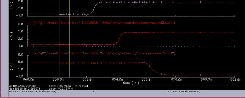
26 When D flip flops are connected as shown in Figure 3 they form what is called an asynchronous ripple counter. This is the type of counter I will be using for the project. I constructed the flip flop with 8 two input NAND gates and 1 inverter. I used the symbols I created from the previous labs to construct the schematic. I did not change any of the values for NMOS or PMOS; they are the same as they were in the lab, which is 3u/0.6u for NMOS and 7.5u/0.6u for PMOS. The schematic can be seen in Figure 4. The color has been modified to help the devices standout. Figure 4 Schematic of D flip flop Next I simulated this circuit to make sure that it works correctly. The simulation in Figure 5 shows the correct operation of a negative edge triggered D flip flop. I made the simulation pulse the D input when the clock was low to demonstrate that Q does not 26


27 change until the next clock pulse, this explains the jump of the red graph in Figure 5. Figure 5 Simulation of D flip flop Next I created a symbol for the D flip flop and began constructing the 4-bit counter. The symbol can be seen in Figure 6 and the schematic for the counter can be seen in Figure 7. Figure 6 Symbol of D flip flop 27

28 Figure 7 Schematic of 4 bit counter using D flip flops When I finished the schematic of the counter I simulated it to make sure that it did indeed count correctly. The simulation can be seen in Figure 8. A close up of the counter simulation can be seen in Figure 9. I turned the counter into a symbol as well that is shown in Figure 10. Figure 8 Simulation of Counter Schematic 28


29 Figure 9 Close up of Counter Simulation Figure 10 Counter Symbol 29


30 Layout After simulating the counter to make sure it works properly, I began creating the layout for the D flip flop. I placed the 8 NAND gates as strategically as I could to minimize the area. The gates and wires are squeezed as tightly as allowed by the design rules. I periodically had to go back and fix areas that were to close after running the Design Rule Check in Cadence. I enjoyed how Cadence allowed you to change a single gate and it would propagate through the design. This made the layout a little easier because I did not have to change all 8 NAND gates. Although, I did end up making the design harder on my self because I did not realize that I could use metal 3. This should make my layouts more impressive since I only used two types of metal. The layout for the D flip flop can be seen in Figure 11. The inputs and outputs are visible in the image. Once I had the layout for the D flip flop I just copied it 4 times into the layout for the counter. I arranged the D flip flops in a way that minimizes the amount of metal needed to connect them. The layout of the 4-bit counter can be seen in Figure 12. Figure 11 Layout of the D flip flop Figure 12 Layout of the 4 bit counter 30


31 There is only one input to the 4-bit counter, which is the left most metal contact in Figure 12 and this is for the clock signal. There are 4 outputs, one for each bit in the counter; they can be seen as the 4 highest metal contacts in Figure 12. The outputs are from left to right as follows; bit zero, bit one, bit two, and bit three. Where bit zero is the least significant bit and bit three is the most significant bit. The layout design for the counter only uses an area of 15,371 µm 2. Post Layout Simulations After completing the layout, I extracted the parasitic capacitances and preformed the same simulations as before, only this time the capacitances are taken into consideration. I also calculated the rise, fall, and delay times for the counter. Figure 13 shows the extracted layout. The correct performance of the counter can be seen from the post simulation graph in Figure 14. Figure 13 Extracted layout of counter Figure 14 Post simulation of 4 bit counter, notice the delay 31

32 A close up of the post simulation can be seen in Figure 15 it shows the delay slope in more detail. Figure 15 Close up to show delay in counter layout The following table details the rise and fall times for all of the outputs of the counter. These measurements are based on the method. Bit value Rise time Fall time Bit ps ps Bit ps ps Bit ps ps Bit ps ps Table 1 Detailing rise and fall times for the outputs I also measured the delay of different capacitive loads. I took several measurements then found where the delay values seemed to change rapidly and I took more concentrated values at that point, a graph of the delay values I found can be seen in Figure 16. The 32
33 graph shows that as the capacitive load decrease the delay will decrease. The delay seems to level out around 4 nanoseconds. Delay vs capacitance Pico Farad 40 Delay vs capacitance Delay nano seconds Figure 16 Delay of various capacitive loads Conclusions This project met its goals in that I am now a more proficient user of Cadence layout tools. I now understand more about digital logic layout and digital devices. I designed a working 4-bit counter from the ground up and proved that it worked with simulations. I encountered several problems such as a design that does not work, and having to relocate different parts of the layout because they did not meet the design rules. I have since learned to check the DRC more often. Report 3 33
34 CONTENTS ABSTRACT 1. Introduction 1.1 Project overview 1.2 JK Master Slave Flip Flop 1.3 Designing of a 4- bit Counter 1.4 Standard Height cell Format 2. Design and Implementation 2.1 Schematic of 1 bit slice 2.2 Design of 4 bit slice 3. Results SUMMARY 34
35 ABSTRACT This project involves the design and the simulation of a 4 bit counter. In the first part of the project, a one bit slice of a flip flop is drawn manually and then a schematic of JK Master-slave flip flop was designed. A layout was designed using Virtuoso and in all the cases the layout was verified using Spectre Simulation. In the second part, a 4 bit counter was designed using the 1 bit slice of the counter. It is simulated under no load, and by including some capacitances to validate its functionality and to calculate the rise time, fall time and delays. 1. INTRODUCTION 1.1 Project Overview: In this project, a standard cell design approach was used to generate the layout of Application Specific Integrated Circuit (ASIC). All the guidelines and design rules are followed in designing the layout. Firstly, a 1 bit slice of JK Flip Flop schematic was obtained and then the layout of JK Master-Slave Flip Flop was generated using Prolific and simulated using Spectre. The widths of the NFETS and PFETS were kept unchanged. 35
36 Secondly, a cell layout of 4 bit Binary Counter was generated and simulated. The schematic of the 4 bit counter was designed and it is replicated for 4 bits and the final layout was designed and simulated using Pre-Spectre and Post-Spectre simulation. A binary counter can be constructed from J-K flip flops by connecting the clock to the next counter inverted output. The J and K inputs of each flip flop are connected together to form a T flip flop to produce a toggle at each cycle of the clock input. For each two toggles of the first cell, a toggle is produced in the second cell and so on till the fourth cell. Thus a 1-bit slice of a JK flip flop is implemented and then it is extended to design a 4 bit binary counter. 1.2 JK Master Slave Flip Flop: The J-K flip-flop is perhaps the most widely used type of flip-flop. Its function is identical to that of the S-R flip flop in the SET, RESET and HOLD conditions of operation. The difference is that the J-K flip-flop does not have any invalid states. In other words, the JK flip-flop is an SRFF with some additional gating logic on the inputs which serve to overcome the SR=11 prohibited state in the SRFF. A simple JKFF is illustrated below 36
37 One way of overcoming the problem with oscillation that occurs with a JK Flip-when J=K=1 is to use a so-called master-slave flip-flop which is illustrated below. The master-slave flip-flop is essentially two back-to-back JKFFs and the feedback from this device is fed back both to the master FF and the slave FF. Also the NAND gates may have any number of inputs. The behavior of JK flip flop is completely predictable. Any input to the master-slave flip-flop at J and K is first seen by the master FF part of the circuit while CLK is High (=1). This behavior effectively locks the input into the master FF. An important feature here is that the complement of the CLK pulse is fed to the slave FF. Therefore the outputs from the master FF are only seen by the slave FF when CLK is Low (=0). Therefore on the High-to-Low CLK transition the outputs of the master are fed through the slave FF. This means that the at most one change of state can occur when J=K=1 and so oscillation between the states Q=0 and Q=1 at successive CLK pulses does not occur. 1.3 T Flip Flop: Firstly, a JK flip flop was implemented in this project and the by shorting J and K a T flip flop was designed. The T input is the CLK input for other types of flip flops. The T or "toggle" flip-flop changes its output on each clock edge, giving an output which is half the frequency of the signal to the T input. 37
38 It is useful for constructing binary counters, frequency dividers, and general binary addition devices. Counters can be designed in many ways. They can be broadly classified into Synchronous and Asynchronous counters. Asynchronous counters do not have a common clock that controls all the flip-flop stages. The control clock is input to the first stage, or the LSB stage of the counter. The clock for each stage subsequent is obtained from the flip-flop from the prior stage. This type of counter is also known as Ripple Counter. 1.4 Standard Height Cell Format: The standard-height in this design is 96-lambda. The W/L of pfet is 15/2, and nfet is 15/6. The following rules for standard-height cells were followed. All the standard cells share the same height. The wells must be as indicated on the sides of the cell. However, the center of the design can have the NMOS and PMOS transistor in any configuration so long as no DRC errors occur in the spacing. The vdd and gnd supply must be labeled as vdd! and gnd!. The final cell must have the left-bottom corner positioned at the left-bottom corner of the grid. 38
39 2. DESIGN AND IMPLEMENTATION 2.1 Schematic of 1 bit Slice: A 1-bit slice which is a T flip flop was implemented. First, the 1-bit slice schematic was built using Cadence Composer and pre-layout simulations using Spectre were performed. A manual layout from the Composer schematic that conforms to the standard-height format was produced using Virtuoso. Lastly, a manual layout from the Composer schematic that conforms to a bit-slice format was produced by Virtuoso. After the layouts were generated in these cases, DRC checks and post-layout simulations were performed. 2.2 Design of a 4 bit Slice: In this design, 4- bit slice schematic was implemented from 1 bit slice of the counter using Cadence composer, then a layout is drawn using Virtuoso and post layout simulations are performed. Thus the delay for each bit is calculated. The LVS was 39
40 checked for correctness of all the connections at the input and output. The waveforms are obtained for the counter. Steps involved in designing a 4 bit counter: A schematic is designed. All the gates and inverter are imported from other libraries. A pre-layout spectre simulation is performed. A layout is generated using Virtuoso based on the schematic. The extracted view and LVS results are obtained. The Post-layout spectre simulation gives the results. 3. RESULTS The input value T is kept all time high. As the value is high at the negative edge clock, the output Q will toggle. The layout and simulation should be performed thoroughly for better results. Also a graph, delay Vs Capacitance is plotted. Length X Width : 328um X um Area Rise Time (ns) Fall Time (ns) : (um) : 0.6ns : 1.2ns 40
41 SUMMARY This project is to design a 4 bit binary counter in chip level. The layout obtained from the prolific tools is accurate. The DRC errors have to be eliminated during the process of plotting and the layout should be compact in order to decrease the area of the layout while implementing it on a chip. 41
42 References: 1. Digital Integrated Circuits Ken Martin 2. Digital Design M. Morris Mano. 42
43 Report 4 Contents Introduction..3 Project Overview..4 T- Flip Flop Schematic...5 T-Flip Flop layout. 6 Post Spectra simulation of Flip Flop. 7 Schematic 4 Bit Counter 8 Layout 4 Bit Counter.9 Rise Time & Fall Time..12 Delay Vs Load Capacitance...14 Summary References.15 43
44 Introduction A Sequential network is a digital system where the output is determined by both the present input and the result of a previous event. A counter is a device which implements the sequential logic. The Counter is a very critical and integral part of all digital systems, especially as system complexity increases. The counter can be designed in many ways, in general a modulo N counter has N states, labeled 0 thro N-1. It Resets to 0 after the Nth pulse. For a binary counter with K flip-flops N=2k Counters have many applications such as 1. Decade Counters that count from UP/DOWN COUNTERS that have either a steering control or two pulse input lines 3. Divide by N counters 4. Used in various devices such as ATM s, Watches etc. 44
45 Project Overview: The counter was built with the help of a T-Flip Flop, The gates used were only a 3 Input Nand Gates a 2 Input Nand gates and an inverter for realizing the design. The outputs of the Flip Flop are q and qinv. The clock is the input given to the first two Nand gates and the inverter. The T-Flip Flop was chosen for its simplicity and to avoid glitches in the output. The flip-flop was asynchronous design where the q inv output of each stage was an input to the next stage. The Layout was drawn with the help of Cadence. The LVS and post spectra simulation was performed also a load capacitance in the rage of 0.5 pf to 12 pf was added and the delay was calculated. The various Delay Vs load Capacitance delay was the plotted on an excel sheet. The graph shows each delay of Individual Bits as well as the Rise Time and Fall Time. 45

46 The T Flip Flop Composer Schematic This was the schematic used in the design of the T Flip Flop the clk input is given to the first 2 Nand gates and also the inverter. 46

47 The T Flip Flop layout The design of the flip flop in cadence, the extracted view is below 47

48 Post spectra simulation The post spectra simulation was done and the output of the flip-flop is below 48

49 Schematic of the 4 Bit Counter The Inputs CLK and T are on the left side given to the first flip-flop and output of each flip q inverted is given as an input to the next stage. The output q0 q1 q2 q3 are on the right of each flip-flop. The clock is on the first flip flop and the two J and K pins are shorted to form the T-Flip Flop. 49

50 Layout of the 4 bit counter The 4 bit counter extracted view, the VDD rail is on the left and GND rail is on the right. The output q0 q1 q2 q3 are on the right of each flip-flop. The clock is on the first flip flop and the two J and K pins are shorted to form the T-Flip Flop. 50

51 Post Spectra Simulation The LVS was performed to see if the layout is in accordance with the schematic. The net- lists matched which shows that all the nets and transistors are in order. 51

52 Post Spectra simulation- Waveform 52

53 Post Spectra simulation-rise Time Post Spectra simulation-rise Time 53

54 Post Spectra simulation- Delay 54
55 Delay Vs Load capacitance As the load capacitance is increased the delay increases and the output is shown in the graphs below. Also the rise time and fall times are shown. The curves are shown for the individual Bits q1 q2 q3 q4. Delay Vs Load Capacitance Delay q3 q2 q1 q pf.5pf.7pf 2pf 4pf 6pf 8pf 10pf Capacitance Q3-Lsb Q0-Msb 55
56 Summary and Results The 4 bit counter was designed and its working was observed. The design was kept as small as possible. The design specifications are given below. Area of Layout = 170 X 210 um 2 Delay Vs Load Capacitance.2pf.5pf.7pf 2pf 4pf 6pf 8pf 10pf q q q q Rise Time and Fall Times Rise time Fall Time q q q q Refrences: 1. Digital Integrated Circuit Design by ken Martin
57 Test Result 57
58 58
59 59
60 60
61 61
62 62
63 63
64 64
Report on 4-bit Counter design Report- 1, 2. Report on D- Flipflop. Course project for ECE533
 Report on 4-bit Counter design Report- 1, 2. Report on D- Flipflop Course project for ECE533 I. Objective: REPORT-I The objective of this project is to design a 4-bit counter and implement it into a chip
Design and Simulation of a Digital CMOS Synchronous 4-bit Up-Counter with Set and Reset
 Design and Simulation of a Digital CMOS Synchronous 4-bit Up-Counter with Set and Reset Course Number: ECE 533 Spring 2013 University of Tennessee Knoxville Instructor: Dr. Syed Kamrul Islam Prepared by
EL302 DIGITAL INTEGRATED CIRCUITS LAB #3 CMOS EDGE TRIGGERED D FLIP-FLOP. Due İLKER KALYONCU, 10043
 EL302 DIGITAL INTEGRATED CIRCUITS LAB #3 CMOS EDGE TRIGGERED D FLIP-FLOP Due 16.05. İLKER KALYONCU, 10043 1. INTRODUCTION: In this project we are going to design a CMOS positive edge triggered master-slave
IT T35 Digital system desigm y - ii /s - iii
 UNIT - III Sequential Logic I Sequential circuits: latches flip flops analysis of clocked sequential circuits state reduction and assignments Registers and Counters: Registers shift registers ripple counters
SEQUENTIAL LOGIC. Satish Chandra Assistant Professor Department of Physics P P N College, Kanpur
 SEQUENTIAL LOGIC Satish Chandra Assistant Professor Department of Physics P P N College, Kanpur www.satish0402.weebly.com OSCILLATORS Oscillators is an amplifier which derives its input from output. Oscillators
RS flip-flop using NOR gate
 RS flip-flop using NOR gate Triggering and triggering methods Triggering : Applying train of pulses, to set or reset the memory cell is known as Triggering. Triggering methods:- There are basically two
Introduction to Sequential Circuits
 Introduction to Sequential Circuits COE 202 Digital Logic Design Dr. Muhamed Mudawar King Fahd University of Petroleum and Minerals Presentation Outline Introduction to Sequential Circuits Synchronous
Chapter 4. Logic Design
 Chapter 4 Logic Design 4.1 Introduction. In previous Chapter we studied gates and combinational circuits, which made by gates (AND, OR, NOT etc.). That can be represented by circuit diagram, truth table
Experiment 8 Introduction to Latches and Flip-Flops and registers
 Experiment 8 Introduction to Latches and Flip-Flops and registers Introduction: The logic circuits that have been used until now were combinational logic circuits since the output of the device depends
Rangkaian Sekuensial. Flip-flop
 Rangkaian Sekuensial Rangkaian Sekuensial Flip-flop Combinational versus Sequential Functions Logic functions are categorized as being either combinational (sometimes referred to as combinatorial) or sequential.
YEDITEPE UNIVERSITY DEPARTMENT OF COMPUTER ENGINEERING. EXPERIMENT VIII: FLIP-FLOPS, COUNTERS 2014 Fall
 YEDITEPE UNIVERSITY DEPARTMENT OF COMPUTER ENGINEERING EXPERIMENT VIII: FLIP-FLOPS, COUNTERS 2014 Fall Objective: - Dealing with the operation of simple sequential devices. Learning invalid condition in
CS/EE 6710 Digital VLSI Design CAD Assignment #3 Due Thursday September 21 st, 5:00pm
 CS/EE 6710 Digital VLSI Design CAD Assignment #3 Due Thursday September 21 st, 5:00pm Overview: In this assignment you will design a register cell. This cell should be a single-bit edge-triggered D-type
Sequential Logic. E&CE 223 Digital Circuits and Systems (A. Kennings) Page 1
 Page 1") Sequential Logic E&CE 223 igital Circuits and Systems (A. Kennings) Page 1 Sequential Circuits Have considered only combinational circuits in which circuit outputs are determined entirely by current circuit
Sequential Logic E&CE 223 igital Circuits and Systems (A. Kennings) Page 1 Sequential Circuits Have considered only combinational circuits in which circuit outputs are determined entirely by current circuit
NH 67, Karur Trichy Highways, Puliyur C.F, Karur District UNIT-III SEQUENTIAL CIRCUITS
 NH 67, Karur Trichy Highways, Puliyur C.F, 639 114 Karur District DEPARTMENT OF ELETRONICS AND COMMUNICATION ENGINEERING COURSE NOTES SUBJECT: DIGITAL ELECTRONICS CLASS: II YEAR ECE SUBJECT CODE: EC2203
Flip-Flops. Because of this the state of the latch may keep changing in circuits with feedback as long as the clock pulse remains active.
 Flip-Flops Objectives The objectives of this lesson are to study: 1. Latches versus Flip-Flops 2. Master-Slave Flip-Flops 3. Timing Analysis of Master-Slave Flip-Flops 4. Different Types of Master-Slave
Name Of The Experiment: Sequential circuit design Latch, Flip-flop and Registers
 EEE 304 Experiment No. 07 Name Of The Experiment: Sequential circuit design Latch, Flip-flop and Registers Important: Submit your Prelab at the beginning of the lab. Prelab 1: Construct a S-R Latch and
Asynchronous (Ripple) Counters
 Counters") Circuits for counting events are frequently used in computers and other digital systems. Since a counter circuit must remember its past states, it has to possess memory. The chapter about flip-flops introduced
Circuits for counting events are frequently used in computers and other digital systems. Since a counter circuit must remember its past states, it has to possess memory. The chapter about flip-flops introduced
RS flip-flop using NOR gate
 RS flip-flop using NOR gate Triggering and triggering methods Triggering : Applying train of pulses, to set or reset the memory cell is known as Triggering. Triggering methods:- There are basically two
Logic Design. Flip Flops, Registers and Counters
 Logic Design Flip Flops, Registers and Counters Introduction Combinational circuits: value of each output depends only on the values of inputs Sequential Circuits: values of outputs depend on inputs and
DIGITAL SYSTEM FUNDAMENTALS (ECE421) DIGITAL ELECTRONICS FUNDAMENTAL (ECE422) LATCHES and FLIP-FLOPS
 DIGITAL ELECTRONICS FUNDAMENTAL (ECE422) LATCHES and FLIP-FLOPS") COURSE / CODE DIGITAL SYSTEM FUNDAMENTALS (ECE421) DIGITAL ELECTRONICS FUNDAMENTAL (ECE422) LATCHES and FLIP-FLOPS In the same way that logic gates are the building blocks of combinatorial circuits, latches
COURSE / CODE DIGITAL SYSTEM FUNDAMENTALS (ECE421) DIGITAL ELECTRONICS FUNDAMENTAL (ECE422) LATCHES and FLIP-FLOPS In the same way that logic gates are the building blocks of combinatorial circuits, latches
CHAPTER 1 LATCHES & FLIP-FLOPS
 CHAPTER 1 LATCHES & FLIP-FLOPS 1 Outcome After learning this chapter, student should be able to; Recognize the difference between latches and flipflops Analyze the operation of the flip flop Draw the output
Logic Gates, Timers, Flip-Flops & Counters. Subhasish Chandra Assistant Professor Department of Physics Institute of Forensic Science, Nagpur
 Logic Gates, Timers, Flip-Flops & Counters Subhasish Chandra Assistant Professor Department of Physics Institute of Forensic Science, Nagpur Logic Gates Transistor NOT Gate Let I C be the collector current.
FLIP-FLOPS AND RELATED DEVICES
 C H A P T E R 5 FLIP-FLOPS AND RELATED DEVICES OUTLINE 5- NAND Gate Latch 5-2 NOR Gate Latch 5-3 Troubleshooting Case Study 5-4 Digital Pulses 5-5 Clock Signals and Clocked Flip-Flops 5-6 Clocked S-R Flip-Flop
(CSC-3501) Lecture 7 (07 Feb 2008) Seung-Jong Park (Jay) CSC S.J. Park. Announcement
 Lecture 7 (07 Feb 2008) Seung-Jong Park (Jay) CSC S.J. Park. Announcement") Seung-Jong Park (Jay) http://www.csc.lsu.edu/~sjpark Computer Architecture (CSC-3501) Lecture 7 (07 Feb 2008) 1 Announcement 2 1 Combinational vs. Sequential Logic Combinational Logic Memoryless Outputs
Seung-Jong Park (Jay) http://www.csc.lsu.edu/~sjpark Computer Architecture (CSC-3501) Lecture 7 (07 Feb 2008) 1 Announcement 2 1 Combinational vs. Sequential Logic Combinational Logic Memoryless Outputs
ASYNCHRONOUS COUNTER CIRCUITS
 ASYNCHRONOUS COUNTER CIRCUITS Asynchronous counters do not have a common clock that controls all the Hipflop stages. The control clock is input into the first stage, or the LSB stage of the counter. The
MC9211 Computer Organization
 MC9211 Computer Organization Unit 2 : Combinational and Sequential Circuits Lesson2 : Sequential Circuits (KSB) (MCA) (2009-12/ODD) (2009-10/1 A&B) Coverage Lesson2 Outlines the formal procedures for the
Chapter 5 Flip-Flops and Related Devices
 Chapter 5 Flip-Flops and Related Devices Chapter 5 Objectives Selected areas covered in this chapter: Constructing/analyzing operation of latch flip-flops made from NAND or NOR gates. Differences of synchronous/asynchronous
Chapter 7 Counters and Registers
 Chapter 7 Counters and Registers Chapter 7 Objectives Selected areas covered in this chapter: Operation & characteristics of synchronous and asynchronous counters. Analyzing and evaluating various types
Module -5 Sequential Logic Design
 Module -5 Sequential Logic Design 5.1. Motivation: In digital circuit theory, sequential logic is a type of logic circuit whose output depends not only on the present value of its input signals but on
Vignana Bharathi Institute of Technology UNIT 4 DLD
 DLD UNIT IV Synchronous Sequential Circuits, Latches, Flip-flops, analysis of clocked sequential circuits, Registers, Shift registers, Ripple counters, Synchronous counters, other counters. Asynchronous
UNIT-3: SEQUENTIAL LOGIC CIRCUITS
 UNIT-3: SEQUENTIAL LOGIC CIRCUITS STRUCTURE 3. Objectives 3. Introduction 3.2 Sequential Logic Circuits 3.2. NAND Latch 3.2.2 RS Flip-Flop 3.2.3 D Flip-Flop 3.2.4 JK Flip-Flop 3.2.5 Edge Triggered RS Flip-Flop
EMT 125 Digital Electronic Principles I CHAPTER 6 : FLIP-FLOP
 EMT 125 Digital Electronic Principles I CHAPTER 6 : FLIP-FLOP 1 Chapter Overview Latches Gated Latches Edge-triggered flip-flops Master-slave flip-flops Flip-flop operating characteristics Flip-flop applications
UNIT III. Combinational Circuit- Block Diagram. Sequential Circuit- Block Diagram
 UNIT III INTRODUCTION In combinational logic circuits, the outputs at any instant of time depend only on the input signals present at that time. For a change in input, the output occurs immediately. Combinational
ELCT201: DIGITAL LOGIC DESIGN
 ELCT201: DIGITAL LOGIC DESIGN Dr. Eng. Haitham Omran, haitham.omran@guc.edu.eg Dr. Eng. Wassim Alexan, wassim.joseph@guc.edu.eg Lecture 6 Following the slides of Dr. Ahmed H. Madian ذو الحجة 1438 ه Winter
COE 202: Digital Logic Design Sequential Circuits Part 1. Dr. Ahmad Almulhem ahmadsm AT kfupm Phone: Office:
 COE 202: Digital Logic Design Sequential Circuits Part 1 Dr. Ahmad Almulhem Email: ahmadsm AT kfupm Phone: 860-7554 Office: 22-324 Objectives Sequential Circuits Memory Elements Latches Flip-Flops Combinational
Introduction. NAND Gate Latch. Digital Logic Design 1 FLIP-FLOP. Digital Logic Design 1
 2007 Introduction BK TP.HCM FLIP-FLOP So far we have seen Combinational Logic The output(s) depends only on the current values of the input variables Here we will look at Sequential Logic circuits The
Sequential Logic and Clocked Circuits
 Sequential Logic and Clocked Circuits Clock or Timing Device Input Variables State or Memory Element Combinational Logic Elements From combinational logic, we move on to sequential logic. Sequential logic
CSE Latches and Flip-flops Dr. Izadi. NOR gate property: A B Z Cross coupled NOR gates: S M S R Q M
 CSE-4523 Latches and Flip-flops Dr. Izadi NOR gate property: A B Z A B Z Cross coupled NOR gates: S M S R M R S M R S R S R M S S M R R S ' Gate R Gate S R S G R S R (t+) S G R Flip_flops:. S-R flip-flop
DIGITAL SYSTEM FUNDAMENTALS (ECE421) DIGITAL ELECTRONICS FUNDAMENTAL (ECE422) COUNTERS
 DIGITAL ELECTRONICS FUNDAMENTAL (ECE422) COUNTERS") COURSE / CODE DIGITAL SYSTEM FUNDAMENTALS (ECE421) DIGITAL ELECTRONICS FUNDAMENTAL (ECE422) COUNTERS One common requirement in digital circuits is counting, both forward and backward. Digital clocks and
COURSE / CODE DIGITAL SYSTEM FUNDAMENTALS (ECE421) DIGITAL ELECTRONICS FUNDAMENTAL (ECE422) COUNTERS One common requirement in digital circuits is counting, both forward and backward. Digital clocks and
Switching Theory And Logic Design UNIT-IV SEQUENTIAL LOGIC CIRCUITS
 Switching Theory And Logic Design UNIT-IV SEQUENTIAL LOGIC CIRCUITS Sequential circuits Classification of sequential circuits: Sequential circuits may be classified as two types. 1. Synchronous sequential
CPS311 Lecture: Sequential Circuits
 CPS311 Lecture: Sequential Circuits Last revised August 4, 2015 Objectives: 1. To introduce asynchronous and synchronous flip-flops (latches and pulsetriggered, plus asynchronous preset/clear) 2. To introduce
DESIGN AND IMPLEMENTATION OF SYNCHRONOUS 4-BIT UP COUNTER USING 180NM CMOS PROCESS TECHNOLOGY
 DESIGN AND IMPLEMENTATION OF SYNCHRONOUS 4-BIT UP COUNTER USING 180NM CMOS PROCESS TECHNOLOGY Yogita Hiremath 1, Akalpita L. Kulkarni 2, J. S. Baligar 3 1 PG Student, Dept. of ECE, Dr.AIT, Bangalore, Karnataka,
Lecture 8: Sequential Logic
 Lecture 8: Sequential Logic Last lecture discussed how we can use digital electronics to do combinatorial logic we designed circuits that gave an immediate output when presented with a given set of inputs
Counters
 Counters A counter is the most versatile and useful subsystems in the digital system. A counter driven by a clock can be used to count the number of clock cycles. Since clock pulses occur at known intervals,
Unit 11. Latches and Flip-Flops
 Unit 11 Latches and Flip-Flops 1 Combinational Circuits A combinational circuit consists of logic gates whose outputs, at any time, are determined by combining the values of the inputs. For n input variables,
ELE2120 Digital Circuits and Systems. Tutorial Note 7
 ELE2120 Digital Circuits and Systems Tutorial Note 7 Outline 1. Sequential Circuit 2. Gated SR Latch 3. Gated D-latch 4. Edge-Triggered D Flip-Flop 5. Asynchronous and Synchronous reset Sequential Circuit
Digital Logic Design Sequential Circuits. Dr. Basem ElHalawany
 Digital Logic Design Sequential Circuits Dr. Basem ElHalawany Combinational vs Sequential inputs X Combinational Circuits outputs Z A combinational circuit: At any time, outputs depends only on inputs
EKT 121/4 ELEKTRONIK DIGIT 1
 EKT 2/4 ELEKTRONIK DIGIT Kolej Universiti Kejuruteraan Utara Malaysia Sequential Logic Circuits - COUNTERS - LATCHES (review) S-R R Latch S-R R Latch Active-LOW input INPUTS OUTPUTS S R Q Q COMMENTS Q
Other Flip-Flops. Lecture 27 1
 Other Flip-Flops Other types of flip-flops can be constructed by using the D flip-flop and external logic. Two flip-flops less widely used in the design of digital systems are the JK and T flip-flops.
ECE 341. Lecture # 2
 ECE 341 Lecture # 2 Instructor: Zeshan Chishti zeshan@pdx.edu October 1, 2014 Portland State University Announcements Course website reminder: http://www.ece.pdx.edu/~zeshan/ece341.htm Homework 1: Will
MODULE 3. Combinational & Sequential logic
 MODULE 3 Combinational & Sequential logic Combinational Logic Introduction Logic circuit may be classified into two categories. Combinational logic circuits 2. Sequential logic circuits A combinational
DALHOUSIE UNIVERSITY Department of Electrical & Computer Engineering Digital Circuits - ECED 220. Experiment 4 - Latches and Flip-Flops
 DLHOUSIE UNIVERSITY Department of Electrical & Computer Engineering Digital Circuits - ECED 0 Experiment - Latches and Flip-Flops Objectives:. To implement an RS latch memory element. To implement a JK
Experiment # 9. Clock generator circuits & Counters. Digital Design LAB
 Digital Design LAB Islamic University Gaza Engineering Faculty Department of Computer Engineering Fall 2012 ECOM 2112: Digital Design LAB Eng: Ahmed M. Ayash Experiment # 9 Clock generator circuits & Counters
Chapter 5 Synchronous Sequential Logic
 Chapter 5 Synchronous Sequential Logic Chih-Tsun Huang ( 黃稚存 ) http://nthucad.cs.nthu.edu.tw/~cthuang/ Department of Computer Science National Tsing Hua University Outline Introduction Storage Elements:
Combinational vs Sequential
 Combinational vs Sequential inputs X Combinational Circuits outputs Z A combinational circuit: At any time, outputs depends only on inputs Changing inputs changes outputs No regard for previous inputs
Design of a Low Power Four-Bit Binary Counter Using Enhancement Type Mosfet
 Design of a Low Power Four-Bit Binary Counter Using Enhancement Type Mosfet Praween Sinha Department of Electronics & Communication Engineering Maharaja Agrasen Institute Of Technology, Rohini sector -22,
Logic and Computer Design Fundamentals. Chapter 7. Registers and Counters
 Logic and Computer Design Fundamentals Chapter 7 Registers and Counters Registers Register a collection of binary storage elements In theory, a register is sequential logic which can be defined by a state
D Latch (Transparent Latch)
") D Latch (Transparent Latch) -One way to eliminate the undesirable condition of the indeterminate state in the SR latch is to ensure that inputs S and R are never equal to 1 at the same time. This is done
D Latch (Transparent Latch) -One way to eliminate the undesirable condition of the indeterminate state in the SR latch is to ensure that inputs S and R are never equal to 1 at the same time. This is done
DIGITAL CIRCUIT COMBINATORIAL LOGIC
 DIGITAL CIRCUIT COMBINATORIAL LOGIC Logic levels: one zero true false high low CMOS logic levels: 1 => 0.7 V DD 0.4 V DD = noise margin 0 =< 0.3 V DD Positive logic: high = 1 = true low = 0 = false Negative
Flip Flop. S-R Flip Flop. Sequential Circuits. Block diagram. Prepared by:- Anwar Bari
 Sequential Circuits The combinational circuit does not use any memory. Hence the previous state of input does not have any effect on the present state of the circuit. But sequential circuit has memory
ESE 570 STATIC SEQUENTIAL CMOS LOGIC CELLS. Kenneth R. Laker, University of Pennsylvania, updated 25Mar15
 ESE 570 STATIC SEQUENTIAL CMOS LOGIC CELLS 1 Classes of Logic Circuits two stable op. pts. Latch level triggered. Flip-Flop edge triggered. one stable op. pt. One-shot single pulse output no stable op.
Flip-Flops and Sequential Circuit Design
 Flip-Flops and Sequential Circuit Design ECE 52 Summer 29 Reading ssignment Brown and Vranesic 7 Flip-Flops, Registers, Counters and a Simple Processor 7.5 T Flip-Flop 7.5. Configurable Flip-Flops 7.6
LATCHES & FLIP-FLOP. Chapter 7
 LATCHES & FLIP-FLOP Chapter 7 INTRODUCTION Latch and flip flops are categorized as bistable devices which have two stable states,called SET and RESET. They can retain either of this states indefinitely
Sequential Digital Design. Laboratory Manual. Experiment #7. Counters
 The Islamic University of Gaza Engineering Faculty Department of Computer Engineering Spring 2018 ECOM 2022 Khaleel I. Shaheen Sequential Digital Design Laboratory Manual Experiment #7 Counters Objectives
Counter dan Register
 Counter dan Register Introduction Circuits for counting events are frequently used in computers and other digital systems. Since a counter circuit must remember its past states, it has to possess memory.
Chapter 6. Flip-Flops and Simple Flip-Flop Applications
 Chapter 6 Flip-Flops and Simple Flip-Flop Applications Basic bistable element It is a circuit having two stable conditions (states). It can be used to store binary symbols. J. C. Huang, 2004 Digital Logic
CHAPTER 4: Logic Circuits
 CHAPTER 4: Logic Circuits II. Sequential Circuits Combinational circuits o The outputs depend only on the current input values o It uses only logic gates, decoders, multiplexers, ALUs Sequential circuits
CHAPTER 4: Logic Circuits
 CHAPTER 4: Logic Circuits II. Sequential Circuits Combinational circuits o The outputs depend only on the current input values o It uses only logic gates, decoders, multiplexers, ALUs Sequential circuits
cascading flip-flops for proper operation clock skew Hardware description languages and sequential logic
 equential logic equential circuits simple circuits with feedback latches edge-triggered flip-flops Timing methodologies cascading flip-flops for proper operation clock skew Basic registers shift registers
Chapter 3: Sequential Logic Systems
 Chapter 3: Sequential Logic Systems 1. The S-R Latch Learning Objectives: At the end of this topic you should be able to: design a Set-Reset latch based on NAND gates; complete a sequential truth table
Sequential Digital Design. Laboratory Manual. Experiment #3. Flip Flop Storage Elements
 The Islamic University of Gaza Engineering Faculty Department of Computer Engineering Spring 2018 ECOM 2022 Khaleel I. Shaheen Sequential Digital Design Laboratory Manual Experiment #3 Flip Flop Storage
Chapter. Synchronous Sequential Circuits
 Chapter 5 Synchronous Sequential Circuits Logic Circuits- Review Logic Circuits 2 Combinational Circuits Consists of logic gates whose outputs are determined from the current combination of inputs. Performs
3 Flip-Flops. The latch is a logic block that has 2 stable states (0) or (1). The RS latch can be forced to hold a 1 when the Set line is asserted.
 or (1). The RS latch can be forced to hold a 1 when the Set line is asserted.") 3 Flip-Flops Flip-flops and latches are digital memory circuits that can remain in the state in which they were set even after the input signals have been removed. This means that the circuits have a memory
3 Flip-Flops Flip-flops and latches are digital memory circuits that can remain in the state in which they were set even after the input signals have been removed. This means that the circuits have a memory
Name: Date: Suggested Reading Chapter 7, Digital Systems, Principals and Applications; Tocci
 Richland College Engineering Technology Rev. 0 B. Donham Rev. 1 (7/2003) J. Horne Rev. 2 (1/2008) J. Bradbury Digital Fundamentals CETT 1425 Lab 7 Asynchronous Ripple Counters Name: Date: Objectives: To
Sequential Circuits: Latches & Flip-Flops
 Sequential Circuits: Latches & Flip-Flops Overview Storage Elements Latches SR, JK, D, and T Characteristic Tables, Characteristic Equations, Eecution Tables, and State Diagrams Standard Symbols Flip-Flops
CPE 200L LABORATORY 3: SEQUENTIAL LOGIC CIRCUITS UNIVERSITY OF NEVADA, LAS VEGAS GOALS: BACKGROUND: SR FLIP-FLOP/LATCH
 CPE 200L LABORATORY 3: SEUENTIAL LOGIC CIRCUITS DEPARTMENT OF ELECTRICAL AND COMPUTER ENGINEERING UNIVERSITY OF NEVADA, LAS VEGAS GOALS: Learn to use Function Generator and Oscilloscope on the breadboard.
Chapter 5: Synchronous Sequential Logic
 Chapter 5: Synchronous Sequential Logic NCNU_2016_DD_5_1 Digital systems may contain memory for storing information. Combinational circuits contains no memory elements the outputs depends only on the inputs
CSE 352 Laboratory Assignment 3
 CSE 352 Laboratory Assignment 3 Introduction to Registers The objective of this lab is to introduce you to edge-trigged D-type flip-flops as well as linear feedback shift registers. Chapter 3 of the Harris&Harris
Long and Fast Up/Down Counters Pushpinder Kaur CHOUHAN 6 th Jan, 2003
 1 Introduction Long and Fast Up/Down Counters Pushpinder Kaur CHOUHAN 6 th Jan, 2003 Circuits for counting both forward and backward events are frequently used in computers and other digital systems. Digital
Chapter 9 Counters. Clock Edge Output Q 2 Q 1 Q
 hapter 9 ounters 9. Introduction ounters are devices which have a LOK input and produce n outputs. ounters consist of flip-flops connected together in specific ways such that on each clock edge the output
The outputs are formed by a combinational logic function of the inputs to the circuit or the values stored in the flip-flops (or both).
.") 1 The outputs are formed by a combinational logic function of the inputs to the circuit or the values stored in the flip-flops (or both). The value that is stored in a flip-flop when the clock pulse occurs
1 The outputs are formed by a combinational logic function of the inputs to the circuit or the values stored in the flip-flops (or both). The value that is stored in a flip-flop when the clock pulse occurs
UNIT IV. Sequential circuit
 UNIT IV Sequential circuit Introduction In the previous session, we said that the output of a combinational circuit depends solely upon the input. The implication is that combinational circuits have no
Computer Science 324 Computer Architecture Mount Holyoke College Fall Topic Notes: Sequential Circuits
 Computer Science 324 Computer Architecture Mount Holyoke College Fall 2009 opic Notes: Sequential Circuits Let s think about how life can be bad for a circuit. Edge Detection Consider this one: What is
Sequential Logic Circuits
 Sequential Logic Circuits By Dr. M. Hebaishy Digital Logic Design Ch- Rem.!) Types of Logic Circuits Combinational Logic Memoryless Outputs determined by current values of inputs Sequential Logic Has memory
Flip-Flops and Related Devices. Wen-Hung Liao, Ph.D. 4/11/2001
 Flip-Flops and Related Devices Wen-Hung Liao, Ph.D. 4/11/2001 Objectives Recognize the various IEEE/ANSI flip-flop symbols. Use state transition diagrams to describe counter operation. Use flip-flops in
More on Flip-Flops Digital Design and Computer Architecture: ARM Edition 2015 Chapter 3 <98> 98
 More on Flip-Flops Digital Design and Computer Architecture: ARM Edition 2015 Chapter 3 98 Review: Bit Storage SR latch S (set) Q R (reset) Level-sensitive SR latch S S1 C R R1 Q D C S R D latch Q
Digital Fundamentals: A Systems Approach
 Digital Fundamentals: A Systems Approach Latches, Flip-Flops, and Timers Chapter 6 Traffic Signal Control Traffic Signal Control: State Diagram Traffic Signal Control: Block Diagram Traffic Signal Control:
Project 6: Latches and flip-flops
 Project 6: Latches and flip-flops Yuan Ze University epartment of Computer Engineering and Science Copyright by Rung-Bin Lin, 1999 All rights reserved ate out: 06/5/2003 ate due: 06/25/2003 Purpose: This
SEMESTER ONE EXAMINATIONS 2002
 SEMESTER ONE EXAMINATIONS 2002 EE101 Digital Electronics Solutions Question 1. An assembly line has 3 failsafe sensors and 1 emergency shutdown switch. The Line should keep moving unless any of the following
Computer Science 324 Computer Architecture Mount Holyoke College Fall Topic Notes: Sequential Circuits
 Computer Science 324 Computer Architecture Mount Holyoke College Fall 2007 opic Notes: Sequential Circuits Let s think about how life can be bad for a circuit. Edge Detection Consider this one: What is
CHAPTER1: Digital Logic Circuits
 CS224: Computer Organization S.KHABET CHAPTER1: Digital Logic Circuits 1 Sequential Circuits Introduction Composed of a combinational circuit to which the memory elements are connected to form a feedback
Sequential Design Basics
 Sequential Design Basics Lecture 2 topics A review of devices that hold state A review of Latches A review of Flip-Flops Unit of text Set-Reset Latch/Flip-Flops/D latch/ Edge triggered D Flip-Flop 8/22/22
Today 3/8/11 Lecture 8 Sequential Logic, Clocks, and Displays
 Today 3/8/ Lecture 8 Sequential Logic, Clocks, and Displays Flip Flops and Ripple Counters One Shots and Timers LED Displays, Decoders, and Drivers Homework XXXX Reading H&H sections on sequential logic
Module for Lab #16: Basic Memory Devices
 Module for Lab #16: Basic Memory evices evision: November 14, 2004 LAB Overview This lab introduces the concept of electronic memory. Memory circuits store the voltage present on an input signal (LHV or
CHAPTER 6 COUNTERS & REGISTERS
 CHAPTER 6 COUNTERS & REGISTERS 6.1 Asynchronous Counter 6.2 Synchronous Counter 6.3 State Machine 6.4 Basic Shift Register 6.5 Serial In/Serial Out Shift Register 6.6 Serial In/Parallel Out Shift Register
Logic Design Viva Question Bank Compiled By Channveer Patil
 Logic Design Viva Question Bank Compiled By Channveer Patil Title of the Practical: Verify the truth table of logic gates AND, OR, NOT, NAND and NOR gates/ Design Basic Gates Using NAND/NOR gates. Q.1
Engr354: Digital Logic Circuits
 Engr354: igital Circuits Chapter 7 Sequential Elements r. Curtis Nelson Sequential Elements In this chapter you will learn about: circuits that can store information; Basic cells, latches, and flip-flops;
Introduction to Microprocessor & Digital Logic
 ME262 Introduction to Microprocessor & Digital Logic (Sequential Logic) Summer 2 Sequential Logic Definition The output(s) of a sequential circuit depends d on the current and past states of the inputs,
ELCT201: DIGITAL LOGIC DESIGN
 ELCT201: DIGITAL LOGIC DESIGN Dr. Eng. Haitham Omran, haitham.omran@guc.edu.eg Dr. Eng. Wassim Alexan, wassim.joseph@guc.edu.eg Lecture 7 Following the slides of Dr. Ahmed H. Madian محرم 1439 ه Winter
EEC 118 Lecture #9: Sequential Logic. Rajeevan Amirtharajah University of California, Davis Jeff Parkhurst Intel Corporation
 EEC 118 Lecture #9: Sequential Logic Rajeevan Amirtharajah University of California, Davis Jeff Parkhurst Intel Corporation Outline Review: Static CMOS Logic Finish Static CMOS transient analysis Sequential