Digital Fundamentals
|
|
|
- Grace Black
- 5 years ago
- Views:
Transcription

1 igital Fundamentals Tenth Edition Floyd Chapter 7 Modified by Yuttapong Jiraraksopakun Floyd, igital Fundamentals, 10 th 2008 Pearson Education ENE, KMUTT ed 2009
2 Summary Latches A latch is a temporary storage device that has two stable states (bistable). It is a basic form of memory. The S-R (Set-Reset) latch is the most basic type. It can be constructed from NOR gates or NAN gates. With NOR gates, the latch responds to active-high inputs; with NAN gates, it responds to active-low inputs. R S S R NOR Active-HIGH Latch NAN Active-LOW Latch
3 Latches Summary The active-high S-R latch is in a stable (latched) condition when both inputs are LOW. Assume the latch is initially RESET ( = 0) and the inputs are at their inactive level (0). To SET the latch ( = 1), a momentary HIGH signal is applied to the S input while the R remains LOW. To RESET the latch ( = 0), a momentary HIGH signal is applied to the R input while the S remains LOW. 0 R S R S Latch initially RESET Latch initially SET
4 Latches Summary The active-low S-R latch is in a stable (latched) condition when both inputs are HIGH. Assume the latch is initially RESET ( = 0) and the inputs are at their inactive level (1). To SET the latch ( = 1), a momentary LOW signal is applied to the S input while the R remains HIGH. To RESET the latch a momentary LOW is applied to the R input while S is HIGH. Never apply an active set and reset at the same time (invalid). 1 S R S 1 R Latch initially RESET Latch initially SET

5 Summary Latches R S S R NOR Active-HIGH Latch NAN Active-LOW Latch
6 Latches Summary The active-low S-R latch is available as the 74LS279A IC. It features four internal latches with two having two S inputs. To SET any of the latches, the S line is pulsed low. It is available in several packages. S-R latches are frequently used for switch debounce circuits as shown: 1 2 V CC S R S R Position 1 to 2 Position 2 to 1 (2) (3) (1) (6) (5) (11) (12) (10) (15) (14) 1S1 1S2 1R 2S 2R 3S1 3S2 3R 4S 4R 74LS279A (4) (7) (9) (13)
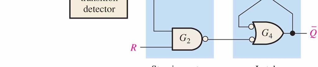
7 Gated S-R Latches Summary A gated latch is a variation on the basic latch. The gated latch has an additional input, called enable (EN) that must be HIGH in order for the latch to respond to the S and R inputs. S EN Show the output with relation to the input signals. R Assume starts LOW. Keep in mind that S and R are only active when EN is HIGH. S R EN
8 Gated Latches Summary The latch is an variation of the S-R latch but combines the S and R inputs into a single input as shown: EN EN A simple rule for the latch is: follows when the Enable is active.
9 Gated Latches Summary The truth table for the latch summarizes its operation. If EN is LOW, then there is no change in the output and it is latched. 0 1 X Inputs EN Outputs Comments RESET SET No change
10 Summary Gated Latches etermine the output for the latch, given the inputs shown. EN EN Notice that the Enable is not active during these times, so the output is latched.
11 Flip-flops Summary A flip-flop differs from a latch in the manner it changes states. A flip-flop is a clocked device, in which only the clock edge determines when a new bit is entered. The active edge can be positive or negative. C C ynamic input indicator (a) Positive edge-triggered (b) Negative edge-triggered


12 Summary S-R Flip-flops

13 Summary S-R Flip-flops

14 Summary S-R Flip-flops
15 Summary Flip-flops The truth table for a positive-edge triggered flip-flop shows an up arrow to remind you that it is sensitive to its input only on the rising edge of the clock; otherwise it is latched. The truth table for a negative-edge triggered flip-flop is identical except for the direction of the arrow. Inputs Outputs Inputs Outputs Comments Comments SET RESET SET RESET (a) Positive-edge triggered (b) Negative-edge triggered
16 Summary J-K Flip-flops The J-K flip-flop is more versatile than the flip flop. In addition to the clock input, it has two inputs, labeled J and K. When both J and K = 1, the output changes states (toggles) on the active clock edge (in this case, the rising edge). J Inputs K Outputs Comments No change RESET SET 1 1 Toggle 0 0
17 Summary J-K Flip-flops J etermine the output for the J-K flip-flop, given the inputs shown. Notice that the outputs change on the leading edge of the clock. K Set Toggle Set Latch J K
18 Summary Flip-flops A -flip-flop does not have a toggle mode like the J-K flipflop, but you can hardwire a toggle mode by connecting back to as shown. This is useful in some counters as you will see in Chapter 8. For example, if is LOW, is HIGH and the flip-flop will toggle on the next clock edge. Because the flip-flop only changes on the active edge, the output will only change once for each clock pulse. flip-flop hardwired for a toggle mode
19 Summary Asynchronous Preset and Clear Synchronous inputs are transferred in the triggering edge of the clock (for example the or J-K inputs). Most flipflops have other inputs that are asynchronous, meaning they affect the output independent of the clock. Two such inputs are normally labeled preset (PRE) and clear (CLR). These inputs are usually active LOW. A J-K flip flop with active LOW preset and CLR is shown. PRE J K CLR

20 Summary Asynchronous Preset and Clear

21 Summary PRE Flip-flops etermine the output for the J-K flip-flop, given the inputs shown. J K J K PRE CLR Set Toggle Set Reset Toggle Set Reset CLR Latch
22 Flip-flop Characteristics Propagation delay time is specified for the rising and falling outputs. It is measured between the 50% level of the clock to the 50% level of the output transition. 50% point on triggering edge Summary 50% point 50% point on LOW-to- HIGH transition of 50% point on HIGH-to- LOW transition of t PLH t PHL The typical propagation delay time for the 74AHC family (CMOS) is 4 ns. Even faster logic is available for specialized applications.
23 Flip-flop Characteristics Summary Another propagation delay time specification is the time required for an asynchronous input to cause a change in the output. Again it is measured from the 50% levels. The 74AHC family has specified delay times under 5 ns. PRE 50% point CLR 50% point 50% point 50% point t PHL t PLH
24 Flip-flop Characteristics Summary Set-up time and hold time are times required before and after the clock transition that data must be present to be reliably clocked into the flip-flop. Setup time is the minimum time for the data to be present before the clock. Set-up time, t s Hold time is the minimum time for the data to remain after the clock. Hold time, t H
25 Flip-flop Characteristics Summary Other specifications include maximum clock frequency, minimum pulse widths for various inputs, and power dissipation. The power dissipation is the product of the supply voltage and the average current required. A useful comparison between logic families is the speed-power product which uses two of the specifications discussed: the average propagation delay and the average power dissipation. The unit is energy. What is the speed-power product for 74AHC74A? Use the data from Table 7-5 to determine the answer. From Table 7-5, the average propagation delay is 4.6 ns. The quiescent power dissipated is 1.1 mw. Therefore, the speed-power product is 5 pj
26 Summary Flip-flop Applications Principal flip-flop applications are for temporary data storage, as frequency dividers, and in counters (which are covered in detail in Chapter 8). C C R Output lines 0 1 R Typically, for data storage applications, a group of flip-flops are connected to parallel data lines and clocked together. ata is stored until the next clock pulse. Parallel data input lines Clock C R C 2 3 Clear R
27 Flip-flop Applications Summary For frequency division, it is simple to use a flip-flop in the toggle mode or to chain a series of toggle flip flops to continue to divide by two. HIGH HIGH One flip-flop will divide f in by 2, two flip-flops will divide f in by 4 (and so on). A side benefit of frequency division is that the output has an exact 50% duty cycle. f in f in J A K J B K f out Waveforms: f out
28 Homework 10 Chapter 7 (5, 8, 16, 17, 25)
PGT104 Digital Electronics. PGT104 Digital Electronics
 1 Part 5 Latches, Flip-flop and Timers isclaimer: Most of the contents (if not all) are extracted from resources available for igital Fundamentals 10 th Edition 2 Latches A latch is a temporary storage
Digital Fundamentals 11/2/2017. Summary. Summary. Floyd. Chapter 7. Latches
 igital Fundamentals Tenth Edition Floyd hapter 7 2009 Pearson Education, Upper 2008 Pearson Saddle iver, Education N 07458. All ights eserved A latch is a temporary storage device that has two stable states
Review of digital electronics. Storage units Sequential circuits Counters Shifters
 Review of digital electronics Storage units Sequential circuits ounters Shifters ounting in Binary A counter can form the same pattern of 0 s and 1 s with logic levels. The first stage in the counter represents
CHW 261: Logic Design
 CHW 26: Logic Design Instructors: Prof. Hala Zayed Dr. Ahmed Shalaby http://www.bu.edu.eg/staff/halazayed4 http://bu.edu.eg/staff/ahmedshalaby4# Slide Digital Fundamentals CHAPTER 7 Latches, Flip-Flops
Digital Fundamentals: A Systems Approach
 Digital Fundamentals: A Systems Approach Latches, Flip-Flops, and Timers Chapter 6 Traffic Signal Control Traffic Signal Control: State Diagram Traffic Signal Control: Block Diagram Traffic Signal Control:
LATCHES & FLIP-FLOP. Chapter 7
 LATCHES & FLIP-FLOP Chapter 7 INTRODUCTION Latch and flip flops are categorized as bistable devices which have two stable states,called SET and RESET. They can retain either of this states indefinitely
Digital Circuits ECS 371
 igital Circuits ECS 371 r. Prapun Suksompong prapun@siit.tu.ac.th Lecture 17 Office Hours: BK 3601-7 Monday 9:00-10:30, 1:30-3:30 Tuesday 10:30-11:30 1 Announcement Reading Assignment: Chapter 7: 7-1,
Introduction. NAND Gate Latch. Digital Logic Design 1 FLIP-FLOP. Digital Logic Design 1
 2007 Introduction BK TP.HCM FLIP-FLOP So far we have seen Combinational Logic The output(s) depends only on the current values of the input variables Here we will look at Sequential Logic circuits The
PRE J. Figure 25.1a J-K flip-flop with Asynchronous Preset and Clear inputs
 Asynchronous Preset and Clear Inputs The S-R, J-K and D inputs are known as synchronous inputs because the outputs change when appropriate input values are applied at the inputs and a clock signal is applied
Flip-Flops. Because of this the state of the latch may keep changing in circuits with feedback as long as the clock pulse remains active.
 Flip-Flops Objectives The objectives of this lesson are to study: 1. Latches versus Flip-Flops 2. Master-Slave Flip-Flops 3. Timing Analysis of Master-Slave Flip-Flops 4. Different Types of Master-Slave
Unit 11. Latches and Flip-Flops
 Unit 11 Latches and Flip-Flops 1 Combinational Circuits A combinational circuit consists of logic gates whose outputs, at any time, are determined by combining the values of the inputs. For n input variables,
Name Of The Experiment: Sequential circuit design Latch, Flip-flop and Registers
 EEE 304 Experiment No. 07 Name Of The Experiment: Sequential circuit design Latch, Flip-flop and Registers Important: Submit your Prelab at the beginning of the lab. Prelab 1: Construct a S-R Latch and
EMT 125 Digital Electronic Principles I CHAPTER 6 : FLIP-FLOP
 EMT 125 Digital Electronic Principles I CHAPTER 6 : FLIP-FLOP 1 Chapter Overview Latches Gated Latches Edge-triggered flip-flops Master-slave flip-flops Flip-flop operating characteristics Flip-flop applications
Chapter 6. Flip-Flops and Simple Flip-Flop Applications
 Chapter 6 Flip-Flops and Simple Flip-Flop Applications Basic bistable element It is a circuit having two stable conditions (states). It can be used to store binary symbols. J. C. Huang, 2004 Digital Logic
INTRODUCTION TO SEQUENTIAL CIRCUITS
 NOTE: Explanation Refer Class Notes Digital Circuits(15EECC203) INTRODUCTION TO SEQUENTIAL CIRCUITS by Nagaraj Vannal, Asst.Professor, School of Electronics Engineering, K.L.E. Technological University,
Engr354: Digital Logic Circuits
 Engr354: igital Circuits Chapter 7 Sequential Elements r. Curtis Nelson Sequential Elements In this chapter you will learn about: circuits that can store information; Basic cells, latches, and flip-flops;
FLIP-FLOPS AND RELATED DEVICES
 C H A P T E R 5 FLIP-FLOPS AND RELATED DEVICES OUTLINE 5- NAND Gate Latch 5-2 NOR Gate Latch 5-3 Troubleshooting Case Study 5-4 Digital Pulses 5-5 Clock Signals and Clocked Flip-Flops 5-6 Clocked S-R Flip-Flop
3 Flip-Flops. The latch is a logic block that has 2 stable states (0) or (1). The RS latch can be forced to hold a 1 when the Set line is asserted.
 or (1). The RS latch can be forced to hold a 1 when the Set line is asserted.") 3 Flip-Flops Flip-flops and latches are digital memory circuits that can remain in the state in which they were set even after the input signals have been removed. This means that the circuits have a memory
3 Flip-Flops Flip-flops and latches are digital memory circuits that can remain in the state in which they were set even after the input signals have been removed. This means that the circuits have a memory
CHAPTER 1 LATCHES & FLIP-FLOPS
 CHAPTER 1 LATCHES & FLIP-FLOPS 1 Outcome After learning this chapter, student should be able to; Recognize the difference between latches and flipflops Analyze the operation of the flip flop Draw the output
Chapter 11 Latches and Flip-Flops
 Chapter 11 Latches and Flip-Flops SKEE1223 igital Electronics Mun im/arif/izam FKE, Universiti Teknologi Malaysia ecember 8, 2015 Types of Logic Circuits Combinational logic: Output depends solely on the
UNIT-3: SEQUENTIAL LOGIC CIRCUITS
 UNIT-3: SEQUENTIAL LOGIC CIRCUITS STRUCTURE 3. Objectives 3. Introduction 3.2 Sequential Logic Circuits 3.2. NAND Latch 3.2.2 RS Flip-Flop 3.2.3 D Flip-Flop 3.2.4 JK Flip-Flop 3.2.5 Edge Triggered RS Flip-Flop
Chapter 5 Flip-Flops and Related Devices
 Chapter 5 Flip-Flops and Related Devices Chapter 5 Objectives Selected areas covered in this chapter: Constructing/analyzing operation of latch flip-flops made from NAND or NOR gates. Differences of synchronous/asynchronous
RS flip-flop using NOR gate
 RS flip-flop using NOR gate Triggering and triggering methods Triggering : Applying train of pulses, to set or reset the memory cell is known as Triggering. Triggering methods:- There are basically two
Lecture 8: Sequential Logic
 Lecture 8: Sequential Logic Last lecture discussed how we can use digital electronics to do combinatorial logic we designed circuits that gave an immediate output when presented with a given set of inputs
The outputs are formed by a combinational logic function of the inputs to the circuit or the values stored in the flip-flops (or both).
.") 1 The outputs are formed by a combinational logic function of the inputs to the circuit or the values stored in the flip-flops (or both). The value that is stored in a flip-flop when the clock pulse occurs
1 The outputs are formed by a combinational logic function of the inputs to the circuit or the values stored in the flip-flops (or both). The value that is stored in a flip-flop when the clock pulse occurs
(CSC-3501) Lecture 7 (07 Feb 2008) Seung-Jong Park (Jay) CSC S.J. Park. Announcement
 Lecture 7 (07 Feb 2008) Seung-Jong Park (Jay) CSC S.J. Park. Announcement") Seung-Jong Park (Jay) http://www.csc.lsu.edu/~sjpark Computer Architecture (CSC-3501) Lecture 7 (07 Feb 2008) 1 Announcement 2 1 Combinational vs. Sequential Logic Combinational Logic Memoryless Outputs
Seung-Jong Park (Jay) http://www.csc.lsu.edu/~sjpark Computer Architecture (CSC-3501) Lecture 7 (07 Feb 2008) 1 Announcement 2 1 Combinational vs. Sequential Logic Combinational Logic Memoryless Outputs
Sequential Logic. E&CE 223 Digital Circuits and Systems (A. Kennings) Page 1
 Page 1") Sequential Logic E&CE 223 igital Circuits and Systems (A. Kennings) Page 1 Sequential Circuits Have considered only combinational circuits in which circuit outputs are determined entirely by current circuit
Sequential Logic E&CE 223 igital Circuits and Systems (A. Kennings) Page 1 Sequential Circuits Have considered only combinational circuits in which circuit outputs are determined entirely by current circuit
ASYNCHRONOUS COUNTER CIRCUITS
 ASYNCHRONOUS COUNTER CIRCUITS Asynchronous counters do not have a common clock that controls all the Hipflop stages. The control clock is input into the first stage, or the LSB stage of the counter. The
The NOR latch is similar to the NAND latch
 5-2 NOR Gate Latch The NOR latch is similar to the NAND latch except that the Q and Q outputs are reversed. The set and clear inputs are active high, that is, the output will change when the input is pulsed
RS flip-flop using NOR gate
 RS flip-flop using NOR gate Triggering and triggering methods Triggering : Applying train of pulses, to set or reset the memory cell is known as Triggering. Triggering methods:- There are basically two
D Latch (Transparent Latch)
") D Latch (Transparent Latch) -One way to eliminate the undesirable condition of the indeterminate state in the SR latch is to ensure that inputs S and R are never equal to 1 at the same time. This is done
D Latch (Transparent Latch) -One way to eliminate the undesirable condition of the indeterminate state in the SR latch is to ensure that inputs S and R are never equal to 1 at the same time. This is done
Experiment 8 Introduction to Latches and Flip-Flops and registers
 Experiment 8 Introduction to Latches and Flip-Flops and registers Introduction: The logic circuits that have been used until now were combinational logic circuits since the output of the device depends
Synchronous Sequential Logic
 Synchronous Sequential Logic -A Sequential Circuit consists of a combinational circuit to which storage elements are connected to form a feedback path. The storage elements are devices capable of storing
CSE115: Digital Design Lecture 23: Latches & Flip-Flops
 Faculty of Engineering CSE115: Digital Design Lecture 23: Latches & Flip-Flops Sections 7.1-7.2 Suggested Reading A Generic Digital Processor Building Blocks for Digital Architectures INPUT - OUTPUT Interconnect:
EKT 121/4 ELEKTRONIK DIGIT 1
 EKT 121/4 ELEKTRONIK DIGIT 1 Kolej Universiti Kejuruteraan Utara Malaysia Bistable Storage Devices and Related Devices Introduction Latches and flip-flops are the basic single-bit memory elements used
Logic and Computer Design Fundamentals. Chapter 7. Registers and Counters
 Logic and Computer Design Fundamentals Chapter 7 Registers and Counters Registers Register a collection of binary storage elements In theory, a register is sequential logic which can be defined by a state
EET2411 DIGITAL ELECTRONICS
 5-8 Clocked D Flip-FlopFlop One data input. The output changes to the value of the input at either the positive going or negative going clock trigger. May be implemented with a J-K FF by tying the J input
More on Flip-Flops Digital Design and Computer Architecture: ARM Edition 2015 Chapter 3 <98> 98
 More on Flip-Flops Digital Design and Computer Architecture: ARM Edition 2015 Chapter 3 98 Review: Bit Storage SR latch S (set) Q R (reset) Level-sensitive SR latch S S1 C R R1 Q D C S R D latch Q
Sequential Design Basics
 Sequential Design Basics Lecture 2 topics A review of devices that hold state A review of Latches A review of Flip-Flops Unit of text Set-Reset Latch/Flip-Flops/D latch/ Edge triggered D Flip-Flop 8/22/22
Rangkaian Sekuensial. Flip-flop
 Rangkaian Sekuensial Rangkaian Sekuensial Flip-flop Combinational versus Sequential Functions Logic functions are categorized as being either combinational (sometimes referred to as combinatorial) or sequential.
Asynchronous (Ripple) Counters
 Counters") Circuits for counting events are frequently used in computers and other digital systems. Since a counter circuit must remember its past states, it has to possess memory. The chapter about flip-flops introduced
Circuits for counting events are frequently used in computers and other digital systems. Since a counter circuit must remember its past states, it has to possess memory. The chapter about flip-flops introduced
DIGITAL ELECTRONICS MCQs
 DIGITAL ELECTRONICS MCQs 1. A 8-bit serial in / parallel out shift register contains the value 8, clock signal(s) will be required to shift the value completely out of the register. A. 1 B. 2 C. 4 D. 8
EKT 121/4 ELEKTRONIK DIGIT 1
 EKT 2/4 ELEKTRONIK DIGIT Kolej Universiti Kejuruteraan Utara Malaysia Sequential Logic Circuits - COUNTERS - LATCHES (review) S-R R Latch S-R R Latch Active-LOW input INPUTS OUTPUTS S R Q Q COMMENTS Q
Digital Logic Design ENEE x. Lecture 19
 Digital Logic Design ENEE 244-010x Lecture 19 Announcements Homework 8 due on Monday, 11/23. Agenda Last time: Timing Considerations (6.3) Master-Slave Flip-Flops (6.4) This time: Edge-Triggered Flip-Flops
Digital Fundamentals. Lab 5 Latches & Flip-Flops CETT Name: Date:
 Richland College School of Engineering & Technology Rev. 0 B. Donham Rev. 1 (7/2003) J. Horne Rev. 2 (1/2008) J. Bradbury Rev. 3 (7/2015) J. Bradbury Digital Fundamentals CETT 1425 Lab 5 Latches & Flip-Flops
Sequential Logic Basics
 Sequential Logic Basics Unlike Combinational Logic circuits that change state depending upon the actual signals being applied to their inputs at that time, Sequential Logic circuits have some form of inherent
Logic Design. Flip Flops, Registers and Counters
 Logic Design Flip Flops, Registers and Counters Introduction Combinational circuits: value of each output depends only on the values of inputs Sequential Circuits: values of outputs depend on inputs and
Logic Gates, Timers, Flip-Flops & Counters. Subhasish Chandra Assistant Professor Department of Physics Institute of Forensic Science, Nagpur
 Logic Gates, Timers, Flip-Flops & Counters Subhasish Chandra Assistant Professor Department of Physics Institute of Forensic Science, Nagpur Logic Gates Transistor NOT Gate Let I C be the collector current.
SEQUENTIAL LOGIC. Satish Chandra Assistant Professor Department of Physics P P N College, Kanpur
 SEQUENTIAL LOGIC Satish Chandra Assistant Professor Department of Physics P P N College, Kanpur www.satish0402.weebly.com OSCILLATORS Oscillators is an amplifier which derives its input from output. Oscillators
CHAPTER 11 LATCHES AND FLIP-FLOPS
 CHAPTER 11 1/25 LATCHES AND FLIP-FLOPS This chapter in the book includes: Objectives Study Guide 11.1 Introduction 11.2 Set-Reset Latch 11.3 Gated D Latch 11.4 Edge-Triggered D Flip-Flop 11.5 S-R Flip-Flop
5: Sequential Logic Latches & Flip-flops
 5: Sequential Logic Latches & Flip-flops Introduction Memory Elements Pulse-Triggered Latch S-R Latch Gated S-R Latch Gated D Latch Edge-Triggered Flip-flops S-R Flip-flop D Flip-flop J-K Flip-flop T Flip-flop
Chapter 2. Digital Circuits
 Chapter 2. Digital Circuits Logic gates Flip-flops FF registers IC registers Data bus Encoders/Decoders Multiplexers Troubleshooting digital circuits Most contents of this chapter were covered in 88-217
YEDITEPE UNIVERSITY DEPARTMENT OF COMPUTER ENGINEERING. EXPERIMENT VIII: FLIP-FLOPS, COUNTERS 2014 Fall
 YEDITEPE UNIVERSITY DEPARTMENT OF COMPUTER ENGINEERING EXPERIMENT VIII: FLIP-FLOPS, COUNTERS 2014 Fall Objective: - Dealing with the operation of simple sequential devices. Learning invalid condition in
Other Flip-Flops. Lecture 27 1
 Other Flip-Flops Other types of flip-flops can be constructed by using the D flip-flop and external logic. Two flip-flops less widely used in the design of digital systems are the JK and T flip-flops.
Fundamentals of Computer Systems
 Fundamentals of Computer Systems Sequential Logic Stephen A. Edwards Columbia University Summer 2016 State-Holding Elements Bistable Elements S Latch Latch Positive-Edge-Triggered Flip-Flop Flip-Flop with
ECE 341. Lecture # 2
 ECE 341 Lecture # 2 Instructor: Zeshan Chishti zeshan@pdx.edu October 1, 2014 Portland State University Announcements Course website reminder: http://www.ece.pdx.edu/~zeshan/ece341.htm Homework 1: Will
Slide 1. Flip-Flops. Cross-NOR SR flip-flop S R Q Q. hold reset set not used. Cross-NAND SR flip-flop S R Q Q. not used reset set hold 1 Q.
 Slide Flip-Flops Cross-NOR SR flip-flop Reset Set Cross-NAND SR flip-flop Reset Set S R reset set not used S R not used reset set 6.7 Digital ogic Slide 2 Clocked evel-triggered NAND SR Flip-Flop S R SR
Unit 9 Latches and Flip-Flops. Dept. of Electrical and Computer Eng., NCTU 1
 Unit 9 Latches and Flip-Flops Dept. of Electrical and Computer Eng., NCTU 1 9.1 Introduction Dept. of Electrical and Computer Eng., NCTU 2 What is the characteristic of sequential circuits in contrast
EEE2135 Digital Logic Design Chapter 6. Latches/Flip-Flops and Registers/Counters 서강대학교 전자공학과
 EEE235 Digital Logic Design Chapter 6. Latches/Flip-Flops and Registers/Counters 서강대학교 전자공학과 . Delay and Latches ) Signal Storage a. as voltage level static memory b. as charges dynamic memory 2) Delays
cascading flip-flops for proper operation clock skew Hardware description languages and sequential logic
 equential logic equential circuits simple circuits with feedback latches edge-triggered flip-flops Timing methodologies cascading flip-flops for proper operation clock skew Basic registers shift registers
Flip-Flops and Related Devices. Wen-Hung Liao, Ph.D. 4/11/2001
 Flip-Flops and Related Devices Wen-Hung Liao, Ph.D. 4/11/2001 Objectives Recognize the various IEEE/ANSI flip-flop symbols. Use state transition diagrams to describe counter operation. Use flip-flops in
Chapter 4. Logic Design
 Chapter 4 Logic Design 4.1 Introduction. In previous Chapter we studied gates and combinational circuits, which made by gates (AND, OR, NOT etc.). That can be represented by circuit diagram, truth table
Asynchronous counters
 Asynchronous counters In the previous section, we saw a circuit using one J-K flip-flop that counted backward in a two-bit binary sequence, from 11 to 10 to 01 to 00. Since it would be desirable to have
Sequential Logic and Clocked Circuits
 Sequential Logic and Clocked Circuits Clock or Timing Device Input Variables State or Memory Element Combinational Logic Elements From combinational logic, we move on to sequential logic. Sequential logic
CHAPTER 6 COUNTERS & REGISTERS
 CHAPTER 6 COUNTERS & REGISTERS 6.1 Asynchronous Counter 6.2 Synchronous Counter 6.3 State Machine 6.4 Basic Shift Register 6.5 Serial In/Serial Out Shift Register 6.6 Serial In/Parallel Out Shift Register
Vignana Bharathi Institute of Technology UNIT 4 DLD
 DLD UNIT IV Synchronous Sequential Circuits, Latches, Flip-flops, analysis of clocked sequential circuits, Registers, Shift registers, Ripple counters, Synchronous counters, other counters. Asynchronous
ELE2120 Digital Circuits and Systems. Tutorial Note 7
 ELE2120 Digital Circuits and Systems Tutorial Note 7 Outline 1. Sequential Circuit 2. Gated SR Latch 3. Gated D-latch 4. Edge-Triggered D Flip-Flop 5. Asynchronous and Synchronous reset Sequential Circuit
Topics of Discussion
 Digital Circuits II VHDL for Digital System Design Practical Considerations References: 1) Text Book: Digital Electronics, 9 th editon, by William Kleitz, published by Pearson Spring 2015 Paul I-Hai Lin,
ELCT201: DIGITAL LOGIC DESIGN
 ELCT201: DIGITAL LOGIC DESIGN Dr. Eng. Haitham Omran, haitham.omran@guc.edu.eg Dr. Eng. Wassim Alexan, wassim.joseph@guc.edu.eg Lecture 6 Following the slides of Dr. Ahmed H. Madian ذو الحجة 1438 ه Winter
Counters
 Counters A counter is the most versatile and useful subsystems in the digital system. A counter driven by a clock can be used to count the number of clock cycles. Since clock pulses occur at known intervals,
Asynchronous Counter
 Asynchronous Counter Contents: Asynchronous/Ripple Counter Propagation Delay in Ripple Counter MOD Number Synchronous/Parallel Counter 10101010101010101010101010101010101010101010101010101010101010101010101010101010
Name: Date: Suggested Reading Chapter 7, Digital Systems, Principals and Applications; Tocci
 Richland College Engineering Technology Rev. 0 B. Donham Rev. 1 (7/2003) J. Horne Rev. 2 (1/2008) J. Bradbury Digital Fundamentals CETT 1425 Lab 7 Asynchronous Ripple Counters Name: Date: Objectives: To
Basis of sequential circuits: the R-S latch
 equential logic Asynchronous sequential logic state changes occur whenever state inputs change (elements may be simple wires or delay elements) ynchronous sequential logic state changes occur in lock step
6. Sequential Logic Flip-Flops
 ection 6. equential Logic Flip-Flops Page of 5 6. equential Logic Flip-Flops ombinatorial components: their output values are computed entirely from their present input values. equential components: their
UNIT III. Combinational Circuit- Block Diagram. Sequential Circuit- Block Diagram
 UNIT III INTRODUCTION In combinational logic circuits, the outputs at any instant of time depend only on the input signals present at that time. For a change in input, the output occurs immediately. Combinational
Fundamentals of Computer Systems
 Fundamentals of Computer Systems Sequential Logic Stephen A. Edwards Columbia University Fall 2012 State-Holding Elements Bistable Elements Equivalent circuits; right is more traditional. Two stable states:
DIGITAL SYSTEM FUNDAMENTALS (ECE421) DIGITAL ELECTRONICS FUNDAMENTAL (ECE422) COUNTERS
 DIGITAL ELECTRONICS FUNDAMENTAL (ECE422) COUNTERS") COURSE / CODE DIGITAL SYSTEM FUNDAMENTALS (ECE421) DIGITAL ELECTRONICS FUNDAMENTAL (ECE422) COUNTERS One common requirement in digital circuits is counting, both forward and backward. Digital clocks and
COURSE / CODE DIGITAL SYSTEM FUNDAMENTALS (ECE421) DIGITAL ELECTRONICS FUNDAMENTAL (ECE422) COUNTERS One common requirement in digital circuits is counting, both forward and backward. Digital clocks and
Advanced Digital Logic Design EECS 303
 Advanced Digital Logic Design EECS 303 http://ziyang.eecs.northwestern.edu/eecs303/ Teacher: Robert Dick Office: L477 Tech Email: dickrp@northwestern.edu Phone: 847 467 2298 Outline Introduction Reset/set
Review of Flip-Flop. Divya Aggarwal. Student, Department of Physics and Astro-Physics, University of Delhi, New Delhi. their state.
 pp. 4-9 Krishi Sanskriti Publications http://www.krishisanskriti.org/jbaer.html Review of Flip-Flop Divya Aggarwal Student, Department of Physics and Astro-Physics, University of Delhi, New Delhi Abstract:
Topic D-type Flip-flops. Draw a timing diagram to illustrate the significance of edge
 Topic 1.3.2 -type Flip-flops. Learning Objectives: At the end of this topic you will be able to; raw a timing diagram to illustrate the significance of edge triggering; raw a timing diagram to illustrate
Digital Fundamentals: A Systems Approach
 Digital Fundamentals: A Systems Approach Counters Chapter 8 A System: Digital Clock Digital Clock: Counter Logic Diagram Digital Clock: Hours Counter & Decoders Finite State Machines Moore machine: One
L4: Sequential Building Blocks (Flip-flops, Latches and Registers)
") L4: Sequential Building Blocks (Flip-flops, Latches and Registers) Acknowledgements: Lecture material adapted from R. Katz, G. Borriello, Contemporary Logic esign (second edition), Prentice-Hall/Pearson
L4: Sequential Building Blocks (Flip-flops, Latches and Registers) Acknowledgements: Lecture material adapted from R. Katz, G. Borriello, Contemporary Logic esign (second edition), Prentice-Hall/Pearson
Sri Vidya College of Engineering And Technology. Virudhunagar Department of Electrical and Electronics Engineering
 Sri Vidya College of Engineering And Technology Virudhunagar 626 005 Department of Electrical and Electronics Engineering Year/ Semester/ Class : II/ III/ EEE Academic Year: 2017-2018 Subject Code/ Name:
Digital Systems Laboratory 3 Counters & Registers Time 4 hours
 Digital Systems Laboratory 3 Counters & Registers Time 4 hours Aim: To investigate the counters and registers constructed from flip-flops. Introduction: In the previous module, you have learnt D, S-R,
Module -5 Sequential Logic Design
 Module -5 Sequential Logic Design 5.1. Motivation: In digital circuit theory, sequential logic is a type of logic circuit whose output depends not only on the present value of its input signals but on
DEPARTMENT OF ELECTRICAL &ELECTRONICS ENGINEERING DIGITAL DESIGN
 DEPARTMENT OF ELECTRICAL &ELECTRONICS ENGINEERING DIGITAL DESIGN Assoc. Prof. Dr. Burak Kelleci Spring 2018 OUTLINE Synchronous Logic Circuits Latch Flip-Flop Timing Counters Shift Register Synchronous
MAHARASHTRA STATE BOARD OF TECHNICAL EDUCATION (Autonomous) (ISO/IEC Certified)
 (ISO/IEC Certified)") Important Instructions to examiners: 1) The answers should be examined by key words and not as word-to-word as given in the model answer scheme. 2) The model answer and the answer written by candidate
Important Instructions to examiners: 1) The answers should be examined by key words and not as word-to-word as given in the model answer scheme. 2) The model answer and the answer written by candidate
ELCT201: DIGITAL LOGIC DESIGN
 ELCT201: DIGITAL LOGIC DESIGN Dr. Eng. Haitham Omran, haitham.omran@guc.edu.eg Dr. Eng. Wassim Alexan, wassim.joseph@guc.edu.eg Lecture 7 Following the slides of Dr. Ahmed H. Madian محرم 1439 ه Winter
CHAPTER 4: Logic Circuits
 CHAPTER 4: Logic Circuits II. Sequential Circuits Combinational circuits o The outputs depend only on the current input values o It uses only logic gates, decoders, multiplexers, ALUs Sequential circuits
DIGITAL CIRCUIT LOGIC UNIT 11: SEQUENTIAL CIRCUITS (LATCHES AND FLIP-FLOPS)
") DIGITAL CIRCUIT LOGIC UNIT 11: SEQUENTIAL CIRCUITS (LATCHES AND FLIP-FLOPS) 1 iclicker Question 16 What should be the MUX inputs to implement the following function? (4 minutes) f A, B, C = m(0,2,5,6,7)
DIGITAL CIRCUIT LOGIC UNIT 11: SEQUENTIAL CIRCUITS (LATCHES AND FLIP-FLOPS) 1 iclicker Question 16 What should be the MUX inputs to implement the following function? (4 minutes) f A, B, C = m(0,2,5,6,7)
Digital Logic Design Sequential Circuits. Dr. Basem ElHalawany
 Digital Logic Design Sequential Circuits Dr. Basem ElHalawany Combinational vs Sequential inputs X Combinational Circuits outputs Z A combinational circuit: At any time, outputs depends only on inputs
Counter dan Register
 Counter dan Register Introduction Circuits for counting events are frequently used in computers and other digital systems. Since a counter circuit must remember its past states, it has to possess memory.
(Refer Slide Time: 2:05)
") (Refer Slide Time: 2:05) Digital Circuits and Systems Prof. S. Srinivasan Department of Electrical Engineering Indian Institute of Technology, Madras Triggering Mechanisms of Flip Flops and Counters Lecture
(Refer Slide Time: 2:05) Digital Circuits and Systems Prof. S. Srinivasan Department of Electrical Engineering Indian Institute of Technology, Madras Triggering Mechanisms of Flip Flops and Counters Lecture
CHAPTER 4: Logic Circuits
 CHAPTER 4: Logic Circuits II. Sequential Circuits Combinational circuits o The outputs depend only on the current input values o It uses only logic gates, decoders, multiplexers, ALUs Sequential circuits
Introduction to Sequential Circuits
 Introduction to Sequential Circuits COE 202 Digital Logic Design Dr. Muhamed Mudawar King Fahd University of Petroleum and Minerals Presentation Outline Introduction to Sequential Circuits Synchronous
Switching Circuits & Logic Design
 Switching Circuits & Logic Design Jie-Hong oland Jiang 江介宏 Department of Electrical Engineering National Taiwan University Fall 22 Latches and Flip-Flops http://www3.niaid.nih.gov/topics/malaria/lifecycle.htm
Lec 24 Sequential Logic Revisited Sequential Circuit Design and Timing
 Traversing igital esign EECS - Components and esign Techniques for igital Systems EECS wks 6 - Lec 24 Sequential Logic Revisited Sequential Circuit esign and Timing avid Culler Electrical Engineering and
HCF40193B PRESETTABLE UP/DOWN COUNTERS (DUAL CLOCK WITH RESET) BINARY TYPE
 BINARY TYPE") PRESETTABLE UP/DOWN COUNTERS (DUAL CLOCK WITH RESET) BINARY TYPE INDIVIDUAL CLOCK LINES FOR COUNTING UP OR COUNTING DOWN SYNCHRONOUS HIGH-SPEED CARRY AND BORROW PROPAGATION DELAYS FOR CASCADING ASYNCHRONOUS
PRESETTABLE UP/DOWN COUNTERS (DUAL CLOCK WITH RESET) BINARY TYPE INDIVIDUAL CLOCK LINES FOR COUNTING UP OR COUNTING DOWN SYNCHRONOUS HIGH-SPEED CARRY AND BORROW PROPAGATION DELAYS FOR CASCADING ASYNCHRONOUS
`COEN 312 DIGITAL SYSTEMS DESIGN - LECTURE NOTES Concordia University
 `OEN 32 IGITL SYSTEMS ESIGN - LETURE NOTES oncordia University hapter 5: Synchronous Sequential Logic NOTE: For more eamples and detailed description of the material in the lecture notes, please refer
UNIT 11 LATCHES AND FLIP-FLOPS
 UNIT 11 LATCHE AN FLIP-FLOP pring 2011 Latches and Flip-Flops 2 Contents et-eset latch Gated latch Edge-triggered flip-flop - flip-flop J-K flip-flop T flip-flop Flip-flops with additional inputs eading