Switched Mode Power Supply
|
|
|
- Benedict Summers
- 5 years ago
- Views:
Transcription

1 Switched Mode Power Supply (DC/DC buck converter) 1-Why use a DC/DC converter? 2-Architecture 3-Conduction modes Continuous Conduction Mode Discontinuous Conduction Mode 4-Stability Voltage Mode Current Mode Modulator transfer function Filter transfer function Compensator transfer function Overall transfer function 5-Efficiency 6-Characteristics Marc Sabut - STMicroelectronics 1
2 Marc Sabut - STMicroelectronics 2
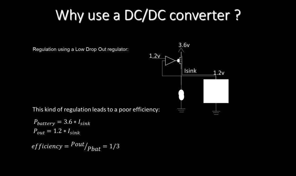
3 Why use a DC/DC converter? The SMPS converts the battery voltage to a lower voltage with high efficiency. That is, little power is lost in the converter itself. An SMPS output voltage of only 100mV above the LDO output voltage is sufficient for the LDO to perform normally. Thus, the LDO efficiency is in turn greatly improved. The role of the LDO is to filter the output voltage ripple produced by the SMPS. VbatPow 3.6V SMPS SMPS OUT LDO LDO OUT RF 1.2V GndPow Marc Sabut - STMicroelectronics 3
4 Switched Mode Power Supply (DC/DC buck converter) 1-Why use a DC/DC converter? 2-Architecture Marc Sabut - STMicroelectronics 4
5 Architecture Buck or down converter: output voltage is lower than the battery voltage. The following basic blocks combine to form a complete DC/DC converter: - Ramp generator - Error amplifier - Pulse Width Modulator - Control logic - Output filter Vmod All elements can be integrated except the output filter which is made up of an external inductor (some microh) and capacitors (some microf). A parameter to keep in mind for integration purpose is the thickness of these components which must be compatible with the package. Marc Sabut - STMicroelectronics 5
6 Architecture The error voltage is compared to the ramp voltage to produce a PWM signal which in turns set on or off the output power transistors. When the output voltage becomes lower than the reference voltage, the error signal increases so does the duty cycle of the PWM signal. Therefore, the power Pmos transistor is acting more frequently than the Nmos leading to a higher output current. Marc Sabut - STMicroelectronics 6
7 Architecture Vbat Pmos ON Pmos OFF The modulator output is a rectangular wave. This rectangle is averaged by the output filter and applied to the load. Vmod Vbat Ton T Toff t The duty cycle is defined as : D = T on T on + T off Marc Sabut - STMicroelectronics 7
8 Architecture The output DC voltage is therefore the average of the rectangular pulse waveform, or: V out = 1 T න 0 T V mod t dt = 1 t on T න Vbat dt = t on 0 T V bat V out = DV bat Where D is the duty cycle of the output and is defined as the time the output is connected to Vbat divided by the period of the witching frequency. Notice that the frequency of the ramp signal determines the frequency of the modulator output, which is the switching frequency of the converter. Marc Sabut - STMicroelectronics 8
9 Switched Mode Power Supply (DC/DC buck converter) 1-Why use a DC/DC converter? 2-Architecture 3-Conduction modes Continuous Conduction Mode Discontinuous Conduction Mode Marc Sabut - STMicroelectronics 9
10 Continuous conduction mode High current Iout Iself Iself > 0 t Iout Iself = 0 t Low current Iout Iself < 0 t Marc Sabut - STMicroelectronics 10
11 Vmod Continuous conduction mode Vbat T DTs (1-D)Ts Iself Iout (Vbat-Vout)/L (-Vout)/L I L I=0 Icapa Vout Imax Imin V DTs/2 (1-D)Ts/2 V OUT Marc Sabut - STMicroelectronics 11
12 Continuous conduction mode Current ripple: I L = V bat V out L DTs = V bat 1 D D L. F s Voltage ripple: V out = 1 C න 0 V out = (1 D)V bat LC DTs/2 (1 D)V bat L ( DTs 2 )2 2 1 V out = V bat 2 D(1 D) 8LCF S 1 D Ts/2 DV bat t dt + න t dt 0 L + DV bat LC (1 D) 2 Ts Marc Sabut - STMicroelectronics 12
13 Discontinuous conduction mode Iself High current Iout t Low current Iout t Marc Sabut - STMicroelectronics 13
14 Vmod Discontinuous conduction mode Vbat T DTs (1-D)Ts Iself Iout (Vbat-Vout)/L (-Vout)/L I L Iout=0 Icapa Imax I=0 Imin Marc Sabut - STMicroelectronics 14
15 Switched Mode Power Supply (DC/DC buck converter) 1-Why use a DC/DC converter? 2-Architecture 3-Conduction modes Continuous Conduction Mode Discontinuous Conduction Mode 4-Stability Voltage Mode Current Mode Modulator transfer function Filter transfer function Compensator transfer function Overall transfer function Marc Sabut - STMicroelectronics 15
16 Voltage mode regulation Vref Gain Ramp generator Compensation Network H2(p) Vramp Verror PWM Vmod LC filter H1(p) Vout This scheme comprises an error amplifier, a PWM modulator and an LC filter. It also includes a compensation network around the error amplifier to make the loop stable. This compensation network contains at least one pole and two zeros (to cope with the second order pole of the LC filter), the ultimate goal being to obtain a closed loop transfer function equivalent to a first order system. Marc Sabut - STMicroelectronics 16
17 Current mode regulation Vref Gain Ramp generator Compensation Network H2(p) Vramp PWM Vmod Iself LC filter H1(p) Vout In this kind of regulation, the inductor current is just subtracted to the output of the compensation network. This second internal loop helps to stabilize the system by forcing the loop to behave like a first order system in high frequency Marc Sabut - STMicroelectronics 17
18 Modulator transfer function Of the three blocks that make up the buck converter, the modulator is the only one with no frequency dependence. The modulator is basically a voltage-controlled rectangle wave generator. Vramp Verror Vmod Vbat Ton T Toff Thus, the duty cycle can be expressed as: D = T on T on + T off = V error V ramp Marc Sabut - STMicroelectronics 18
19 Modulator transfer function The modulator transfer function is the change in the average value of Vmod divided by a change in the error voltage: A mod = d V mod dv error = dv out dv error = d DV dv bat = d error dv error A mod = V bat V ramp V error V ramp V bat This is the gain of the modulator. In reality, this block has also time delays which cause phase shift. However, this phase shift usually is not a problem for the calculation of loop gain and phase and can be neglected in a first step. It will be addressed later in the design phase through transient simulation. (or by use of more advanced SPECTRE RF simulation). Marc Sabut - STMicroelectronics 19
20 Filter transfer function The modulator provides a pulse train, bounded by the battery voltage, whose duty cycle is determined by an applied control voltage. The output filter performs the averaging function that converts this pulse train into the output voltage of the converter. The cut-off frequency of the filter must therefore be an order of magnitude lower than the switching frequency. Because the goal of a dc/dc converter is to have high efficiency, the output filter consists of reactive components which do not dissipate power. This filter operates as a low pass filter in the frequency domain and is as simple as a second-order LC filter terminated by the load resistance. Therefore, the load resistance is a critical component of the filter and must be known in order to predict the filter s performance, the loop response and the stability of the converter. Marc Sabut - STMicroelectronics 20
21 Filter transfer function Ideal LC filter Marc Sabut - STMicroelectronics 21
22 Filter transfer function LC filter with parasitic Marc Sabut - STMicroelectronics 22
23 Filter transfer function At the cutoff frequency 1 the phase shift of -180dg is very sharp in an ideal filter and is somewhat LC smoothed in a real filter. These series resistances (usually referred to as ESR) in both the inductor and the output capacitor help to stabilize the loop. The gain slope is 40 db per decade of frequency increase above the LC cutoff frequency. From these considerations, we guess that two zeros have to be inserted in the loop to compensate for this brutal phase shift. The filter transfer function is then at first order: A filter = H 2 p = 1 1+ L R p+lcp2 Marc Sabut - STMicroelectronics 23
24 Compensator transfer function This chapter describes the design of the compensator for the voltage mode buck converter. The error amplifier has to amplify the difference between the reference voltage and the output voltage with sufficient accuracy (i.e. low static error). Its compensation network must also compensate for the 180dg phase shift of the LC filter in order to make the system stable (i.e. behaves like a derivator around the filter resonance frequency). Additionally, it must ensure sufficient bandwidth for the overall loop. Marc Sabut - STMicroelectronics 24
25 Compensator transfer function Vout Verror R 0 Compensator schematic Ro is inserted to set the DC level on node Vout: V out = 1 + R 1 R 0 V ref The compensator DC gain is then: Gain DC = R0 R0+R1. Gain opa Marc Sabut - STMicroelectronics 25
26 Compensator transfer function Vout Verror R 0 The compensator transfer function is then: Assuming an ideal opamp: A compensator = H 1 p = Compensator schematic A compensator = H 1 p = V error V out 1 R1 C1 + C2 p. 1 + R2 C2p (1 + R1 + R3 C3p) C1 C2 1 + R2 C1 + C2 p (1 + R3 C3p) Marc Sabut - STMicroelectronics 26
27 Compensator transfer function Gain opa =64dB R0/(R0+R1)=-11.5dB Gain DC =52.5dB Zero1 Zero2 Pole1 Pole2 Zero1: 1/R2.C2 Zero2: 1/R1.C3 (R3<<R1) Fu Fu : 1/R1.C2 (C1<<C2) Pole1: 1/R3.C3 Pole2: 1/R2.C1 (C1<<C2) Marc Sabut - STMicroelectronics 27


28 Compensator transfer function f<z1 : integrator p1 < f < p2: gain R3 z1 < f < z2 : c c gain p2 < f : c integrator z2 < f < p1: derivator Marc Sabut - STMicroelectronics 28
29 Overall transfer function Verror Vmod Vout Rload A mod = V bat V ramp H 2 p = 1 H 1 p 1 = R1 C1 + C2 p. 1 + R2 C2p (1 + R1 + R3 C3p) C1 C2 1 + R2 C1 + C2 p (1 + R3 C3p) 1 + L R p + LCp2 Marc Sabut - STMicroelectronics 29
30 Overall transfer function A classical strategy for placing the poles and zeros is demonstrated here. Besides deciding where to place the poles and zeros, the compensator gain also determines the crossover frequency of the loop. First, the loop crossover frequency has to be chosen and is based on the switching frequency and the desired loop transient response. Although the selection of the filter components have not been discussed, they are mainly chosen based on dynamic issues in the circuit design. Remember that the current ripple (respect. the voltage ripple) is inversely proportional to the L value (respect. to the LC product). Usually, the output inductor and capacitor are decided before the compensator design is started. The ESR(Electrical Serial Resistor) of these components have to be taken into account due to their impact on the efficiency and the stability of the loop. The roll-off behavior C=f(V) and the inductor saturation current L=f(IL) have also to be considered. (i.e. the inductance must be compatible with the maximum current involved). Marc Sabut - STMicroelectronics 30
31 Overall transfer function Step 1: Calculate the resistor R0 V ref Iref Given a current consumption Iref through R0: R 0 = Step 2: Calculate the Resistor Divider Values R 1 = R 0 V out Vref 1 Step 3: Calculate the filter s resonant frequency f LC = 1 2π LC Step 4: Place a first zero slightly below the filter s resonant frequency 1 C 3 = 2π. 0,9. f LC R 1 Step 5: Place a pole at the crossover frequency 1 R 3 = 2π. f crossover C 3 Marc Sabut - STMicroelectronics 31
32 Overall transfer function Step 6: Calculate the required gain of the compensator at the desired crossover frequency 1 H 1 (f crossover ) = A mod. H 2 (f crossover ) Step 7: Set the gain of the compensator R 2 = R 1 R 3. H 1 (f crossover ) (Note that at this frequency, the system behaves like an amplifier with a gain of R2/R3) Step 8: Place a second zero just below the filter resonance 1 C 2 = 2π. 0,9. f LC R 2 Step 9: Place a second pole about a decade above the crossover frequency 1 C 1 = 2π. 10. f crossover R 2 Marc Sabut - STMicroelectronics 32

33 Overall transfer function Marc Sabut - STMicroelectronics 33
34 Switched Mode Power Supply (DC/DC buck converter) 1-Why use a DC/DC converter? 2-Architecture 3-Conduction modes Continuous Conduction Mode Discontinuous Conduction Mode 4-Stability Voltage Mode Current Mode Modulator transfer function Filter transfer function Compensator transfer function Overall transfer function 5-Efficiency Marc Sabut - STMicroelectronics 34
35 Efficiency Since the battery provides an average current of Iout during the time D.Ts (and nothing during the remaining time (1-D).Ts ), its average current along a period Ts is: I BAT = I OUT. D. T s T S = I OUT. D The power provided by the battery can then be expressed as: P BAT = V BAT. I BAT = V BAT.D. I OUT The output power is given by: P OUT = V OUT. I OUT = D. V BAT. I OUT In case of an ideal DC/DC converter, the efficiency can then be expressed as: Efficiency = P OUT P BAT = 1 Of course, in a real world, some losses deteriorate the efficiency. Marc Sabut - STMicroelectronics 35
36 Efficiency Three kinds of losses degrade the efficiency of an SMPS. 1-Joules losses: They are due to the current which flows through the resistive path. output power Pmos : P pmos = Ron pmos. Iout 2.D output power Nmos : P nmos = Ron nmos. Iout 2.(1-D) ESR inductor: P esrl = R esrl. Iout 2 ESR capacitor: usually negligible Example: Vbat=3V Vout=1.5V Iload=20mA, Ronp=0.96Ω, Ronn=0.53Ω, ResrL=1.5Ω, ResrC=5mΩ output power Pmos : P pmos = 192 uw output power Nmos : P nmos = 106uW ESR inductor: P esrl = 600uW P joule = (Ron pmos. D + Ron nmos. 1 D + R esrl ). Iout 2 Marc Sabut - STMicroelectronics 36
 of the parasitic capacitors")


37 Efficiency 2-Switching losses: They originate from the charging(discharging) of the parasitic capacitors associated with each device. Vdd 2 Dynamic power in switched capacitor system: Vdd. I Vdd. C. Vdd Fs Pdyn Re q. Phase 1 Phase 2 P switch = 2. C gdp + C gdn + C db + C gs + C gb. V BAT 2. F s Marc Sabut - STMicroelectronics 37
38 Efficiency 2-Switching losses: Example: Cgs: NMOS +PMOS grid/source capacitor Cgb: NMOS +PMOS grid/bulk capacitor Cdb: NMOS +PMOS drain/bulk capacitor Cgd: NMOS +PMOS grid/drain capacitor P switch = 840uW : Cgs=2.51pF : Cgb=2.71pF : Cdb=2.8pF : Cgd=1.88pF 3-Quiescent losses: This comes from the bias current of each stage. P quies = I q. V BAT Example: Iq=200uA, Vbat=3V P quies =600uW 4-Efficiency: Ƞ = Example: Pout=60mW Ƞ = 96% P OUT P quies +P switch +P joule +P OUT Marc Sabut - STMicroelectronics 38
39 Efficiency Iout Marc Sabut - STMicroelectronics 39
40 Switched Mode Power Supply (DC/DC buck converter) 1-Why use a DC/DC converter? 2-Architecture 3-Conduction modes Continuous Conduction Mode Discontinuous Conduction Mode 4-Stability Voltage Mode Current Mode Modulator transfer function Filter transfer function Compensator transfer function Overall transfer function 5-Efficiency 6-Characteristics Marc Sabut - STMicroelectronics 40
41 Characteristics The various operating requirements are namely: - Battery voltage (Vbat) - Output voltage (Vout) - Output current range (Iout some ma) - Maximum output voltage ripple (Vripple some mv) - Clocking frequency (Fck some MHz) Notice that in RF design, the clock frequency must be chosen carefully depending on some spectrum specifications. Some additional requirements: - Load regulation : precision of output voltage while output current is changing - Load transient : response to an output current step - Line regulation : precision of output voltage while battery voltage is changing - Line transient : response to a battery voltage step - Efficiency (quiescent current) - Startup time Marc Sabut - STMicroelectronics 41
42 Characteristics Load transient : response to an output current step Vbat DC/DC converter Vout VOUT Some tens of mv Marc Sabut - STMicroelectronics 42
43 Characteristics Load regulation : precision of output voltage while output current is changing Vbat DC/DC converter Vout Iout Marc Sabut - STMicroelectronics 43
44 Characteristics Line transient : response to a battery voltage step Vbat DC/DC converter Vout VOUT Some tens of mv Marc Sabut - STMicroelectronics 44

45 Characteristics Line regulation : precision of output voltage while battery voltage is changing Vbat DC/DC converter Vout Vbat Marc Sabut - STMicroelectronics 45
46 Patent 1 et 2 Marc Sabut - STMicroelectronics 46

47 To add Boucle locale _ boucle globale _ Article de geelen Marc Sabut - STMicroelectronics 47
Monolithic CMOS Power Supply for OLED Display Driver / Controller IC
 Monolithic CMOS Power Supply for OLED Display Driver / Controller IC Cheung Fai Lee SOLOMON Systech Limited Abstract This paper presents design considerations of a power supply IC to meet requirements
Feedback: Part A - Basics
 Feedback: Part A - Basics Slides taken from: A.R. Hambley, Electronics, Prentice Hall, 2/e, 2000 1 Overview The Concept of Feedback Effects of feedback on Gain Effects of feedback on non linear distortion
RGB Encoder For the availability of this product, please contact the sales office. VIDEO OUT Y/C MIX DELAY CLAMP
 MATRIX Description The CXA1645P/M is an encoder IC that converts analog RGB signals to a composite video signal. This IC has various pulse generators necessary for encoding. Composite video outputs and
CXA1645P/M. RGB Encoder
 MATRIX CXA1645P/M RGB Encoder Description The CXA1645P/M is an encoder IC that converts analog RGB signals to a composite video signal. This IC has various pulse generators necessary for encoding. Composite
DIFFERENTIAL CONDITIONAL CAPTURING FLIP-FLOP TECHNIQUE USED FOR LOW POWER CONSUMPTION IN CLOCKING SCHEME
 DIFFERENTIAL CONDITIONAL CAPTURING FLIP-FLOP TECHNIQUE USED FOR LOW POWER CONSUMPTION IN CLOCKING SCHEME Mr.N.Vetriselvan, Assistant Professor, Dhirajlal Gandhi College of Technology Mr.P.N.Palanisamy,
VLSI Design: 3) Explain the various MOSFET Capacitances & their significance. 4) Draw a CMOS Inverter. Explain its transfer characteristics
 Explain the various MOSFET Capacitances & their significance. 4) Draw a CMOS Inverter. Explain its transfer characteristics") 1) Explain why & how a MOSFET works VLSI Design: 2) Draw Vds-Ids curve for a MOSFET. Now, show how this curve changes (a) with increasing Vgs (b) with increasing transistor width (c) considering Channel
1) Explain why & how a MOSFET works VLSI Design: 2) Draw Vds-Ids curve for a MOSFET. Now, show how this curve changes (a) with increasing Vgs (b) with increasing transistor width (c) considering Channel
PESIT Bangalore South Campus
 SOLUTIONS TO INTERNAL ASSESSMENT TEST 3 Date : 8/11/2016 Max Marks: 40 Subject & Code : Analog and Digital Electronics (15CS32) Section: III A and B Name of faculty: Deepti.C Time : 11:30 am-1:00 pm Note:
Lecture 3, Opamps. Operational amplifiers, high-gain, high-speed
 Lecture 3, Opamps Operational amplifiers, high-gain, high-speed What did we do last time? Multi-stage amplifiers Increases gain Increases number of poles Frequency domain Stability Phase margin 86 of 252
RF V W-CDMA BAND 2 LINEAR PA MODULE
 3 V W-CDMA BAND 2 LINEAR PA MODULE Package Style: Module, 10-Pin, 3 mm x 3 mm x 1.0 mm Features HSDPA and HSPA+ Compliant Low Voltage Positive Bias Supply (3.0 V to 4.35 V) +28.5 dbm Linear Output Power
Overview of All Pixel Circuits for Active Matrix Organic Light Emitting Diode (AMOLED)
") Chapter 2 Overview of All Pixel Circuits for Active Matrix Organic Light Emitting Diode (AMOLED) ---------------------------------------------------------------------------------------------------------------
Chapter 2 Overview of All Pixel Circuits for Active Matrix Organic Light Emitting Diode (AMOLED) ---------------------------------------------------------------------------------------------------------------
GS1881, GS4881, GS4981 Monolithic Video Sync Separators
 GS11, GS1, GS91 Monolithic Video Sync Separators DATA SHEET FEATURES noise tolerant odd/even flag, back porch and horizontal sync pulse fast recovery from impulse noise excellent temperature stability.5
EL302 DIGITAL INTEGRATED CIRCUITS LAB #3 CMOS EDGE TRIGGERED D FLIP-FLOP. Due İLKER KALYONCU, 10043
 EL302 DIGITAL INTEGRATED CIRCUITS LAB #3 CMOS EDGE TRIGGERED D FLIP-FLOP Due 16.05. İLKER KALYONCU, 10043 1. INTRODUCTION: In this project we are going to design a CMOS positive edge triggered master-slave
Timing Error Detection: An Adaptive Scheme To Combat Variability EE241 Final Report Nathan Narevsky and Richard Ott {nnarevsky,
 Timing Error Detection: An Adaptive Scheme To Combat Variability EE241 Final Report Nathan Narevsky and Richard Ott {nnarevsky, tomott}@berkeley.edu Abstract With the reduction of feature sizes, more sources
Efficient 500 MHz Digital Phase Locked Loop Implementation sin 180nm CMOS Technology
 Efficient 500 MHz Digital Phase Locked Loop Implementation sin 180nm CMOS Technology Akash Singh Rawat 1, Kirti Gupta 2 Electronics and Communication Department, Bharati Vidyapeeth s College of Engineering,
ECEN620: Network Theory Broadband Circuit Design Fall 2014
 ECEN620: Network Theory Broadband Circuit Design Fall 2014 Lecture 12: Divider Circuits Sam Palermo Analog & Mixed-Signal Center Texas A&M University Announcements & Agenda Divider Basics Dynamic CMOS
FMS3810/3815 Triple Video D/A Converters 3 x 8 bit, 150 Ms/s
 Triple Video D/A Converters 3 x 8 bit, 150 Ms/s Features 8-bit resolution 150 megapixels per second 0.2% linearity error Sync and blank controls 1.0V p-p video into 37.5Ω or 75Ω load Internal bandgap voltage
V6118 EM MICROELECTRONIC - MARIN SA. 2, 4 and 8 Mutiplex LCD Driver
 EM MICROELECTRONIC - MARIN SA 2, 4 and 8 Mutiplex LCD Driver Description The is a universal low multiplex LCD driver. The version 2 drives two ways multiplex (two blackplanes) LCD, the version 4, four
CHAPTER 3 SEPARATION OF CONDUCTED EMI
 54 CHAPTER 3 SEPARATION OF CONDUCTED EMI The basic principle of noise separator is described in this chapter. The construction of the hardware and its actual performance are reported. This chapter proposes
Communication and Computer Engineering ( CCE ) Prepared by
 Prepared by") Communication and Computer Engineering ( CCE ) Graduation Project Report Spring 2013 Digital TV Tuner Front End Design Part A : LNA and Mixer Prepared by 1. Ahmed Hesham Mohamed (1082011) 2. Mohamed Khaled
Communication and Computer Engineering ( CCE ) Graduation Project Report Spring 2013 Digital TV Tuner Front End Design Part A : LNA and Mixer Prepared by 1. Ahmed Hesham Mohamed (1082011) 2. Mohamed Khaled
Hello and welcome to this training module for the STM32L4 Liquid Crystal Display (LCD) controller. This controller can be used in a wide range of
 controller. This controller can be used in a wide range of") Hello and welcome to this training module for the STM32L4 Liquid Crystal Display (LCD) controller. This controller can be used in a wide range of applications such as home appliances, medical, automotive,
Hello and welcome to this training module for the STM32L4 Liquid Crystal Display (LCD) controller. This controller can be used in a wide range of applications such as home appliances, medical, automotive,
MAHARASHTRA STATE BOARD OF TECHNICAL EDUCATION (Autonomous)
") Subject Code: 17320 Model Answer Page 1 of 32 Important Instructions to examiners: 1) The answers should be examined by key words and not as word-to-word as given in the Model answer scheme. 2) The model
Subject Code: 17320 Model Answer Page 1 of 32 Important Instructions to examiners: 1) The answers should be examined by key words and not as word-to-word as given in the Model answer scheme. 2) The model
WINTER 15 EXAMINATION Model Answer
 Important Instructions to examiners: 1) The answers should be examined by key words and not as word-to-word as given in the model answer scheme. 2) The model answer and the answer written by candidate
A 5-Gb/s Half-rate Clock Recovery Circuit in 0.25-μm CMOS Technology
 A 5-Gb/s Half-rate Clock Recovery Circuit in 0.25-μm CMOS Technology Pyung-Su Han Dept. of Electrical and Electronic Engineering Yonsei University Seoul, Korea ps@tera.yonsei.ac.kr Woo-Young Choi Dept.
DEPARTMENT OF ELECTRONICS AND COMMUNICATION ENGINEERING SUBJECT CODE: CS1202 ELECTRONIC CIRCUITS AND DIGITAL SYSTEMS (FOR THIRD SEMESTER IT & CSE)
") DEPARTMENT OF ELECTRONICS AND COMMUNICATION ENGINEERING SUBJECT CODE: CS1202 ELECTRONIC CIRCUITS AND DIGITAL SYSTEMS (FOR THIRD SEMESTER IT & CSE) TWO MARK QUESTIONS &ANSWERS CS 1202: ELECTRONIC CIRCUITS
DEPARTMENT OF ELECTRONICS AND COMMUNICATION ENGINEERING SUBJECT CODE: CS1202 ELECTRONIC CIRCUITS AND DIGITAL SYSTEMS (FOR THIRD SEMESTER IT & CSE) TWO MARK QUESTIONS &ANSWERS CS 1202: ELECTRONIC CIRCUITS
American Power Design, Inc.
 FEATURES 4 Customer Selects Output Voltage 4 Outputs to 8000 Vdc 4 Proportional Output Voltage 4 Six-Sided Shielded Case 4 60 khz Switching Frequency 4 5000 Vdc Output Isolation 4 Continuous Short Circuit
QUICK START GUIDE FOR DEMONSTRATION CIRCUIT /12/14 BIT 10 TO 105 MSPS ADC
 LTC2280, LTC2282, LTC2284, LTC2286, LTC2287, LTC2288 LTC2289, LTC2290, LTC2291, LTC2292, LTC2293, LTC2294, LTC2295, LTC2296, LTC2297, LTC2298 or LTC2299 DESCRIPTION Demonstration circuit 851 supports a
MASSACHUSETTS INSTITUTE OF TECHNOLOGY Department of Electrical Engineering and Computer Science
 MASSACHUSETTS INSTITUTE OF TECHNOLOGY epartment of Electrical Engineering and Computer Science 6.374: Analysis and esign of igital Integrated Circuits Problem Set # 5 Fall 2003 Issued: 10/28/03 ue: 11/12/03
PEP-I1 RF Feedback System Simulation
 SLAC-PUB-10378 PEP-I1 RF Feedback System Simulation Richard Tighe SLAC A model containing the fundamental impedance of the PEP- = I1 cavity along with the longitudinal beam dynamics and feedback system
The high-end network analyzers from Rohde & Schwarz now include an option for pulse profile measurements plus, the new R&S ZVA 40 covers the
 GENERAL PURPOSE 44 448 The high-end network analyzers from Rohde & Schwarz now include an option for pulse profile measurements plus, the new R&S ZVA 4 covers the frequency range up to 4 GHz. News from
Analog, Mixed-Signal, and Radio-Frequency (RF) Electronic Design Laboratory. Electrical and Computer Engineering Department UNC Charlotte
 Electronic Design Laboratory. Electrical and Computer Engineering Department UNC Charlotte") Analog, Mixed-Signal, and Radio-Frequency (RF) Electronic Design Laboratory Electrical and Computer Engineering Department UNC Charlotte Teaching and Research Faculty (Please see faculty web pages for
Analog, Mixed-Signal, and Radio-Frequency (RF) Electronic Design Laboratory Electrical and Computer Engineering Department UNC Charlotte Teaching and Research Faculty (Please see faculty web pages for
NJU7241 Series. High-Precision LDO 60mA C-MOS Voltage Regulator with Standby TERMINAL DESCRIPTION PACKAGE OUTLINE
 High-Precision LDO 60mA C-MOS oltage Regulator with Standby GENERAL DESCRIPTION The NJU7241 series are high precision ±2%, 60mA output, C-MOS voltage regulators with standby function, which contains internal
25.5 A Zero-Crossing Based 8b, 200MS/s Pipelined ADC
 25.5 A Zero-Crossing Based 8b, 200MS/s Pipelined ADC Lane Brooks and Hae-Seung Lee Massachusetts Institute of Technology 1 Outline Motivation Review of Op-amp & Comparator-Based Circuits Introduction of
Simulation of DFIG and FSIG wind farms in. MATLAB SimPowerSystems. Industrial Electrical Engineering and Automation.
 CODEN:LUTEDX/(TEIE-7235)/1-007/(2009) Industrial Electrical Engineering and Automation Simulation of DFIG and FSIG wind farms in MATLAB SimPowerSystems Francesco Sulla Division of Industrial Electrical
Specifications. Reference Documentation. Performance Conditions
 The material in this section is organized into two main groupings: the specification tables and the supporting figures. The specification tables include: 1. PAL general and test signal specifications 2.
A MISSILE INSTRUMENTATION ENCODER
 A MISSILE INSTRUMENTATION ENCODER Item Type text; Proceedings Authors CONN, RAYMOND; BREEDLOVE, PHILLIP Publisher International Foundation for Telemetering Journal International Telemetering Conference
Datasheet SHF A
 SHF Communication Technologies AG Wilhelm-von-Siemens-Str. 23D 12277 Berlin Germany Phone +49 30 772051-0 Fax ++49 30 7531078 E-Mail: sales@shf.de Web: http://www.shf.de Datasheet SHF 19120 A 2.85 GSa/s
King Fahd University of Petroleum and Minerals Electrical Engineering Department 1. Homework 5 - SOLUTION KEY
 Electrical Engineering Department 1 Homework 5 - SOLUTION KEY EE-306 Electromechanical Devices - Semester 162 Electrical Engineering Department 2 Problem 1 Consider a Europeon city, it is necessary to
Logic Gates, Timers, Flip-Flops & Counters. Subhasish Chandra Assistant Professor Department of Physics Institute of Forensic Science, Nagpur
 Logic Gates, Timers, Flip-Flops & Counters Subhasish Chandra Assistant Professor Department of Physics Institute of Forensic Science, Nagpur Logic Gates Transistor NOT Gate Let I C be the collector current.
Very low-noise, high-efficiency DC-DC conversion circuit
 DN0013 Design note Very low-noise, high-efficiency DC-DC conversion circuit Designs from our labs describe tested circuit designs from ST labs which provide optimized solutions for specific applications.
Report on 4-bit Counter design Report- 1, 2. Report on D- Flipflop. Course project for ECE533
 Report on 4-bit Counter design Report- 1, 2. Report on D- Flipflop Course project for ECE533 I. Objective: REPORT-I The objective of this project is to design a 4-bit counter and implement it into a chip
A FOUR GAIN READOUT INTEGRATED CIRCUIT : FRIC 96_1
 A FOUR GAIN READOUT INTEGRATED CIRCUIT : FRIC 96_1 J. M. Bussat 1, G. Bohner 1, O. Rossetto 2, D. Dzahini 2, J. Lecoq 1, J. Pouxe 2, J. Colas 1, (1) L. A. P. P. Annecy-le-vieux, France (2) I. S. N. Grenoble,
Energy Recovery Clocking Scheme and Flip-Flops for Ultra Low-Energy Applications
 Energy Recovery Clocking Scheme and Flip-Flops for Ultra Low-Energy Applications Matthew Cooke, Hamid Mahmoodi-Meimand, Kaushik Roy School of Electrical and Computer Engineering, Purdue University, West
Understanding. Here s an examination of high-frequency pathological signal transmission issues in today s high-bandwidth equipment.
 Understanding Feature blocking capacitor effects Here s an examination of high-frequency pathological signal transmission issues in today s high-bandwidth equipment. By Renaud Lavoie W hy should we do
Analog Circuits Prof. Nagendra Krishnapura Department of Electrical Engineering Indian Institute of Technology, Madras. Module - 04 Lecture 12
 Analog Circuits Prof. Nagendra Krishnapura Department of Electrical Engineering Indian Institute of Technology, Madras Module - 04 Lecture 12 So, far we have discussed common source amplifier using an
Maintenance/ Discontinued
 A/D, D/C Converters for Image Signal Processing MN6570F, MN6570TF, and MN6570EF Low Power 8-Bit, 3-Channel CMOS D/A Converters for Image Processing Overview The MN6570F, MN6570TF, and MN6570EF are highspeed
DESIGN OF DOUBLE PULSE TRIGGERED FLIP-FLOP BASED ON SIGNAL FEED THROUGH SCHEME
 Scientific Journal Impact Factor (SJIF): 1.711 e-issn: 2349-9745 p-issn: 2393-8161 International Journal of Modern Trends in Engineering and Research www.ijmter.com DESIGN OF DOUBLE PULSE TRIGGERED FLIP-FLOP
Dual Slope ADC Design from Power, Speed and Area Perspectives
 Dual Slope ADC Design from Power, Speed and Area Perspectives Isaac Macwan, Xingguo Xiong, Lawrence Hmurcik Department of Electrical & Computer Engineering, University of Bridgeport, Bridgeport, CT 06604
Product Specification PE613010
 Product Description The is an SPST tuning control switch based on Peregrine s UltraCMOS technology. This highly versatile switch supports a wide variety of tuning circuit topologies with emphasis on impedance
Advanced Test Equipment Rentals ATEC (2832)
") Established 1981 Advanced Test Equipment Rentals www.atecorp.com 800-404-ATEC (2832) This product is no longer carried in our catalog. AFG 2020 Characteristics Features Ordering Information Characteristics
Established 1981 Advanced Test Equipment Rentals www.atecorp.com 800-404-ATEC (2832) This product is no longer carried in our catalog. AFG 2020 Characteristics Features Ordering Information Characteristics
QUICK START GUIDE FOR DEMONSTRATION CIRCUIT /12/14 BIT 10 TO 65 MSPS DUAL ADC
 LTC2286, LTC2287, LTC2288, LTC2290, LTC2291, LTC2292, LTC2293, LTC2294, LTC2295, LTC2296, LTC2297, LTC2298 or LTC2299 DESCRIPTION Demonstration circuit 816 supports a family of s. Each assembly features
Parametric Optimization of Clocked Redundant Flip-Flop Using Transmission Gate
 Parametric Optimization of Clocked Redundant Flip-Flop Using Transmission Gate Sapna Sadhwani Student, Department of ECE Lakshmi Narain College of Technology Bhopal, India srsadhwani@gmail.comm Abstract
Asynchronous Design for Analogue Electronics. Alex Yakovlev
 Asynchronous Design for Analogue Electronics Alex Yakovlev Motivation: A4A scope conventional RTL synthesis IP core (big digital) IP core (big digital) ADC sensor sensor DAC analogue components power converter
Lecture 17 Microwave Tubes: Part I
 Basic Building Blocks of Microwave Engineering Prof. Amitabha Bhattacharya Department of Electronics and Communication Engineering Indian Institute of Technology, Kharagpur Lecture 17 Microwave Tubes:
DATASHEET EL4583A. Features. Applications. Pinout. Ordering Information. Sync Separator, 50% Slice, S-H, Filter, HOUT. FN7503 Rev 2.
 DATASHEET Sync Separator, 50% Slice, S-H, Filter, HOUT FN7503 Rev 2.00 The extracts timing from video sync in NTSC, PAL, and SECAM systems, and non-standard formats, or from computer graphics operating
HIGH VOLTAGE SWITCH PERFORMANCE OF THE EIMAC X-2159 TETRODE ABSTRACT
 HIGH VOLTAGE SWITCH PERFORMANCE OF THE EIMAC X-2159 TETRODE by Bobby R. Gray High Power Component & Effects Section Techniques Branch Surveillance Division Rome Air Development Center Griffiss Air Force
Sensor Development for the imote2 Smart Sensor Platform
 Sensor Development for the imote2 Smart Sensor Platform March 7, 2008 2008 Introduction Aging infrastructure requires cost effective and timely inspection and maintenance practices The condition of a structure
LOW POWER LEVEL CONVERTING FLIP-FLOP DESIGN BY USING CONDITIONAL DISCHARGE TECHNIQUE
 LOW POWER LEVEL CONVERTING FLIP-FLOP DESIGN BY USING CONDITIONAL DISCHARGE TECHNIQUE Keerthana S Assistant Professor, Department of Electronics and Telecommunication Engineering Karpagam College of Engineering
Troubleshooting EMI in Embedded Designs White Paper
 Troubleshooting EMI in Embedded Designs White Paper Abstract Today, engineers need reliable information fast, and to ensure compliance with regulations for electromagnetic compatibility in the most economical
Interpolated DDS Technique in SDG2000X October 24, 2017 Preface
 Interpolated DDS Technique in SDG2000X October 24, 2017 Preface As can be seen in the data sheet for Siglent s SDG2000X arbitrary waveform generator series, the sampling rate specification (1.2 GSa/s)
psasic Timing Generator
 psasic Timing Generator Fukun Tang psasic Design Review July 1-2 2009 University of Chicago 1 Diagram of 40Gs/s Sampling Chip CLOCK (80MHz) IN(1:32) Timing Generator with 2 DLLs interleaved PD CP LF φ1
SatLabs Recommendation for a Common Inter-Facility Link for DVB-RCS terminals
 SatLabs Recommendation for a Common Inter-Facility Link for DVB-RCS terminals Version 1.6-06/01/2005 This document is the result of a cooperative effort undertaken by the SatLabs Group. Neither the SatLabs
Obsolete Product(s) - Obsolete Product(s)
 - Obsolete Product(s)") L4902A DUAL 5 REGULATOR WITH RESET AND DISABLE DOUBLE BATTERY OPERATING OUTPUT CURRENTS : I01 = 300 ma I02 = 300 ma FIXED PRECISION OUTPUT OLTAGE 5 ± 2 % RESET FUNCTION CONTROLLED BY INPUT OLTAGE AND OUTPUT
L4902A DUAL 5 REGULATOR WITH RESET AND DISABLE DOUBLE BATTERY OPERATING OUTPUT CURRENTS : I01 = 300 ma I02 = 300 ma FIXED PRECISION OUTPUT OLTAGE 5 ± 2 % RESET FUNCTION CONTROLLED BY INPUT OLTAGE AND OUTPUT
PMP15002 Test Results
 Test Report Aug 2016 PMP15002 Test Results Note that this reference design is not an orderable device from TI, but shows the performance of a UCC28704/UCC24636 in a constant voltage/ constant current controller
TMC3503 Triple Video D/A Converter 8 bit, 80 Msps, 5V
 Triple Video D/A Converter 8 bit, 80 Msps, 5V Features 8-bit resolution 80, 50, and 30 megapixels per second ±0.5 LSB linearity error Sync, blank, and white controls Independent sync current output 1.0V
LED driver architectures determine SSL Flicker,
 LED driver architectures determine SSL Flicker, By: MELUX CONTROL GEARS P.LTD. Replacing traditional incandescent and fluorescent lights with more efficient, and longerlasting LED-based solid-state lighting
Chapter 5 Flip-Flops and Related Devices
 Chapter 5 Flip-Flops and Related Devices Chapter 5 Objectives Selected areas covered in this chapter: Constructing/analyzing operation of latch flip-flops made from NAND or NOR gates. Differences of synchronous/asynchronous
SDA 3302 Family. GHz PLL with I 2 C Bus and Four Chip Addresses
 GHz PLL with I 2 C Bus and Four Chip Addresses Preliminary Data Features 1-chip system for MPU control (I 2 C bus) 4 programmable chip addresses Short pull-in time for quick channel switch-over and optimized
ML6428. S-Video Filter and 75Ω Line Drivers with Summed Composite Output. Features. General Description. Block Diagram Σ BUFFER.
 www.fairchildsemi.com ML S-Video Filter and Line Drivers with Summed Composite Output Features.MHz Y and C filters, with CV out for NTSC or PAL cable line driver for Y, C, CV, and TV modulator db stopband
FDTD_SPICE Analysis of EMI and SSO of LSI ICs Using a Full Chip Macro Model
 FDTD_SPICE Analysis of EMI and SSO of LSI ICs Using a Full Chip Macro Model Norio Matsui Applied Simulation Technology 2025 Gateway Place #318 San Jose, CA USA 95110 matsui@apsimtech.com Neven Orhanovic
P.Akila 1. P a g e 60
 Designing Clock System Using Power Optimization Techniques in Flipflop P.Akila 1 Assistant Professor-I 2 Department of Electronics and Communication Engineering PSR Rengasamy college of engineering for
ECE438 - Laboratory 4: Sampling and Reconstruction of Continuous-Time Signals
 Purdue University: ECE438 - Digital Signal Processing with Applications 1 ECE438 - Laboratory 4: Sampling and Reconstruction of Continuous-Time Signals October 6, 2010 1 Introduction It is often desired
Integrated Circuit for Musical Instrument Tuners
 Document History Release Date Purpose 8 March 2006 Initial prototype 27 April 2006 Add information on clip indication, MIDI enable, 20MHz operation, crystal oscillator and anti-alias filter. 8 May 2006
GHZ to 43.5 GHz envelope detector
 1.0 This specification documents the detail requirements for space qualified product manufacturing on Analog Devices, Inc. s QML certified line per MIL-PRF-38535 Level V except as modified herein. The
A Power Efficient Flip Flop by using 90nm Technology
 A Power Efficient Flip Flop by using 90nm Technology Mrs. Y. Lavanya Associate Professor, ECE Department, Ramachandra College of Engineering, Eluru, W.G (Dt.), A.P, India. Email: lavanya.rcee@gmail.com
Why Engineers Ignore Cable Loss
 Why Engineers Ignore Cable Loss By Brig Asay, Agilent Technologies Companies spend large amounts of money on test and measurement equipment. One of the largest purchases for high speed designers is a real
STEVAL-ISA001V1. 6W Dual Output Supply using VIPer12A. Features. Blue angel. Applications
 Features Switch mode General Purpose Power Supply Input: 85 to 264 VAC @ 50/60 Hz Output: 12V @ 0.5A Output Power (peak) 6W Burst Mode Operation in Standby for Blue Angel operation Current Mode Control
Obsolete Product(s) - Obsolete Product(s)
 - Obsolete Product(s)") L4937N DUAL MULTIFUNCTION OLTAGE REGULATOR STANDBY OUTPUT OLTAGE PRECISION 5 ± 2% OUTPUT 2 TRACKED TO THE STANDBY OUT- PUT OUTPUT 2 DISABLE FUNCTION FOR STANDBY MODE ERY LOW QUIESCENT CURRENT, LESS THAN
L4937N DUAL MULTIFUNCTION OLTAGE REGULATOR STANDBY OUTPUT OLTAGE PRECISION 5 ± 2% OUTPUT 2 TRACKED TO THE STANDBY OUT- PUT OUTPUT 2 DISABLE FUNCTION FOR STANDBY MODE ERY LOW QUIESCENT CURRENT, LESS THAN
ECB DIGITAL ELECTRONICS PROJECT BASED LEARNING PROJECT REPORT ON 7 SEGMENT DIGITAL STOP WATCH USING DECODER
 ECB2212 - DIGITAL ELECTRONICS PROJECT BASED LEARNING PROJECT REPORT ON 7 SEGMENT DIGITAL STOP WATCH USING DECODER SUBMITTED BY ASHRAF HUSSAIN (160051601105) S SAMIULLAH (160051601059) CONTENTS >AIM >INTRODUCTION
EL4583. Features. Sync Separator, 50% Slice, S-H, Filter, H OUT. Applications. Ordering Information. Pinout FN Data Sheet March 28, 2013
 Data Sheet FN7173.4 Sync Separator, 50% Slice, S-H, Filter, H OUT The EL4583 extracts timing from video sync in NTSC, PAL, and SECAM systems, and non standard formats, or from computer graphics operating
DATASHEET EL1883. Features. Applications. Ordering Information. Demo Board. Pinout. Sync Separator with Horizontal Output. FN7010 Rev 2.
 DATASHEET EL883 Sync Separator with Horizontal Output FN7 Rev 2. The EL883 video sync separator is manufactured using Elantec s high performance analog CMOS process. This device extracts sync timing information
Precise Digital Integration of Fast Analogue Signals using a 12-bit Oscilloscope
 EUROPEAN ORGANIZATION FOR NUCLEAR RESEARCH CERN BEAMS DEPARTMENT CERN-BE-2014-002 BI Precise Digital Integration of Fast Analogue Signals using a 12-bit Oscilloscope M. Gasior; M. Krupa CERN Geneva/CH
DIGITAL ELECTRONICS MCQs
 DIGITAL ELECTRONICS MCQs 1. A 8-bit serial in / parallel out shift register contains the value 8, clock signal(s) will be required to shift the value completely out of the register. A. 1 B. 2 C. 4 D. 8
CVOUT Vcc2 TRAP SWITCH Y/C MIX INTERNAL TRAP DELAY LPF LPF SIN-PULSE NPIN SCIN
 R G B SC NP BFOUT MATRIX GND2 ROUT GOUT BOUT CVOUT Vcc2 Y YOUT COUT RGB Encoder CXA20M Description The CXA20M is an encoder IC that converts analog RGB signals a composite video signal. This IC has various
Pre-emphasis Buffer modeling
 Pre-emphasis Buffer modeling Hazem Hegazy Fady Galal Roshdy Hegazy Speaker notes is present in this foils. 1 Agenda Introduction DC through Transient simulation Modeling Technique (1) (One Model, No driver
CHAPTER 6 ASYNCHRONOUS QUASI DELAY INSENSITIVE TEMPLATES (QDI) BASED VITERBI DECODER
 BASED VITERBI DECODER") 80 CHAPTER 6 ASYNCHRONOUS QUASI DELAY INSENSITIVE TEMPLATES (QDI) BASED VITERBI DECODER 6.1 INTRODUCTION Asynchronous designs are increasingly used to counter the disadvantages of synchronous designs.
80 CHAPTER 6 ASYNCHRONOUS QUASI DELAY INSENSITIVE TEMPLATES (QDI) BASED VITERBI DECODER 6.1 INTRODUCTION Asynchronous designs are increasingly used to counter the disadvantages of synchronous designs.
Matthew Reid Powell. A uthor... Department of Electrical Engineering and Computer Science March 12, 2004
 Integrated Feedback Circuit for Organic LED Display Driver by Matthew Reid Powell Submitted to the Department of Electrical Engineering and Computer Science in partial fulfillment of the requirements for
TEST REPORT T&M Research Products, Inc. Model W11K20-3.5s Ω by M. E. Gruchalla PE, December 6, 2008
 TEST REPORT T&M Research Products, Inc. Model W11K20-3.5s-0.0002433Ω by M. E. Gruchalla PE, December 6, 2008 1. INTRODUCTION A T&M Research Products, Inc. Model W11K20-3.5s-0.0002433Ω Current Viewing Resistor
COHERENCE ONE PREAMPLIFIER
 COHERENCE ONE PREAMPLIFIER OWNER S MANUAL TABLE OF CONTENTS Introduction Features Unpacking Instructions Installation Phono Cartridge Loading Basic Troubleshooting Technical Specifications Introduction
4-Channel Video Reconstruction Filter
 19-2948; Rev 1; 1/5 EVALUATION KIT AVAILABLE 4-Channel Video Reconstruction Filter General Description The 4-channel, buffered video reconstruction filter is ideal for anti-aliasing and DAC-smoothing video
BGA2022, RX mixer 880, 1950 and 2450 MHz
 Philips Semiconductors BGA2022, RX mixer 880, 1950 and 2450 MHz Application Note AN00059 APPLICATION NOTE BGA2022, RX mixer 880, 1950 and 2450 MHz AN00059 Author(s): Hans ten Cate Philips Semiconductors
Calibrate, Characterize and Emulate Systems Using RFXpress in AWG Series
 Calibrate, Characterize and Emulate Systems Using RFXpress in AWG Series Introduction System designers and device manufacturers so long have been using one set of instruments for creating digitally modulated
T sors, such that when the bias of a flip-flop circuit is
 EEE TRANSACTONS ON NSTRUMENTATON AND MEASUREMENT, VOL. 39, NO. 4, AUGUST 1990 653 Array of Sensors with A/D Conversion Based on Flip-Flops WEJAN LAN AND SETSE E. WOUTERS Abstruct-A silicon array of light
Low-Noise Downconverters through Mixer-LNA Integration
 Low-Noise Downconverters through Mixer-LNA Integration Carlos E. Saavedra Associate Professor Dept. of Electrical & Comp. Engineering Queen s University, Kingston, Ontario CANADA IEEE International Microwave
BASIC LINEAR DESIGN. Hank Zumbahlen Editor Analog Devices, Inc. All Rights Reserved
 BASIC LINEAR DESIGN Hank Zumbahlen Editor A 2007 Analog Devices, Inc. All Rights Reserved Preface: This work is based on the work of many other individuals who have been involved with applications and
Experiment 9 Analog/Digital Conversion
 Experiment 9 Analog/Digital Conversion Introduction Most digital signal processing systems are interfaced to the analog world through analogto-digital converters (A/D) and digital-to-analog converters
BTV Tuesday 21 November 2006
 Test Review Test from last Thursday. Biggest sellers of converters are HD to composite. All of these monitors in the studio are composite.. Identify the only portion of the vertical blanking interval waveform
CAT Channel Ultra High Efficiency LED Driver with 32 Dimming Levels
 4-Channel Ultra High Efficiency LED Driver with 32 Dimming Levels Description The CAT3648 is a high efficiency fractional charge pump that can drive up to four LEDs programmable by a one wire digital interface.
ST2225A. LED Display Driver. Version : A.025 Issue Date : 2001/11/26 File Name Total Pages : 12. : SP-ST2225A-A.025.doc
 Version : A.025 Issue Date : 2001/11/26 File Name Total Pages : 12 : SP--A.025.doc LED Display Driver 新竹市科學園區展業㆒路 9 號 7 樓之 1 9-7F-1, Prosperity Road I, Science Based Industrial Park, Hsin-Chu, Taiwan 300,
United States Patent (19) Mizomoto et al.
 Mizomoto et al.") United States Patent (19) Mizomoto et al. 54 75 73 21 22 DIGITAL-TO-ANALOG CONVERTER Inventors: Hiroyuki Mizomoto; Yoshiaki Kitamura, both of Tokyo, Japan Assignee: NEC Corporation, Japan Appl. No.: 18,756
United States Patent (19) Mizomoto et al. 54 75 73 21 22 DIGITAL-TO-ANALOG CONVERTER Inventors: Hiroyuki Mizomoto; Yoshiaki Kitamura, both of Tokyo, Japan Assignee: NEC Corporation, Japan Appl. No.: 18,756
Modify the UL40-S2 into a Super-Triode amplifier. Ir. Menno van der Veen
 Modify the UL40-S2 into a Super-Triode amplifier Ir. Menno van der Veen Introduction about modifications: The UL40-S2 is already some years on the market and meanwhile I have received several requests