Memory Based Computing for DSP. Pramod Meher Institute for Infocomm Research
|
|
|
- Thomasine Agatha Davis
- 5 years ago
- Views:
Transcription
1 Memory Based Computing for DSP Applications Pramod Meher Institute for Infocomm Research Singapore
2 outline trends in memory technology memory based computing: advantages and examples DA based computation for DSP applications lookup table design for constant multiplication li li i DA based vs LUT multiplier based implementations memory based evaluation of non linear functions conclusions 2
3 trends in memory technology Application specific memories [1 4] low power memories for mobile devices and consumer products high speed memories for multimedia applications wide temperature memories for automotive high reliability memoriesfor biomedicalinstruments instruments radiation hardened memory for space applications 3
4 trends in memory technology RAM logic integration several nonvolatile RAM types are emerging: ferroelectric RAM (FeRAM), magneto resistive RAM (MRAM), and varieties of phase change memory (PCM) [4 6] the upcoming/new memories provide faster access and consume less power [4 6] can be embedded directly into the structure of microprocessors or integrated in the functional elements of dedicated processors [7] 4
5 trends in memory technology memory placement [7 11] traditional concept of memory as a stand alone subsystem is getting changed itisembedded is withinthe the logiccomponents components processor has been moved to memory or memory has been moved to processor the relocations result in higher bandwidth, lower power consumption and less access delay 5
6 memory-based computing? a class of dedicated systems, where the computational functions are performed by lookuptables (LUTs), instead of actual calculations close to human like computing simple to design, and more regular compared with the multiply accumulate structures have potential for high throughput and reducedlatency implementation involves less dynamic power consumption due to minimization of switching activities 6
7 memory-based computations: examples inner product computation using the distributed arithmetic (DA) [12] direct implementation of constant multiplications [13] well suited for digital it filtering i and orthogonal transformations for digital signal processing implementation of fixed and adaptive FIR filters and transforms other applications: evaluation of trigonometric functions, sigmoid and other nonlinear function 7
8 DA to calculate inner-product : example X = [X 0 X 1 X 2 ] T and A = [A 0, A 1, A 2 ] T : 3-point vectors. A is constant X 0, X 1 and X 2 be 4-bit integers: X 0 = [ x 0 (3) x 0 (2) x 0 (1) x 0 (0)] X 1 = [ x 1 (3) x 1 (2) x 1 (1) x 1 (0)] X 2 = [ x 2 (3) x 2 (2) x 2 (1) x 2 (0)] inner-product of X and A : A.X =A 0 X 0 + A 1 X 1 + A 2 X 2 P 0 P 1 P 2 P 3 inner-product of : AX A.X = P 0 +2P 1 +4P 2 +8P 3 12/17/2010 Institute for Infocomm Research, Singapore 8
9 LUT for inner-product using DA [12] x 2 (i) x 1 (i) x 0 (i) partial sum A A A 1 +A A A 2 +A A 2 +A A 2 +A 1 +A 0 x 0 (3) x 1 (3) x 2 (3) x 0 (2) x 1 (2) x 2 (2) x 0 (1) x 1 (1) x 2 (1) x 0 (0) x 1 (0) x 2 (0) 3 TO 8 LINE DECODER LUT 0 A 0 A 1 A 1 +A 0 A 2 A 2 +A 0 A 2 +A 1 A 2 +A 1+A 0 inner-product A.X + shift right 2^N LUT words required for N-point inner-product. For N=32, it exceeds 10^9 words!! For L-bit inputs, computation time = L cycles : Cycle time, T=T MEM + T ADD + T FF 12/17/2010 Institute for Infocomm Research, Singapore 9
10 LUT compaction for DA [12] x 2 (i) x 1 (i) x 0 (i) conventional OBC LUT content (A 2 +A 1 +A 0 ) A 0 -(A 2 +A 1 -A 0 ) A 1 -(A 2 -A 1 +A 0 ) A 1 +A 0 -(A 2 -A 1 -A 0 ) A 2 (A 2 -A 1 -A 0 ) A 2 +A 0 (A 2 -A 1 +A 0 ) A 2 +A 1 ( A 2 +A 1 -A 0 ) A 2 +A 1 +A 0 (A 2 +A 1 +A 0 ) Desired partial sum of product = [OBC value + (A 2 +A 1 +A 0 )]/2 half the number of LUT words are saved if OBC is used 10
11 linear convolution/ FIR filtering [13] x[n] h[0] N-tap FIR filter equation: address LUT content y[n]=h[0] h[0].x[n]+ h[1].x[n-1] h[n-1].x[n-n+1] direct-form FIR filter for N=4. 4 X D h[1] x[n-1] 4 point inner product. Weights are constant X h[0] 0010 h[1] 0011 h[1]+h[0] 0100 h[2] 0101 h[2]+h[0] D x[n-2] x[n-3] 0110 h[2]+h[1] D 0111 h[2]+h[1]+h[0] h[2] 1000 h[3] h[3] X X 1001 h[3]+h[0] 1010 h[3]+h[1] 1011 h[3] +h[1]+h[0] 1100 h[3] +h[2] 1101 h[3] +h[2]+h[0] 1110 h[3] +h[2]+h[1] y[n] 1111 h[3] +h[2]+h[1]+h[0] 12/17/2010 Institute for Infocomm Research, Singapore 11
12 DA-based adaptive filtering [14] example: 4 tap FIR adaptive filter 4 point inner product. Weights are not constant. x[n] x[n-1] x[n-2] x[n-3] D D D h[0] h[1] h[2] h[3] X X X X weightupdate y[n] + d[n] e[n] 12


13 LUT for adaptive filter: example [14] address LUT values LUT values address bits of the same place values of the filter coefficients are used as addresses 13
14 DA-based inner-product of long vectors AX N 1 P1 2P1 MP1 n 0 A n X n n 0 A n X n np A n X n A n np ( M 1) X n for N=MP Inner Product Inner Product Inner Product Unit 1 Unit 2 Unit P inner-product A.X P LUTs of 2^(M) words and (P-1) adders required for N-point p inner-product. 12/17/2010 Institute for Infocomm Research, Singapore 14
15 large order FIR filter using DA [15] x[n] M INPUT SHIFT-REGISTER x[n-1] x[n-n+2] BIT-SERIAL WORD-PARALLEL CONVERTER M (b n ) 0,0 (b n ) 0,1 (b n ) 0,(P-1) (b n ) 1,0 (b n ) 1,1 (b n ) 1,(P-1) Xin M x[n-n+1] Xin Yin PE Xout Xout Xin ROM _ Read( Yin). OUTPUT CELL Xout (b n ) (L-1),0 (b n ) (L-1),1 (b n ) (L-1),(P-1) 0 PE PE PE (P-1) OUTPUT CELL OUTPUT (b n ) i,j :(j+1)th segment of bit-vector of ith bits of input Initialize : S 0; Count 0; End Initialization. For 0 Count L 1: S 2S Xin; Count Count 1. If Count L then Xout S; S 0; Count 0; Endif. 15
16 large order FIR filter: a 2-D design [15] BIT-PARA LLEL WORD-S SERIAL CONVE ERTER SERIAL-IN PARALLEL-OUT SHIFT-REGISTER (P-1) M M M 0 PE PE PE SERIAL-IN PARALLEL-OUT SHIFT-REGISTER (P-1) M M M 0 PE PE PE (L-2) SERIAL-IN PARALLEL-OUT SHIFT-REGISTER (P-1) M M M 0 SA SA Yin Xin SA Yout Yout Xin 2. Yin Yin Xin PE Xout INPUT 0 PE PE PE (L-1) SA Xout Xin ROM _ Read( Yin). OUTPUT 12/17/2010 Institute for Infocomm Research, Singapore 16
17 circular Convolution using DA [16] circular convolution of two N-point sequences {x(n)} and {h(n)} is : circular convolution for N=4: 4 17
18 cyclic convolution using DA: a 2-D design [16] (L)-th bit-stream of input sequence {x(n)} BIT-PARALL LEL WORD-SE ERIAL CONVER RTER CIRCULRLY RIGHT-SHIFT BUFFER (P-1) M M M 0 PE PE PE second bit-stream of input sequence {x(n)} CIRCULRLY RIGHT-SHIFT BUFFER (P-1) M M M 0 PE PE PE (L-2) first bit-stream of input sequence {x(n)} 0 SA SA INPUT SAMPLES CIRCULRLY RIGHT-SHIFT BUFFER (P-1) M M M 0 PE PE PE (L-1) SA OUTPUT 12/17/2010 Institute for Infocomm Research, Singapore 18
19 computation of sinusoidal transforms [17-20] N-point sinusoidal transforms like the DFT, DCT and DHT are given by where the transform kernel is defined as computation of N-point sinusoidal transforms involves multiplication of an N x N kernel matrix with N-point input vectors involves N number of inner-products of N-point input vector with the rows of kernel matrix the matrix-vector product requires N inner-product computation units by the DA approach for prime values of N, the N x N kernel matrix is transformed to an (N-1)- point cyclic convolution. 12/17/2010 Institute for Infocomm Research, Singapore 19
20 multiplication using look-up-table X multiplication of an L-bit number X with ih L constant A will require an LUT of 2 L LUT OF words 2^L Words multiplication time = memory latency AX LUT to multiply a 4-bit word X with a constant A address word, X product word address word, X product word A 0001 A A A A A A A A A A A A A A LUT size increases exponentially with input size. 12/17/2010 Institute for Infocomm Research, Singapore 20
21 optimization for constant multiplications odd multiple storage (OMS) scheme anti symmetric product coding (APC) scheme input coding (IC) scheme combined techniques 21
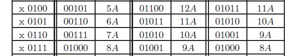
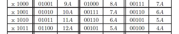
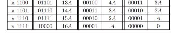
22 odd-multiple storage scheme [21] address word product word A A A A A A A address word product word A A A A A A A A address word product word 0001 A A A A A A A A Only odd multiple of the constant are to be stored in the LUT. Even multiples could be derived from the stored words. Only half the number of product words are to be saved. 12/17/2010 Institute for Infocomm Research, Singapore 22
23 odd-multiple storage scheme [21] memory unit of (2^L)/2 words of (W+L) bit width is used to store the odd multiples l of constant ta. a barrel shifter for producing a maximum of (L-1) leftshifts is used to derive all the even multiples of A. the L bit input word is mapped to (L-1)-bit address of the LUT by an encoder. the control bits for barrel shifter are derived by a control circuit to perform the necessary shifts of the LUT output. RESET signal is generated by the same control circuit to resetthelut the outputwhenthex=0 the X 0. if only magnitude part could be used as address, LUT size is reduced to half. 23
24 anti-symmetric product coding [22] instead of 32 words we need only 17 words to be stored in the LUT. useful for high precision multiplication and innerproduct computation. u v 24
![high-precision LUT-multiplier [22] When the width of input multiplicand X is large, direct implementation of LUT multiplier involves very](/docs-images/82/85347032/images/25-0.jpg "large LUT.")

25 high-precision LUT-multiplier [22] When the width of input multiplicand X is large, direct implementation of LUT multiplier involves very large LUT. But, the input word X could be decomposed into certain number of segments or sub words X=(X 1 X 1,, X T ) and fed to separate LUTs. The partial products pertaining to different sub words could be read from the LUTs and shift added to obtain the product values. Generalized Architecture for High-Precision LUT-based Multiplier for L = S(T 1) + S. 12/17/2010 Institute for Infocomm Research, Singapore 25
26 input coding scheme: example [23] X = ( ). We can decompose it to four words as X = (1011) 1 1) (0101) 0 1) (1100)(0111) 1 0) ( ). 12/17/2010 Institute for Infocomm Research, Singapore 26
27 input coding scheme: basic concepts 12/17/2010 Institute for Infocomm Research, Singapore 27


28 input coding scheme: a case for L=5 12/17/2010 Institute for Infocomm Research, Singapore 28


29 combining input coding with OMS 12/17/2010 Institute for Infocomm Research, Singapore 29


30 combining input coding with OMS multiplier for L=5 12/17/2010 Institute for Infocomm Research, Singapore 30
31 combining input coding with OMS 12/17/2010 Institute for Infocomm Research, Singapore 31
32 DA-LUT vs LUT-multiplier-based designs each output of an N tap FIR filter involves the computation of one N point i inner product one sample could be processed by DA approach in each cycle using L LUTs of (2^N)-words and (L-1) adders LUT multiplier based approach to have the same throughput requires N LUTs of (2^L)-words each and (N-1) adders. for N=L and for the same throughput implementation, both the approaches have similar performances 32


33 LUT-multiplier-based FIR filter [21] segmented memory core for N multiplications using OMS and APC [FIR 2010 Latency chart of the DA-based and LUT-multiplier-based FIR filter. 15% less area than DA-based design for the same throughput rate. 33
34 LUT design for non-linear functions [24] Example: sigmoid function For a range x of values of x one value of tanh(x) need to be stored. The range x= 2where is the maximum permissible value of error. 34
35 LUT design for non-linear functions 35
36 conclusions memory technology is growing quite fast and efficient memories for different applications are emerging over the years memory elements can be embedded directly into the structure of the microprocessor or integrated in the functional elements of dedicated processors. memory based approach could be used for computationintensive frequently used DSP tools. the DA approach as well as the LUT based multiplication could be used for memory based implementation of digital filters 36
37 conclusions both the approaches could be used for the computation of discrete sinusoidal transforms by transforming the kernel matrix ti to cyclic convolution form. DA approach could be used for reduced hardware realization when hardware is not a major constraint LUT based multipliers could be used for a simple and straight forward implementation of FIR filters a new approach to reduction of LUT size for multiplication is proposed recently, where the memory size is reduced significantly LUT could be designed for efficient evaluation of non linear functions, like sinusoidal and hyperbolic functions, logarithms and multiple precision arithmetic. 37
38 references [1] K. Itoh, S. Kimura, and T. Sakata, VLSI memory technology: Current status and future trends, in Proc. 25th European Solid-State Circuits Conference, Sept. 1999, pp [2] B. Prince, Trends in scaled and nanotechnology memories, in Proc. IEEE 2004 Conference on Custom Integrated Circuits, Nov [3] R. Barth, ITRS commodity memory roadmap, in Proc. International Workshop on Memory Technology, Design and Testing, July 2003 pp [4] Kinam Kim, Memory Technologies for Mobile Era, in Proc. Asian Solid-State St t Circuits it Conference, Nov. 2005, pp [5] International Technology Roadmap for Semiconductors. [Online]. Available: [6] S.Lai, Non-volatile memory technologies: The quest for ever lower cost, in Proc. IEEE International on Electron Devices Meeting, Dec pp
39 references [7] D. G. Elliott, M. Stumm, W. M. Snelgrove, C. Cojocaru, and R. Mckenzie, Computational RAM: implementing processors in memory, IEEE Trans. Design & Test of Computers, vol. 16, no. 1, pp , Jan- Mar [8] M. Wang, K. Suzuki, A. Sakai, W.Dai, Memory and logic integration for System-in-a-Package, Proc. 4th International Conference on ASIC, Oct. 2001, pp [9] T. Furuyama, Trends and challenges of large scale embedded memories, in Proc. IEEE 2004 Conference on Custom Integrated Circuits, it Oct. 2004, pp [10] C. Trigas, S. Doll, J. Kruecken, MRAM and Microprocessor System- In-Package: Technology Stepping Stone to Advanced Embedded Devices, IEEE Custom Integrated Circuits Conf, 2004, pp [11] US Patent System integration of DRAM macros and logic cores in a single chip architecture 39
40 references [12] S. A. White, Applications of the distributed arithmetic to digital signal processing: A tutorial review, IEEE ASSP Magazine, vol. 6, no. 3, pp. 5 19, July [13] H.-R. Lee, C.-W. Jen, and C.-M. Liu, On the design automation of the memory-based VLSI architectures for FIR filters, IEEE Trans. Consumer Electronics,, vol. 39, no. 3,,pp pp , Aug [14] D. J. Allred, H. Yoo, V. Krishnan, W. Huang, D. V. Anderson, LMS Adaptive Filters Using Distributed Arithmetic for High Throughput, IEEE Trans Circuits & Systems-I, vol. 52, no. 7, pp , July [15] P. K. Meher, S. Chandrasekaran, and A. Amira, FPGA Realization of FIR Filters by Efficient and Flexible Systolization Using Distributed Arithmetic, IEEE Trans Signal Processing, pp , July [16] P. K. Meher, Hardware-Efficient Systolization of DA-based Calculation of Finite Digital Convolution, IEEE Trans Circuits & Systems-II, pp , Aug
41 references [17] J.-I. Guo, C.-M. Liu, and C.-W. Jen, The efficient memory-based VLSI array design for DFT and DCT, IEEE Trans. Circuits and Syst. II: Analog and Digital Signal Process., vol. 39, no. 10, pp , Oct [18] H.-C. Chen, J.-I. Guo, T.-S. Chang, and C.-W. Jen, A memory-efficient realization of cyclic convolution and its application to discrete cosine transform, IEEE Trans. Circuits Syst. for Video Technol., vol. 15, no. 3, pp , Mar [19] D. F. Chiper, M. N. S. Swamy, M. O. Ahmad, and T. Stouraitis, Systolic algorithms and a memory-based ed design approach for a unified architecture for the computation of DCT/DST/IDCT/IDST, IEEE Trans. Circuits Syst.-I: Regular Papers, vol. 52, no. 6, pp , Jun [20] P. K. Meher, J. C. Patra, and M. N. S. Swamy, High-throughput memory- based architecture for DHT using a new convolutional formulation, IEEE Trans. Circuits Syst. II: Express Briefs, vol. 54, no. 7, pp , July /17/2010 Institute for Infocomm Research, Singapore 41
42 references [21] P. K. Meher, New Approach to Look-up-Table Design and Memory- Based Realization of FIR Digital Filter, IEEE Trans on Circuits & Systems-I I, pp , March [22] P. K. Meher, LUT Optimization for Memory-Based Computation, IEEE Trans on Circuits & Systems-II, pp , April [23] P. K. Meher, Novel Input Coding Technique for High-Precision LUT- Based Multiplication for DSP Applications The18th IEEE/IFIP International Conference on VLSI and System-on-Chip (VLSI-SoC 2010), pp , Madrid, Spain, September [24] PKMehe P. K. Meher, An Oti Optimized iedlookup-table Tblefor theevaluation of Sigmoid Function for Artificial Neural Networks The18th IEEE/IFIP International Conference on VLSI and System-on-Chip (VLSI-SoC 2010), pp , 95, Madrid, Spain, September
LUT OPTIMIZATION USING COMBINED APC-OMS TECHNIQUE
 LUT OPTIMIZATION USING COMBINED APC-OMS TECHNIQUE S.Basi Reddy* 1, K.Sreenivasa Rao 2 1 M.Tech Student, VLSI System Design, Annamacharya Institute of Technology & Sciences (Autonomous), Rajampet (A.P),
ALONG with the progressive device scaling, semiconductor
 IEEE TRANSACTIONS ON CIRCUITS AND SYSTEMS II: EXPRESS BRIEFS, VOL. 57, NO. 4, APRIL 2010 285 LUT Optimization for Memory-Based Computation Pramod Kumar Meher, Senior Member, IEEE Abstract Recently, we
Implementation of Area Efficient Memory-Based FIR Digital Filter Using LUT-Multiplier
 Implementation of Area Efficient Memory-Based FIR Digital Filter Using LUT-Multiplier K.Purnima, S.AdiLakshmi, M.Jyothi Department of ECE, K L University Vijayawada, INDIA Abstract Memory based structures
Design of Memory Based Implementation Using LUT Multiplier
 Design of Memory Based Implementation Using LUT Multiplier Charan Kumar.k 1, S. Vikrama Narasimha Reddy 2, Neelima Koppala 3 1,2 M.Tech(VLSI) Student, 3 Assistant Professor, ECE Department, Sree Vidyanikethan
LUT Design Using OMS Technique for Memory Based Realization of FIR Filter
 International Journal of Emerging Engineering Research and Technology Volume. 2, Issue 6, September 2014, PP 72-80 ISSN 2349-4395 (Print) & ISSN 2349-4409 (Online) LUT Design Using OMS Technique for Memory
A Novel Architecture of LUT Design Optimization for DSP Applications
 A Novel Architecture of LUT Design Optimization for DSP Applications O. Anjaneyulu 1, Parsha Srikanth 2 & C. V. Krishna Reddy 3 1&2 KITS, Warangal, 3 NNRESGI, Hyderabad E-mail : anjaneyulu_o@yahoo.com
OMS Based LUT Optimization
 International Journal of Advanced Education and Research ISSN: 2455-5746, Impact Factor: RJIF 5.34 www.newresearchjournal.com/education Volume 1; Issue 5; May 2016; Page No. 11-15 OMS Based LUT Optimization
International Journal of Engineering Trends and Technology (IJETT) - Volume4 Issue8- August 2013
 - Volume4 Issue8- August 2013") International Journal of Engineering Trends and Technology (IJETT) - Volume4 Issue8- August 2013 Design and Implementation of an Enhanced LUT System in Security Based Computation dama.dhanalakshmi 1, K.Annapurna
International Journal of Engineering Trends and Technology (IJETT) - Volume4 Issue8- August 2013 Design and Implementation of an Enhanced LUT System in Security Based Computation dama.dhanalakshmi 1, K.Annapurna
Optimization of memory based multiplication for LUT
 Optimization of memory based multiplication for LUT V. Hari Krishna *, N.C Pant ** * Guru Nanak Institute of Technology, E.C.E Dept., Hyderabad, India ** Guru Nanak Institute of Technology, Prof & Head,
LUT Optimization for Memory Based Computation using Modified OMS Technique
 LUT Optimization for Memory Based Computation using Modified OMS Technique Indrajit Shankar Acharya & Ruhan Bevi Dept. of ECE, SRM University, Chennai, India E-mail : indrajitac123@gmail.com, ruhanmady@yahoo.co.in
Implementation of Memory Based Multiplication Using Micro wind Software
 Implementation of Memory Based Multiplication Using Micro wind Software U.Palani 1, M.Sujith 2,P.Pugazhendiran 3 1 IFET College of Engineering, Department of Information Technology, Villupuram 2,3 IFET
Design and Implementation of LUT Optimization DSP Techniques
 Design and Implementation of LUT Optimization DSP Techniques 1 D. Srinivasa rao & 2 C. Amala 1 M.Tech Research Scholar, Priyadarshini Institute of Technology & Science, Chintalapudi 2 Associate Professor,
Efficient Method for Look-Up-Table Design in Memory Based Fir Filters
 International Journal of Computer Applications (975 8887) Volume 78 No.6, September Efficient Method for Look-Up-Table Design in Memory Based Fir Filters Md.Zameeruddin M.Tech, DECS, Dept. of ECE, Vardhaman
Designing Fir Filter Using Modified Look up Table Multiplier
 Designing Fir Filter Using Modified Look up Table Multiplier T. Ranjith Kumar Scholar, M-Tech (VLSI) GITAM University, Visakhapatnam Email id:-ranjithkmr55@gmail.com ABSTRACT- With the advancement in device
Memory efficient Distributed architecture LUT Design using Unified Architecture
 Research Article Memory efficient Distributed architecture LUT Design using Unified Architecture Authors: 1 S.M.L.V.K. Durga, 2 N.S. Govind. Address for Correspondence: 1 M.Tech II Year, ECE Dept., ASR
N.S.N College of Engineering and Technology, Karur
 Modified Reconfigurable CSD Fir Filter Design Using Look up Table Sivakumar.M 1, Ranjitha.S 2, Vijayabharathi.P 3, Dhivya.G 4 1 Assistant professor, 2,3,4 UG student-final year, Department of Electronics
Modified Reconfigurable Fir Filter Design Using Look up Table
 Modified Reconfigurable Fir Filter Design Using Look up Table R. Dhayabarani, Assistant Professor. M. Poovitha, PG scholar, V.S.B Engineering College, Karur, Tamil Nadu. Abstract - Memory based structures
Reconfigurable FPGA Implementation of FIR Filter using Modified DA Method
 Reconfigurable FPGA Implementation of FIR Filter using Modified DA Method M. Backia Lakshmi 1, D. Sellathambi 2 1 PG Student, Department of Electronics and Communication Engineering, Parisutham Institute
Design and Implementation of Partial Reconfigurable Fir Filter Using Distributed Arithmetic Architecture
 Design and Implementation of Partial Reconfigurable Fir Filter Using Distributed Arithmetic Architecture Vinaykumar Bagali 1, Deepika S Karishankari 2 1 Asst Prof, Electrical and Electronics Dept, BLDEA
K. Phanindra M.Tech (ES) KITS, Khammam, India
 KITS, Khammam, India") Volume 7, Issue 5, May 2017 ISSN: 2277 128X International Journal of Advanced Research in Computer Science and Software Engineering Research Paper Available online at: www.ijarcsse.com LUT Optimization
Volume 7, Issue 5, May 2017 ISSN: 2277 128X International Journal of Advanced Research in Computer Science and Software Engineering Research Paper Available online at: www.ijarcsse.com LUT Optimization
Keywords Xilinx ISE, LUT, FIR System, SDR, Spectrum- Sensing, FPGA, Memory- optimization, A-OMS LUT.
 An Advanced and Area Optimized L.U.T Design using A.P.C. and O.M.S K.Sreelakshmi, A.Srinivasa Rao Department of Electronics and Communication Engineering Nimra College of Engineering and Technology Krishna
An Lut Adaptive Filter Using DA
 An Lut Adaptive Filter Using DA ISSN: 2321-9939 An Lut Adaptive Filter Using DA 1 k.krishna reddy, 2 ch k prathap kumar m 1 M.Tech Student, 2 Assistant Professor 1 CVSR College of Engineering, Department
An Efficient Reduction of Area in Multistandard Transform Core
 An Efficient Reduction of Area in Multistandard Transform Core A. Shanmuga Priya 1, Dr. T. K. Shanthi 2 1 PG scholar, Applied Electronics, Department of ECE, 2 Assosiate Professor, Department of ECE Thanthai
Designing an Efficient and Secured LUT Approach for Area Based Occupations
 Designing an Efficient and Secured LUT Approach for Area Based Occupations 1 D. Jahnavi, 2 Y. Ravikiran varma 1 M.Tech scholar, E.C.E, Sreenivasa institute of technology and management studies, Chittoor
Reconfigurable Fir Digital Filter Realization on FPGA
 Reconfigurable Fir Digital Filter Realization on FPGA Atmakuri Vasavi 1 Sita Madhuri Bondila 2 1 PG Student (M.Tech), Dept. of ECE, Gandhiji Institute of Science & Tech., Jaggaiahpeta, AP, India 2 Assistant
Adaptive Fir Filter with Optimised Area and Power using Modified Inner-Product Block
 Adaptive Fir Filter with Optimised Area and Power using Modified Inner-Product Block Jesmin Joy M. Tech Scholar (VLSI & Embedded Systems), Dept. of ECE, IIET, M. G. University, Kottayam, Kerala, India
Area and Speed Efficient Implementation of Symmetric FIR Digital Filter through Reduced Parallel LUT Decomposed DA Approach
 Circuits and Systems, 216, 7, 1379-1391 Pulished Online June 216 in SciRes. http://www.scirp.org/journal/cs http://dx.doi.org/1.4236/cs.216.78121 Area and Speed Efficient Implementation of Symmetric FIR
FPGA Hardware Resource Specific Optimal Design for FIR Filters
 International Journal of Computer Engineering and Information Technology VOL. 8, NO. 11, November 2016, 203 207 Available online at: www.ijceit.org E-ISSN 2412-8856 (Online) FPGA Hardware Resource Specific
LUT Optimization for Distributed Arithmetic-Based Block Least Mean Square Adaptive Filter
 LUT Optimization for Distributed Arithmetic-Based Block Least Mean Square Adaptive Filter Abstract: In this paper, we analyze the contents of lookup tables (LUTs) of distributed arithmetic (DA)- based
The input-output relationship of an N-tap FIR filter in timedomain
 LUT Optimization for Memory-Based Computation 1. M.Purna kishore 2. P.Srinivas Pursuing M.Tech, NCET, Vijayawada Abstract Recently, we have proposed the antisymmetric product coding (APC) and odd-multiple-storage
Distributed Arithmetic Unit Design for Fir Filter
 Distributed Arithmetic Unit Design for Fir Filter ABSTRACT: In this paper different distributed Arithmetic (DA) architectures are proposed for Finite Impulse Response (FIR) filter. FIR filter is the main
OF AN ADVANCED LUT METHODOLOGY BASED FIR FILTER DESIGN PROCESS
 IMPLEMENTATION OF AN ADVANCED LUT METHODOLOGY BASED FIR FILTER DESIGN PROCESS 1 G. Sowmya Bala 2 A. Rama Krishna 1 PG student, Dept. of ECM. K.L.University, Vaddeswaram, A.P, India, 2 Assistant Professor,
VLSI IEEE Projects Titles LeMeniz Infotech
 VLSI IEEE Projects Titles -2019 LeMeniz Infotech 36, 100 feet Road, Natesan Nagar(Near Indira Gandhi Statue and Next to Fish-O-Fish), Pondicherry-605 005 Web : www.ieeemaster.com / www.lemenizinfotech.com
THE USE OF forward error correction (FEC) in optical networks
 in optical networks") IEEE TRANSACTIONS ON CIRCUITS AND SYSTEMS II: EXPRESS BRIEFS, VOL. 52, NO. 8, AUGUST 2005 461 A High-Speed Low-Complexity Reed Solomon Decoder for Optical Communications Hanho Lee, Member, IEEE Abstract
IEEE TRANSACTIONS ON CIRCUITS AND SYSTEMS II: EXPRESS BRIEFS, VOL. 52, NO. 8, AUGUST 2005 461 A High-Speed Low-Complexity Reed Solomon Decoder for Optical Communications Hanho Lee, Member, IEEE Abstract
FPGA Implementation of DA Algritm for Fir Filter
 International Journal of Computational Engineering Research Vol, 03 Issue, 8 FPGA Implementation of DA Algritm for Fir Filter 1, Solmanraju Putta, 2, J Kishore, 3, P. Suresh 1, M.Tech student,assoc. Prof.,Professor
IEEE TRANSACTIONS ON SIGNAL PROCESSING, VOL. 61, NO. 4, FEBRUARY 15,
 IEEE TRANSACTIONS ON SIGNAL PROCESSING, VOL. 61, NO. 4, FEBRUARY 15, 2013 921 A High-Performance Energy-Efficient Architecture for FIR Adaptive Filter Based on New Distributed Arithmetic Formulation of
Further Details Contact: A. Vinay , , #301, 303 & 304,3rdFloor, AVR Buildings, Opp to SV Music College, Balaji
 S.NO 2018-2019 B.TECH VLSI IEEE TITLES TITLES FRONTEND 1. Approximate Quaternary Addition with the Fast Carry Chains of FPGAs 2. 3. 4. 5. 6. 7. 8. 9. 10. 11. 12. 13. 14. 15. 16. 17. 18. 19. A Low-Power
An FPGA Implementation of Shift Register Using Pulsed Latches
 An FPGA Implementation of Shift Register Using Pulsed Latches Shiny Panimalar.S, T.Nisha Priscilla, Associate Professor, Department of ECE, MAMCET, Tiruchirappalli, India PG Scholar, Department of ECE,
Research Article. Implementation of Low Power, Delay and Area Efficient Shifters for Memory Based Computation
 International Journal of Modern Science and Technology Vol. 2, No. 5, 2017. Page 217-222. http://www.ijmst.co/ ISSN: 2456-0235. Research Article Implementation of Low Power, Delay and Area Efficient Shifters
FPGA Realization of High Speed FIR Filter based on Distributed Arithmetic
 KGShanthi et al / International Journal of Engineering and Technology (IJET) FPGA Realization of High Speed FIR Filter ased on istriuted Arithmetic KGShanthi #1, rnnagarajan *2, CKalieswari #3 # epartment
International Journal Of Global Innovations -Vol.6, Issue.I Paper Id: SP-V6-I1-P11 ISSN Online:
 LOW POWER SHIFT REGISTERS USING CLOCK GATING TECHNIQUE #1 G.SHIREESHA, M.Tech student, #2 T.NAGESWARRAO, Assistant Professor, #3 S.NAGESWARA RAO, Assistant Professor, Dept of ECE, SRI VENKATESWARA ENGINEERING
An MFA Binary Counter for Low Power Application
 Volume 118 No. 20 2018, 4947-4954 ISSN: 1314-3395 (on-line version) url: http://www.ijpam.eu ijpam.eu An MFA Binary Counter for Low Power Application Sneha P Department of ECE PSNA CET, Dindigul, India
Implementation of 2-D Discrete Wavelet Transform using MATLAB and Xilinx System Generator
 Implementation of 2-D Discrete Wavelet Transform using MATLAB and Xilinx System Generator Syed Tajdar Naqvi Research Scholar,Department of Electronics & Communication, Institute of Engineering & Technology,
A Fast Constant Coefficient Multiplier for the XC6200
 A Fast Constant Coefficient Multiplier for the XC6200 Tom Kean, Bernie New and Bob Slous Xilinx Inc. Abstract. We discuss the design of a high performance constant coefficient multiplier on the Xilinx
L12: Reconfigurable Logic Architectures
 L12: Reconfigurable Logic Architectures Acknowledgements: Materials in this lecture are courtesy of the following sources and are used with permission. Frank Honore Prof. Randy Katz (Unified Microelectronics
L11/12: Reconfigurable Logic Architectures
 L11/12: Reconfigurable Logic Architectures Acknowledgements: Materials in this lecture are courtesy of the following people and used with permission. - Randy H. Katz (University of California, Berkeley,
Keywords- Discrete Wavelet Transform, Lifting Scheme, 5/3 Filter
 An Efficient Architecture for Multi-Level Lifting 2-D DWT P.Rajesh S.Srikanth V.Muralidharan Assistant Professor Assistant Professor Assistant Professor SNS College of Technology SNS College of Technology
A Parallel Area Delay Efficient Interpolation Filter Architecture
 A Parallel Area Delay Efficient Interpolation Filter Architecture [1] Anusha Ajayan, [2] Rafeekha M J [1] PG Student [VLSI & ES] [2] Assistant professor, Department of ECE, TKM Institute of Technology,
An Efficient High Speed Wallace Tree Multiplier
 Chepuri satish,panem charan Arur,G.Kishore Kumar and G.Mamatha 38 An Efficient High Speed Wallace Tree Multiplier Chepuri satish, Panem charan Arur, G.Kishore Kumar and G.Mamatha Abstract: The Wallace
Bus Encoded LUT Multiplier for Portable Biomedical Therapeutic Devices
 Copyright 2017 Tech Science Press CMC, vol.53, no.1, pp.37-47, 2017 Bus Encoded LUT Multiplier for Portable Biomedical Therapeutic Devices R. Praveena 1 and S. Nirmala 2 Abstract: DSP operation in a Biomedical
Optimization of Multi-Channel BCH Error Decoding for Common Cases. Russell Dill Master's Thesis Defense April 20, 2015
 Optimization of Multi-Channel BCH Error Decoding for Common Cases Russell Dill Master's Thesis Defense April 20, 2015 Bose-Chaudhuri-Hocquenghem (BCH) BCH is an Error Correcting Code (ECC) and is used
The Design of Efficient Viterbi Decoder and Realization by FPGA
 Modern Applied Science; Vol. 6, No. 11; 212 ISSN 1913-1844 E-ISSN 1913-1852 Published by Canadian Center of Science and Education The Design of Efficient Viterbi Decoder and Realization by FPGA Liu Yanyan
An Efficient Viterbi Decoder Architecture
 IOSR Journal of VLSI and Signal Processing (IOSR-JVSP) Volume, Issue 3 (May. Jun. 013), PP 46-50 e-issn: 319 400, p-issn No. : 319 4197 An Efficient Viterbi Decoder Architecture Kalpana. R 1, Arulanantham.
A Reed Solomon Product-Code (RS-PC) Decoder Chip for DVD Applications
 Decoder Chip for DVD Applications") IEEE JOURNAL OF SOLID-STATE CIRCUITS, VOL. 36, NO. 2, FEBRUARY 2001 229 A Reed Solomon Product-Code (RS-PC) Decoder Chip DVD Applications Hsie-Chia Chang, C. Bernard Shung, Member, IEEE, and Chen-Yi Lee
IEEE JOURNAL OF SOLID-STATE CIRCUITS, VOL. 36, NO. 2, FEBRUARY 2001 229 A Reed Solomon Product-Code (RS-PC) Decoder Chip DVD Applications Hsie-Chia Chang, C. Bernard Shung, Member, IEEE, and Chen-Yi Lee
Objectives. Combinational logics Sequential logics Finite state machine Arithmetic circuits Datapath
 Objectives Combinational logics Sequential logics Finite state machine Arithmetic circuits Datapath In the previous chapters we have studied how to develop a specification from a given application, and
Implementation and Analysis of Area Efficient Architectures for CSLA by using CLA
 Volume-6, Issue-3, May-June 2016 International Journal of Engineering and Management Research Page Number: 753-757 Implementation and Analysis of Area Efficient Architectures for CSLA by using CLA Anshu
Implementation of Low Power and Area Efficient Carry Select Adder
 International Journal of Engineering Science Invention ISSN (Online): 2319 6734, ISSN (Print): 2319 6726 Volume 3 Issue 8 ǁ August 2014 ǁ PP.36-48 Implementation of Low Power and Area Efficient Carry Select
Figure 1.LFSR Architecture ( ) Table 1. Shows the operation for x 3 +x+1 polynomial.
 Table 1. Shows the operation for x 3 +x+1 polynomial.") High-speed Parallel Architecture and Pipelining for LFSR Vinod Mukati PG (M.TECH. VLSI engineering) student, SGVU Jaipur (Rajasthan). Vinodmukati9@gmail.com Abstract Linear feedback shift register plays
High-speed Parallel Architecture and Pipelining for LFSR Vinod Mukati PG (M.TECH. VLSI engineering) student, SGVU Jaipur (Rajasthan). Vinodmukati9@gmail.com Abstract Linear feedback shift register plays
Figure 1: Feature Vector Sequence Generator block diagram.
 1 Introduction Figure 1: Feature Vector Sequence Generator block diagram. We propose designing a simple isolated word speech recognition system in Verilog. Our design is naturally divided into two modules.
White Paper Versatile Digital QAM Modulator
 White Paper Versatile Digital QAM Modulator Introduction With the advancement of digital entertainment and broadband technology, there are various ways to send digital information to end users such as
ANALYZE AND DESIGN OF HIGH SPEED ENERGY EFFICIENT PULSED LATCHES BASED SHIFT REGISTER FOR ALL DIGITAL APPLICATION
 ANALYZE AND DESIGN OF HIGH SPEED ENERGY EFFICIENT PULSED LATCHES BASED SHIFT REGISTER FOR ALL DIGITAL APPLICATION Nandhini.G.S 1, PG Student, Dept. of ECE, Shree Venkateshwara Hi-Tech Engineering College,
FPGA Based Implementation of Convolutional Encoder- Viterbi Decoder Using Multiple Booting Technique
 FPGA Based Implementation of Convolutional Encoder- Viterbi Decoder Using Multiple Booting Technique Dr. Dhafir A. Alneema (1) Yahya Taher Qassim (2) Lecturer Assistant Lecturer Computer Engineering Dept.
EFFICIENT DESIGN OF SHIFT REGISTER FOR AREA AND POWER REDUCTION USING PULSED LATCH
 EFFICIENT DESIGN OF SHIFT REGISTER FOR AREA AND POWER REDUCTION USING PULSED LATCH 1 Kalaivani.S, 2 Sathyabama.R 1 PG Scholar, 2 Professor/HOD Department of ECE, Government College of Technology Coimbatore,
Fast thumbnail generation for MPEG video by using a multiple-symbol lookup table
 48 3, 376 March 29 Fast thumbnail generation for MPEG video by using a multiple-symbol lookup table Myounghoon Kim Hoonjae Lee Ja-Cheon Yoon Korea University Department of Electronics and Computer Engineering,
Design on CIC interpolator in Model Simulator
 Design on CIC interpolator in Model Simulator Manjunathachari k.b 1, Divya Prabha 2, Dr. M Z Kurian 3 M.Tech [VLSI], Sri Siddhartha Institute of Technology, Tumkur, Karnataka, India 1 Asst. Professor,
FPGA Implementation of Optimized Decimation Filter for Wireless Communication Receivers
 FPGA Implementation of Optimized Decimation Filter for Wireless Communication Receivers Rajpreet Singh, Tripatjot Singh Panag, Amandeep Singh Sappal M. Tech. Student, Dept. of ECE, BBSBEC, Fatehgarh Sahib,
Abstract 1. INTRODUCTION. Cheekati Sirisha, IJECS Volume 05 Issue 10 Oct., 2016 Page No Page 18532
 www.ijecs.in International Journal Of Engineering And Computer Science ISSN: 2319-7242 Volume 5 Issue 10 Oct. 2016, Page No. 18532-18540 Pulsed Latches Methodology to Attain Reduced Power and Area Based
A New Family of High-Performance Parallel Decimal Multipliers*
 A New Family of High-Performance Parallel Decimal Multipliers* Alvaro Vázquez, Elisardo Antelo Dept. of Electronic and Computer Science University of Santiago de Compostela Spain alvaro@dec.usc.es elisardo@dec.usc.es
March Test Compression Technique on Low Power Programmable Pseudo Random Test Pattern Generator
 International Journal of Computational Intelligence Research ISSN 0973-1873 Volume 13, Number 6 (2017), pp. 1493-1498 Research India Publications http://www.ripublication.com March Test Compression Technique
High performance and Low power FIR Filter Design Based on Sharing Multiplication
 High performance and Low power FIR Filter esign Based on Sharing Multiplication Jongsun Park, Woopyo Jeong, Hunsoo Choo, Hamid Mahmoodi-Meimand, Yongtao Wang, Kaushik Roy School of Electrical and Computer
COE328 Course Outline. Fall 2007
 COE28 Course Outline Fall 2007 1 Objectives This course covers the basics of digital logic circuits and design. Through the basic understanding of Boolean algebra and number systems it introduces the student
Design of an Area-Efficient Interpolated FIR Filter Based on LUT Partitioning
 Design of an Area-Efficient Interpolated FIR Filter Based on LUT Partitioning This paper describes the design of an area-efficient interpolation FIR filter with partitioned lookup table (LUT) structure.
Field Programmable Gate Arrays (FPGAs)
") Field Programmable Gate Arrays (FPGAs) Introduction Simulations and prototyping have been a very important part of the electronics industry since a very long time now. Before heading in for the actual
Field Programmable Gate Arrays (FPGAs) Introduction Simulations and prototyping have been a very important part of the electronics industry since a very long time now. Before heading in for the actual
Architecture of Discrete Wavelet Transform Processor for Image Compression
 Available Online at www.ijcsmc.com International Journal of Computer Science and Mobile Computing A Monthly Journal of Computer Science and Information Technology IJCSMC, Vol. 2, Issue. 6, June 2013, pg.41
A VLSI Architecture for Variable Block Size Video Motion Estimation
 A VLSI Architecture for Variable Block Size Video Motion Estimation Yap, S. Y., & McCanny, J. (2004). A VLSI Architecture for Variable Block Size Video Motion Estimation. IEEE Transactions on Circuits
Design of Polar List Decoder using 2-Bit SC Decoding Algorithm V Priya 1 M Parimaladevi 2
 IJSRD - International Journal for Scientific Research & Development Vol. 3, Issue 03, 2015 ISSN (online): 2321-0613 V Priya 1 M Parimaladevi 2 1 Master of Engineering 2 Assistant Professor 1,2 Department
Hardware Implementation of Viterbi Decoder for Wireless Applications
 Hardware Implementation of Viterbi Decoder for Wireless Applications Bhupendra Singh 1, Sanjeev Agarwal 2 and Tarun Varma 3 Deptt. of Electronics and Communication Engineering, 1 Amity School of Engineering
DESIGN OF HIGH PERFORMANCE, AREA EFFICIENT FIR FILTER USING CARRY SELECT ADDER
 DESIGN OF HIGH PERFORMANCE, AREA EFFICIENT FIR FILTER USING CARRY SELECT ADDER G. Vijayalakshmi, A. Nithyalakshmi, J. Priyadarshini Assistant Professor, ECE, Prince Shri Venkateshwara Padmavathy Engg College,
DDC and DUC Filters in SDR platforms
 Conference on Advances in Communication and Control Systems 2013 (CAC2S 2013) DDC and DUC Filters in SDR platforms RAVI KISHORE KODALI Department of E and C E, National Institute of Technology, Warangal,
FPGA Design with VHDL
 FPGA Design with VHDL Justus-Liebig-Universität Gießen, II. Physikalisches Institut Ming Liu Dr. Sören Lange Prof. Dr. Wolfgang Kühn ming.liu@physik.uni-giessen.de Lecture Digital design basics Basic logic
Design for Test. Design for test (DFT) refers to those design techniques that make test generation and test application cost-effective.
 refers to those design techniques that make test generation and test application cost-effective.") Design for Test Definition: Design for test (DFT) refers to those design techniques that make test generation and test application cost-effective. Types: Design for Testability Enhanced access Built-In
Design for Test Definition: Design for test (DFT) refers to those design techniques that make test generation and test application cost-effective. Types: Design for Testability Enhanced access Built-In
Upgrading a FIR Compiler v3.1.x Design to v3.2.x
 Upgrading a FIR Compiler v3.1.x Design to v3.2.x May 2005, ver. 1.0 Application Note 387 Introduction This application note is intended for designers who have an FPGA design that uses the Altera FIR Compiler
The main design objective in adder design are area, speed and power. Carry Select Adder (CSLA) is one of the fastest
 is one of the fastest") ISSN: 0975-766X CODEN: IJPTFI Available Online through Research Article www.ijptonline.com IMPLEMENTATION OF FAST SQUARE ROOT SELECT WITH LOW POWER CONSUMPTION V.Elanangai*, Dr. K.Vasanth Department of
ISSN: 0975-766X CODEN: IJPTFI Available Online through Research Article www.ijptonline.com IMPLEMENTATION OF FAST SQUARE ROOT SELECT WITH LOW POWER CONSUMPTION V.Elanangai*, Dr. K.Vasanth Department of
Memory Efficient VLSI Architecture for QCIF to VGA Resolution Conversion
 Memory Efficient VLSI Architecture for QCIF to VGA Resolution Conversion Asmar A Khan and Shahid Masud Department of Computer Science and Engineering Lahore University of Management Sciences Opp Sector-U,
A Low Power Delay Buffer Using Gated Driver Tree
 IOSR Journal of VLSI and Signal Processing (IOSR-JVSP) ISSN: 2319 4200, ISBN No. : 2319 4197 Volume 1, Issue 4 (Nov. - Dec. 2012), PP 26-30 A Low Power Delay Buffer Using Gated Driver Tree Kokkilagadda
MASSACHUSETTS INSTITUTE OF TECHNOLOGY Department of Electrical Engineering and Computer Sciences
 MASSACHUSETTS INSTITUTE OF TECHNOLOGY Department of Electrical Engineering and Computer Sciences Introductory Digital Systems Lab (6.111) Quiz #2 - Spring 2003 Prof. Anantha Chandrakasan and Prof. Don
Research Article Design and Implementation of High Speed and Low Power Modified Square Root Carry Select Adder (MSQRTCSLA)
") Research Journal of Applied Sciences, Engineering and Technology 12(1): 43-51, 2016 DOI:10.19026/rjaset.12.2302 ISSN: 2040-7459; e-issn: 2040-7467 2016 Maxwell Scientific Publication Corp. Submitted: August
Research Journal of Applied Sciences, Engineering and Technology 12(1): 43-51, 2016 DOI:10.19026/rjaset.12.2302 ISSN: 2040-7459; e-issn: 2040-7467 2016 Maxwell Scientific Publication Corp. Submitted: August
VLSI Test Technology and Reliability (ET4076)
") VLSI Test Technology and Reliability (ET476) Lecture 9 (2) Built-In-Self Test (Chapter 5) Said Hamdioui Computer Engineering Lab Delft University of Technology 29-2 Learning aims Describe the concept and
VLSI Test Technology and Reliability (ET476) Lecture 9 (2) Built-In-Self Test (Chapter 5) Said Hamdioui Computer Engineering Lab Delft University of Technology 29-2 Learning aims Describe the concept and
REDUCING DYNAMIC POWER BY PULSED LATCH AND MULTIPLE PULSE GENERATOR IN CLOCKTREE
 Available Online at www.ijcsmc.com International Journal of Computer Science and Mobile Computing A Monthly Journal of Computer Science and Information Technology IJCSMC, Vol. 3, Issue. 5, May 2014, pg.210
Use of Low Power DET Address Pointer Circuit for FIFO Memory Design
 International Journal of Education and Science Research Review Use of Low Power DET Address Pointer Circuit for FIFO Memory Design Harpreet M.Tech Scholar PPIMT Hisar Supriya Bhutani Assistant Professor
LOW POWER AND AREA-EFFICIENT SHIFT REGISTER USING PULSED LATCHES
 LOW POWER AND AREA-EFFICIENT SHIFT REGISTER USING PULSED LATCHES Mr. Nat Raj M.Tech., (Ph.D) Associate Professor ECE Department ST.Mary s College Of Engineering and Technology(Formerly ASEC),Patancheru
International Journal of Emerging Technologies in Computational and Applied Sciences (IJETCAS)
") International Association of Scientific Innovation and Research (IASIR) (An Association Unifying the Sciences, Engineering, and Applied Research) International Journal of Emerging Technologies in Computational
International Association of Scientific Innovation and Research (IASIR) (An Association Unifying the Sciences, Engineering, and Applied Research) International Journal of Emerging Technologies in Computational
Transactions Briefs. Interframe Bus Encoding Technique and Architecture for MPEG-4 AVC/H.264 Video Compression
 IEEE TRANSACTIONS ON VERY LARGE SCALE INTEGRATION (VLSI) SYSTEMS, VOL. 18, NO. 5, MAY 2010 831 Transactions Briefs Interframe Bus Encoding Technique and Architecture for MPEG-4 AVC/H.264 Video Compression
Figure.1 Clock signal II. SYSTEM ANALYSIS
 International Journal of Advances in Engineering, 2015, 1(4), 518-522 ISSN: 2394-9260 (printed version); ISSN: 2394-9279 (online version); url:http://www.ijae.in RESEARCH ARTICLE Multi bit Flip-Flop Grouping
FPGA Implementation of Convolutional Encoder And Hard Decision Viterbi Decoder
 FPGA Implementation of Convolutional Encoder And Hard Decision Viterbi Decoder JTulasi, TVenkata Lakshmi & MKamaraju Department of Electronics and Communication Engineering, Gudlavalleru Engineering College,
SIC Vector Generation Using Test per Clock and Test per Scan
 International Journal of Emerging Engineering Research and Technology Volume 2, Issue 8, November 2014, PP 84-89 ISSN 2349-4395 (Print) & ISSN 2349-4409 (Online) SIC Vector Generation Using Test per Clock
Investigation of Look-Up Table Based FPGAs Using Various IDCT Architectures
 Investigation of Look-Up Table Based FPGAs Using Various IDCT Architectures Jörn Gause Abstract This paper presents an investigation of Look-Up Table (LUT) based Field Programmable Gate Arrays (FPGAs)
Design Low-Power and Area-Efficient Shift Register using SSASPL Pulsed Latch
 Design Low-Power and Area-Efficient Shift Register using SSASPL Pulsed Latch 1 D. Sandhya Rani, 2 Maddana, 1 PG Scholar, Dept of VLSI System Design, Geetanjali college of engineering & technology, 2 Hod
Why FPGAs? FPGA Overview. Why FPGAs?
 Transistor-level Logic Circuits Positive Level-sensitive EECS150 - Digital Design Lecture 3 - Field Programmable Gate Arrays (FPGAs) January 28, 2003 John Wawrzynek Transistor Level clk clk clk Positive
Altera's 28-nm FPGAs Optimized for Broadcast Video Applications
 Altera's 28-nm FPGAs Optimized for Broadcast Video Applications WP-01163-1.0 White Paper This paper describes how Altera s 40-nm and 28-nm FPGAs are tailored to help deliver highly-integrated, HD studio