B.Tech CSE Sem. 3 15CS202 DIGITAL SYSTEM DESIGN (Regulations 2015) UNIT -IV
|
|
|
- Easter Bates
- 5 years ago
- Views:
Transcription
1 B.Tech CSE Sem. 3 5CS22 DIGITAL SYSTEM DESIGN (Regulations 25) UNIT -IV
2 SYNCHRONOUS SEQUENTIAL CIRCUITS OUTLINE FlipFlops SR,D,JK,T Analysis of Synchronous Sequential Circuit State Reduction and Assignment Design-Sequence Detector BCD Counter Registers-Shift Register Analysis
3 Sequential Circuits Every digital system is likely to have combinational circuits, most systems encountered in practice also include storage elements, which require that the system be described in term of sequential logic. 3
4 Synchronous Clocked Sequential Circuit A sequential circuit may use many flip-flops to store as many bits as necessary. The outputs can come either from the combinational circuit or from the flip-flops or both. 4
5 Latches --SR Latch The SR latch is a circuit with two cross-coupled NOR gates or two cross-coupled NAND gates. It has two inputs labeled S for set and R for reset. 5
6 SR Latch with NAND Gates 6
7 SR Latch with Control Input The operation of the basic SR latch can be modified by providing an additional control input that determines when the state of the latch can be changed. In Fig. 5-5, it consists of the basic SR latch and two additional NAND gates. 7
8 D Latch One way to eliminate the undesirable condition of the indeterminate state in SR latch is to ensure that inputs S and R are never equal to at the same time in Fig 5-5. This is done in the D latch. 8
9 Graphic Symbols for latches A latch is designated by a rectangular block with inputs on the left and outputs on the right. One output designates the normal output, and the other designates the complement output. 9
10 Flip-Flops The state of a latch or flip-flop is switched by a change in the control input. This momentary change is called a trigger and the transition it cause is said to trigger the flip-flop. The D latch with pulses in its control input is essentially a flip-flop that is triggered every time the pulse goes to the logic level. As long as the pulse input remains in the level, any changes in the data input will change the output and the state of the latch.
11 Clock Response in Latch In Fig (a) a positive level response in the control input allows changes, in the output when the D input changes while the clock pulse stays at logic.
12 Clock Response in Flip-Flop 2
13 Edge-Triggered D Flip-Flop The first latch is called the master and the second the slave. The circuit samples the D input and changes its output Q only at the negative-edge of the controlling clock. D Y Q CLK?. 3
14 D-Type Positive-Edge-Triggered Flip- Flop Another more efficient construction of an edge-triggered D flip-flop uses three SR latches. Two latches respond to the external D(data) and CLK(clock) inputs. The third latch provides the outputs for the flip-flop. 4
15 Graphic Symbol for Edge- Triggered D Flip-Flop 5
16 Other Flip-Flops -JK Flip-Flop There are three operations that can be performed with a flip-flop: set it to, reset it to, or complement its output. The JK flip-flop performs all three operations. The circuit diagram of a JK flip-flop constructed with a D flip-flop and gates. 6

17 JK Flip-Flop The J input sets the flip-flop to, the K input resets it to, and when both inputs are enabled, the output is complemented. This can be verified by investigating the circuit applied to the D input: D = J Q` + K` Q 7

18 T Flip-Flop The T(toggle) flip-flop is a complementing flip-flop and can be obtained from a JK flip-flop when inputs J and K are tied together. 8
19 T Flip-Flop The T flip-flop can be constructed with a D flip-flop and an exclusive-or gates as shown in Fig. (b). The expression for the D input is D = T Q = TQ` + T`Q 9
20 Characteristic Equations D flip-flop Characteristic Equations Q(t + ) = D JK flip-flop Characteristic Equations Q(t + ) = JQ` + K`Q T flip-flop Characteristic Equations Q(t + ) = T Q = TQ` + T`Q 2
21 Direct Inputs Some flip-flops have asynchronous inputs that are used to force the flip-flop to a particular state independent of the clock. The input that sets the flip-flop to is called present or direct set. The input that clears the flip-flop to is called clear or direct reset. When power is turned on a digital system, the state of the flip-flops is unknown. The direct inputs are useful for bringing all flip-flops in the system to a known starting state prior to the clocked operation. 2
22 D Flip-Flop with Asynchronous Reset A positive-edge-triggered D flip-flop with asynchronous reset is shown in Fig(a). 22
23 D Flip-Flop with Asynchronous Reset 23
24 Analysis of Clocked Sequential Circuits The analysis of a sequential circuit consists of obtaining a table or a diagram for the time sequence of inputs, outputs, and internal states. It is also possible to write Boolean expressions that describe the behavior of the sequential circuit. These expressions must include the necessary time sequence, either directly or indirectly. 24
25 Example of Sequential Circuit 25
26 State Equation A(t+) = A(t) x(t) + B(t) x(t) B(t+) = A`(t) x(t) A state equation is an algebraic expression that specifies the condition for a flip-flop state transition. The left side of the equation with (t+) denotes the next state of the flipflop one clock edge later. The right side of the equation is Boolean expression that specifies the present state and input conditions that make the next state equal to. Y(t) = (A(t) + B(t)) x(t)` 26
27 State Equations The behavior of a clocked sequential circuit can be described algebraically by means of state equations. A state equation specifies the next state as a function of the present state and inputs. Consider the sequential circuit shown in Fig It consists of two D flip-flops A and B, an input x and an output y. 27


28 State Table The time sequence of inputs, outputs, and flip-flop states can be enumerated in a state table (sometimes called transition table). 28
29 State Diagram The information available in a state table can be represented graphically in the form of a state diagram. In this type of diagram, a state is represented by a circle, and the transitions between states are indicated by directed lines connecting the circles. / : means input = output= 29
30 Flip-Flop Input Equations The part of the combinational circuit that generates external outputs is descirbed algebraically by a set of Boolean functions called output equations. The part of the circuit that generates the inputs to flip-flops is described algebraically by a set of Boolean functions called flip-flop input equations. The sequential circuit of Fig. 5-5 consists of two D flip-flops A and B, an input x, and an output y. The logic diagram of the circuit can be expressed algebraically with two flip-flop input equations and an output equation: DA = Ax + Bx DB = A`x y = (A + B)x` 3
31 Analysis with D Flip-Flop The circuit we want to analyze is described by the input equation DA = A x y The DA symbol implies a D flip-flop with output A. The x and y variables are the inputs to the circuit. No output equations are given, so the output is implied to come from the output of the flip-flop. 3
32 Analysis with D Flip-Flop The binary numbers under Axy are listed from through as shown in Fig. 5-7(b). The next state values are obtained from the state equation A(t+) = A x y The state diagram consists of two circles-one for each state as shown in Fig. 5-7(c) 32
33 Analysis with JK Flip-Flops 33

34 Analysis with JK Flip-Flop The circuit can be specified by the flip-flop input equations JA = B KA = Bx` JB = x` KB = A`x + Ax` = A x 34
35 Analysis with JK Flip-Flops A(t + ) = JA` + K`A B(t + ) = JB` + K`B Substituting the values of JA and KA from the input equations, we obtain the state equation for A: A(t + ) = BA` + (Bx`)`A = A`B + AB` +Ax The state equation provides the bit values for the column under next state of A in the state table. Similarly, the state equation for flip-flop B can be derived from the characteristic equation by substituting the values of JB and KB: B(t + ) = x`b` + (A x)`b = B`x` + ABx + A`Bx` 35
36 Analysis with JK Flip-Flops The state diagram of the sequential circuit is shown in Fig 36
37 Analysis With T Flip-Flops Characteristic equation Q(t + ) = T Q = T`Q + TQ` / : means state is output is 37
=(Bx) A+(Bx)A =AB +Ax +A Bx B(t+)=x B Use present")
38 Analysis With T Flip-Flops Consider the sequential circuit shown in Fig It has two flip-flops A and B, one input x, and one output y. It can be described algebraically by two input equations and an output equation: TA = Bx TB = x y = AB A(t+)=(Bx) A+(Bx)A =AB +Ax +A Bx B(t+)=x B Use present state as inputs 38
39 Synthesis Using T Flip-Flops 39
40 State Reduction and Assignment
")
41 State Reduction and Assignment (Contd.)
")
42 State Reduction and Assignment (Contd.)
43 State Reduction and Assignment (Contd.)
44 State Reduction and Assignment (Contd.) State Assignment State a b c d e Binary Gray CodeOne-Hot
45 State Reduction and Assignment (Contd.) Reduced State Table: Binary State Assignment State Next State x= x= Output x= x=
46 State Reduction and Assignment (Contd.) State Reduced State Table: Binary State Assignment Next State x= x= Output x= x=
47 Design Procedure Develop State Diagram From Specs Reduce States Assign Binary values to States Write Binary-coded State Table Choose Flip-Flops Derive Input and Output Equations Draw the Logic Diagram
48 Develop State Diagram: Sequence Detector Detect 3 or more s in sequence (a Moore Model)
49 D Flip-Flop Input Equations State A B Input equations come directly from the next state in D Flip-Flop design Input x Next State A B A(t+) = D A (A,B,x) = (3,5,7) B(t+) = D B (A,B,x) = (,5,7) y(a,b,x) = (6,7) Output y
50 Simplified Boolean Equations
51 Sequence Detector: D Flip-Flops
52 Using JK or T Flip-Flops. Develop Excitation Table Using Excitation Tables JK Flip-Flop T Flip-Flop Q(t) Q(t+) J K Q(t) Q(t+) T X X X X
53 State Table: JK Flip-Flop Inputs B A Present State x Input B A Next State K A J A K B J B Flip-Flop Inputs
54 Maps for J and K Input Equations
55 JK Flip-Flop Sequence Detector
56 Registers and Counter The filp-flops are essential component in clocked sequential circuits. Circuits that include filp-flops are usually classified by the function they perform. Two such circuits are registers and counters. An n-bit register consists of a group of n flip-flops capable of storing n bits of binary information. 56

57 UP-DOWN COUNTER
58 BCD Counter Because of the return to after a count of 9, a BCD counter does not have a regular pattern as in a straight binary count. To derive the circuit of a BCD synchronous counter, it is necessary to go through a sequential circuit design procedure. 58
59 BCD Counter State Table for BCD Counter Present State Next State Output Flip-Flop inputs Q8 Q4 Q2 Q Q8 Q4 Q2 Q Y TQ8 TQ4 TQ2 TQ 59

60 BCD COUNTER
61 BCD Counter The flip flop input equations can be simplified by means of maps. The simplified functions are T Q = T Q2 =Q 8 Q T Q4 =Q 2 Q T Q8 =Q 8 Q +Q 4 Q 2 Q y=q 8 Q The circuit can be easily drawn with four T flipflops, five AND gates, and one OR gate. 6

62 An Example of Counter
63 Registers In its broadest definition, a register consists a group of flip-flops and gates that effect their transition. The flip-flops hold the binary information. The gates determine how the information is transferred into the register. Counters are a special type of register. A counter goes through a predetermined sequence of states. 63
64 Registers Fig 6- shows a register constructed with four D- type filpflops. Clock triggers all flipfolps on the positive edge of each pulse. Clear is useful for clearing the register to all s prior to its clocked operation. 64
65 Shift Registers 65
66 Shift Registers A register capable of shifting its binary information in one or both direction is called a shift register. All flip-flops receive common clock pulses, which activate the shift from one stage to the next. The simplest possible shift register is one that uses only flip-flops, as shown in Fig
67
68
69
70
71
72
73
74
75
76
77
78 THANK YOU
Chapter 5: Synchronous Sequential Logic
 Chapter 5: Synchronous Sequential Logic NCNU_2016_DD_5_1 Digital systems may contain memory for storing information. Combinational circuits contains no memory elements the outputs depends only on the inputs
Part II. Chapter2: Synchronous Sequential Logic
 課程名稱 : 數位系統設計導論 P-/77 Part II Chapter2: Synchronous Sequential Logic 教師 : 郭峻因教授 INSTRUCTOR: Prof. Jiun-In Guo E-mail: jiguo@cs.ccu.edu.tw 課程名稱 : 數位系統設計導論 P-2/77 Special thanks to Prof. CHING-LING SU for
Sequential Logic Circuits
 Sequential Logic Circuits By Dr. M. Hebaishy Digital Logic Design Ch- Rem.!) Types of Logic Circuits Combinational Logic Memoryless Outputs determined by current values of inputs Sequential Logic Has memory
Synchronous Sequential Logic. Chapter 5
 Synchronous Sequential Logic Chapter 5 5-1 Introduction Combinational circuits contains no memory elements the outputs depends on the inputs Synchronous Sequential Logic 5-2 5-2 Sequential Circuits Sequential
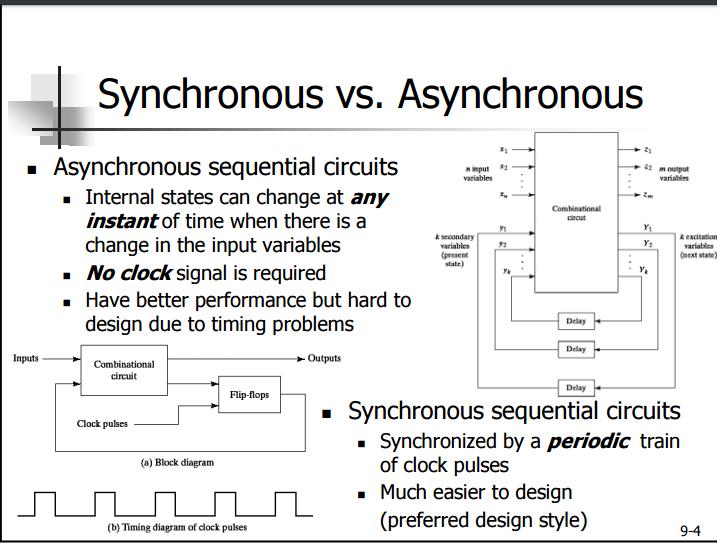
UNIT III. Combinational Circuit- Block Diagram. Sequential Circuit- Block Diagram
 UNIT III INTRODUCTION In combinational logic circuits, the outputs at any instant of time depend only on the input signals present at that time. For a change in input, the output occurs immediately. Combinational
Sequential Circuits. Output depends only and immediately on the inputs Have no memory (dependence on past values of the inputs)
") Sequential Circuits Combinational circuits Output depends only and immediately on the inputs Have no memory (dependence on past values of the inputs) Sequential circuits Combination circuits with memory
Sequential Circuits Combinational circuits Output depends only and immediately on the inputs Have no memory (dependence on past values of the inputs) Sequential circuits Combination circuits with memory
Synchronous Sequential Logic
 Synchronous Sequential Logic ( 范倫達 ), Ph. D. Department of Computer Science National Chiao Tung University Taiwan, R.O.C. Fall, 2012 ldvan@cs.nctu.edu.tw http://www.cs.nctu.edu.tw/~ldvan/ Outlines Sequential
Synchronous Sequential Logic
 Synchronous Sequential Logic ( 范倫達 ), Ph. D. Department of Computer Science National Chiao Tung University Taiwan, R.O.C. Fall, 2017 ldvan@cs.nctu.edu.tw http://www.cs.nctu.edu.tw/~ldvan/ Outlines Sequential
Digital Logic Design I
 Digital Logic Design I Synchronous Sequential Logic Mustafa Kemal Uyguroğlu Sequential Circuits Asynchronous Inputs Combinational Circuit Memory Elements Outputs Synchronous Inputs Combinational Circuit
Chapter. Synchronous Sequential Circuits
 Chapter 5 Synchronous Sequential Circuits Logic Circuits- Review Logic Circuits 2 Combinational Circuits Consists of logic gates whose outputs are determined from the current combination of inputs. Performs
Digital Logic Design Sequential Circuits. Dr. Basem ElHalawany
 Digital Logic Design Sequential Circuits Dr. Basem ElHalawany Combinational vs Sequential inputs X Combinational Circuits outputs Z A combinational circuit: At any time, outputs depends only on inputs
Digital Design, Kyung Hee Univ. Chapter 5. Synchronous Sequential Logic
 Chapter 5. Synchronous Sequential Logic 1 5.1 Introduction Electronic products: ability to send, receive, store, retrieve, and process information in binary format Dependence on past values of inputs Sequential
Unit 11. Latches and Flip-Flops
 Unit 11 Latches and Flip-Flops 1 Combinational Circuits A combinational circuit consists of logic gates whose outputs, at any time, are determined by combining the values of the inputs. For n input variables,
Synchronous Sequential Logic
 MEC520 디지털공학 Synchronous Sequential Logic Jee-Hwan Ryu School of Mechanical Engineering Sequential Circuits Outputs are function of inputs and present states Present states are supplied by memory elements
MC9211 Computer Organization
 MC9211 Computer Organization Unit 2 : Combinational and Sequential Circuits Lesson2 : Sequential Circuits (KSB) (MCA) (2009-12/ODD) (2009-10/1 A&B) Coverage Lesson2 Outlines the formal procedures for the
Other Flip-Flops. Lecture 27 1
 Other Flip-Flops Other types of flip-flops can be constructed by using the D flip-flop and external logic. Two flip-flops less widely used in the design of digital systems are the JK and T flip-flops.
Chapter 5 Synchronous Sequential Logic
 EEA051 - Digital Logic 數位邏輯 Chapter 5 Synchronous Sequential Logic 吳俊興國立高雄大學資訊工程學系 December 2005 Chapter 5 Synchronous Sequential Logic 5-1 Sequential Circuits 5-2 Latches 5-3 Flip-Flops 5-4 Analysis of
Chapter 8 Sequential Circuits
 Philadelphia University Faculty of Information Technology Department of Computer Science Computer Logic Design By 1 Chapter 8 Sequential Circuits 1 Classification of Combinational Logic 3 Sequential circuits
NH 67, Karur Trichy Highways, Puliyur C.F, Karur District UNIT-III SEQUENTIAL CIRCUITS
 NH 67, Karur Trichy Highways, Puliyur C.F, 639 114 Karur District DEPARTMENT OF ELETRONICS AND COMMUNICATION ENGINEERING COURSE NOTES SUBJECT: DIGITAL ELECTRONICS CLASS: II YEAR ECE SUBJECT CODE: EC2203
Lecture 11: Synchronous Sequential Logic
 Lecture 11: Synchronous Sequential Logic Syed M. Mahmud, Ph.D ECE Department Wayne State University Aby K George, ECE Department, Wayne State University Contents Characteristic equations Analysis of clocked
D Latch (Transparent Latch)
") D Latch (Transparent Latch) -One way to eliminate the undesirable condition of the indeterminate state in the SR latch is to ensure that inputs S and R are never equal to 1 at the same time. This is done
D Latch (Transparent Latch) -One way to eliminate the undesirable condition of the indeterminate state in the SR latch is to ensure that inputs S and R are never equal to 1 at the same time. This is done
CHAPTER 4: Logic Circuits
 CHAPTER 4: Logic Circuits II. Sequential Circuits Combinational circuits o The outputs depend only on the current input values o It uses only logic gates, decoders, multiplexers, ALUs Sequential circuits
CHAPTER 4: Logic Circuits
 CHAPTER 4: Logic Circuits II. Sequential Circuits Combinational circuits o The outputs depend only on the current input values o It uses only logic gates, decoders, multiplexers, ALUs Sequential circuits
CSE Latches and Flip-flops Dr. Izadi. NOR gate property: A B Z Cross coupled NOR gates: S M S R Q M
 CSE-4523 Latches and Flip-flops Dr. Izadi NOR gate property: A B Z A B Z Cross coupled NOR gates: S M S R M R S M R S R S R M S S M R R S ' Gate R Gate S R S G R S R (t+) S G R Flip_flops:. S-R flip-flop
Chapter 5 Synchronous Sequential Logic
 Chapter 5 Synchronous Sequential Logic Chih-Tsun Huang ( 黃稚存 ) http://nthucad.cs.nthu.edu.tw/~cthuang/ Department of Computer Science National Tsing Hua University Outline Introduction Storage Elements:
CS T34-DIGITAL SYSTEM DESIGN Y2/S3
 UNIT III Sequential Logic: Latches versus Flip Flops SR, D, JK, Master Slave Flip Flops Excitation table Conversion of Flip flops Counters: Asynchronous, synchronous, decade, presettable Shift Registers:
Chapter 5. Introduction
 Chapter 5 Synchronous Sequential Logic Chapter 5 Introduction Circuits require memory to store intermediate data Sequential circuits use a periodic signal to determine when to store values. A clock signal
ELCT201: DIGITAL LOGIC DESIGN
 ELCT201: DIGITAL LOGIC DESIGN Dr. Eng. Haitham Omran, haitham.omran@guc.edu.eg Dr. Eng. Wassim Alexan, wassim.joseph@guc.edu.eg Lecture 8 Following the slides of Dr. Ahmed H. Madian محرم 1439 ه Winter
Synchronous Sequential Logic
 Synchronous Sequential Logic Ranga Rodrigo August 2, 2009 1 Behavioral Modeling Behavioral modeling represents digital circuits at a functional and algorithmic level. It is used mostly to describe sequential
ELE2120 Digital Circuits and Systems. Tutorial Note 7
 ELE2120 Digital Circuits and Systems Tutorial Note 7 Outline 1. Sequential Circuit 2. Gated SR Latch 3. Gated D-latch 4. Edge-Triggered D Flip-Flop 5. Asynchronous and Synchronous reset Sequential Circuit
CHAPTER1: Digital Logic Circuits
 CS224: Computer Organization S.KHABET CHAPTER1: Digital Logic Circuits 1 Sequential Circuits Introduction Composed of a combinational circuit to which the memory elements are connected to form a feedback
ELCT201: DIGITAL LOGIC DESIGN
 ELCT201: DIGITAL LOGIC DESIGN Dr. Eng. Haitham Omran, haitham.omran@guc.edu.eg Dr. Eng. Wassim Alexan, wassim.joseph@guc.edu.eg Lecture 7 Following the slides of Dr. Ahmed H. Madian محرم 1439 ه Winter
Synchronous Sequential Logic
 Synchronous Sequential Logic -A Sequential Circuit consists of a combinational circuit to which storage elements are connected to form a feedback path. The storage elements are devices capable of storing
NH 67, Karur Trichy Highways, Puliyur C.F, Karur District DEPARTMENT OF INFORMATION TECHNOLOGY CS 2202 DIGITAL PRINCIPLES AND SYSTEM DESIGN
 NH 67, Karur Trichy Highways, Puliyur C.F, 639 114 Karur District DEPARTMENT OF INFORMATION TECHNOLOGY CS 2202 DIGITAL PRINCIPLES AND SYSTEM DESIGN UNIT 4 SYNCHRONOUS SEQUENTIAL LOGIC Sequential circuits
`COEN 312 DIGITAL SYSTEMS DESIGN - LECTURE NOTES Concordia University
 `OEN 32 IGITL SYSTEMS ESIGN - LETURE NOTES oncordia University hapter 5: Synchronous Sequential Logic NOTE: For more eamples and detailed description of the material in the lecture notes, please refer
Chapter 5 Sequential Circuits
 Logic and Computer Design Fundamentals Chapter 5 Sequential Circuits Part 2 Sequential Circuit Design Charles Kime & Thomas Kaminski 28 Pearson Education, Inc. (Hyperlinks are active in View Show mode)
The word digital implies information in computers is represented by variables that take a limited number of discrete values.
 Class Overview Cover hardware operation of digital computers. First, consider the various digital components used in the organization and design. Second, go through the necessary steps to design a basic
Logic and Computer Design Fundamentals. Chapter 7. Registers and Counters
 Logic and Computer Design Fundamentals Chapter 7 Registers and Counters Registers Register a collection of binary storage elements In theory, a register is sequential logic which can be defined by a state
Combinational / Sequential Logic
 Digital Circuit Design and Language Combinational / Sequential Logic Chang, Ik Joon Kyunghee University Combinational Logic + The outputs are determined by the present inputs + Consist of input/output
Flip-Flops. Because of this the state of the latch may keep changing in circuits with feedback as long as the clock pulse remains active.
 Flip-Flops Objectives The objectives of this lesson are to study: 1. Latches versus Flip-Flops 2. Master-Slave Flip-Flops 3. Timing Analysis of Master-Slave Flip-Flops 4. Different Types of Master-Slave
Logic Design. Flip Flops, Registers and Counters
 Logic Design Flip Flops, Registers and Counters Introduction Combinational circuits: value of each output depends only on the values of inputs Sequential Circuits: values of outputs depend on inputs and
ELCT201: DIGITAL LOGIC DESIGN
 ELCT201: DIGITAL LOGIC DESIGN Dr. Eng. Haitham Omran, haitham.omran@guc.edu.eg Dr. Eng. Wassim Alexan, wassim.joseph@guc.edu.eg Lecture 6 Following the slides of Dr. Ahmed H. Madian ذو الحجة 1438 ه Winter
Experiment 8 Introduction to Latches and Flip-Flops and registers
 Experiment 8 Introduction to Latches and Flip-Flops and registers Introduction: The logic circuits that have been used until now were combinational logic circuits since the output of the device depends
Chapter 6. Flip-Flops and Simple Flip-Flop Applications
 Chapter 6 Flip-Flops and Simple Flip-Flop Applications Basic bistable element It is a circuit having two stable conditions (states). It can be used to store binary symbols. J. C. Huang, 2004 Digital Logic
Chapter 5 Sequential Circuits
 Logic and omputer Design Fundamentals hapter 5 Sequential ircuits Part 1 Storage Elements and Sequential ircuit Analysis harles Kime & Thomas Kaminski 2008 Pearson Education, Inc. (Hyperlinks are active
Analysis of Clocked Sequential Circuits
 Analysis of Clocked Sequential Circuits COE 202 Digital Logic Design Dr. Muhamed Mudawar King Fahd University of Petroleum and Minerals Presentation Outline Analysis of Clocked Sequential circuits State
COE 202: Digital Logic Design Sequential Circuits Part 1. Dr. Ahmad Almulhem ahmadsm AT kfupm Phone: Office:
 COE 202: Digital Logic Design Sequential Circuits Part 1 Dr. Ahmad Almulhem Email: ahmadsm AT kfupm Phone: 860-7554 Office: 22-324 Objectives Sequential Circuits Memory Elements Latches Flip-Flops Combinational
Vignana Bharathi Institute of Technology UNIT 4 DLD
 DLD UNIT IV Synchronous Sequential Circuits, Latches, Flip-flops, analysis of clocked sequential circuits, Registers, Shift registers, Ripple counters, Synchronous counters, other counters. Asynchronous
ECE 341. Lecture # 2
 ECE 341 Lecture # 2 Instructor: Zeshan Chishti zeshan@pdx.edu October 1, 2014 Portland State University Announcements Course website reminder: http://www.ece.pdx.edu/~zeshan/ece341.htm Homework 1: Will
Introduction to Sequential Circuits
 Introduction to Sequential Circuits COE 202 Digital Logic Design Dr. Muhamed Mudawar King Fahd University of Petroleum and Minerals Presentation Outline Introduction to Sequential Circuits Synchronous
Chapter 5 Synchronous Sequential Logic
 Chapter 5 Synchronous Sequential Logic Sequential Circuits Latches and Flip-Flops Analysis of Clocked Sequential Circuits HDL Optimization Design Procedure Sequential Circuits Various definitions Combinational
Lecture 12. Amirali Baniasadi
 CENG 24 Digital Design Lecture 2 Amirali Baniasadi amirali@ece.uvic.ca This Lecture Chapter 6: Registers and Counters 2 Registers Sequential circuits are classified based in their function, e.g., registers.
MODULE 3. Combinational & Sequential logic
 MODULE 3 Combinational & Sequential logic Combinational Logic Introduction Logic circuit may be classified into two categories. Combinational logic circuits 2. Sequential logic circuits A combinational
Sequential Digital Design. Laboratory Manual. Experiment #3. Flip Flop Storage Elements
 The Islamic University of Gaza Engineering Faculty Department of Computer Engineering Spring 2018 ECOM 2022 Khaleel I. Shaheen Sequential Digital Design Laboratory Manual Experiment #3 Flip Flop Storage
EMT 125 Digital Electronic Principles I CHAPTER 6 : FLIP-FLOP
 EMT 125 Digital Electronic Principles I CHAPTER 6 : FLIP-FLOP 1 Chapter Overview Latches Gated Latches Edge-triggered flip-flops Master-slave flip-flops Flip-flop operating characteristics Flip-flop applications
RS flip-flop using NOR gate
 RS flip-flop using NOR gate Triggering and triggering methods Triggering : Applying train of pulses, to set or reset the memory cell is known as Triggering. Triggering methods:- There are basically two
EE292: Fundamentals of ECE
 EE292: Fundamentals of ECE Fall 2012 TTh 10:00-11:15 SEB 1242 Lecture 23 121120 http://www.ee.unlv.edu/~b1morris/ee292/ 2 Outline Review Combinatorial Logic Sequential Logic 3 Combinatorial Logic Circuits
Combinational vs Sequential
 Combinational vs Sequential inputs X Combinational Circuits outputs Z A combinational circuit: At any time, outputs depends only on inputs Changing inputs changes outputs No regard for previous inputs
Flip-Flops and Sequential Circuit Design
 Flip-Flops and Sequential Circuit Design ECE 52 Summer 29 Reading ssignment Brown and Vranesic 7 Flip-Flops, Registers, Counters and a Simple Processor 7.5 T Flip-Flop 7.5. Configurable Flip-Flops 7.6
Digital Circuit And Logic Design I. Lecture 8
 Digital Circuit And Logic Design I Lecture 8 Outline Sequential Logic Design Principles (1) 1. Introduction 2. Latch and Flip-flops 3. Clocked Synchronous State-Machine Analysis Panupong Sornkhom, 2005/2
Digital Circuit And Logic Design I
 Digital Circuit And Logic Design I Lecture 8 Outline Sequential Logic Design Principles (1) 1. Introduction 2. Latch and Flip-flops 3. Clocked Synchronous State-Machine Panupong Sornkhom, 2005/2 2 1 Sequential
Chapter 4. Logic Design
 Chapter 4 Logic Design 4.1 Introduction. In previous Chapter we studied gates and combinational circuits, which made by gates (AND, OR, NOT etc.). That can be represented by circuit diagram, truth table
The reduction in the number of flip-flops in a sequential circuit is referred to as the state-reduction problem.
 State Reduction The reduction in the number of flip-flops in a sequential circuit is referred to as the state-reduction problem. State-reduction algorithms are concerned with procedures for reducing the
Department of CSIT. Class: B.SC Semester: II Year: 2013 Paper Title: Introduction to logics of Computer Max Marks: 30
 Department of CSIT Class: B.SC Semester: II Year: 2013 Paper Title: Introduction to logics of Computer Max Marks: 30 Section A: (All 10 questions compulsory) 10X1=10 Very Short Answer Questions: Write
ELE2120 Digital Circuits and Systems. Tutorial Note 8
 ELE2120 Digital Circuits and Systems Tutorial Note 8 Outline 1. Register 2. Counters 3. Synchronous Counter 4. Asynchronous Counter 5. Sequential Circuit Design Overview 1. Register Applications: temporally
LAB 7. Latches & Flip Flops
 بسام عب د الكريم جاد هللا النبريص Bass am Ak J Alnabr iss Islamic University of Gaza Faculty of Engineering Computer Engineering Dept. Digital Design Lab : ECOM 2112 Fall 2016 Eng. Bassam Nabriss LAB 7
Chapter 3 Unit Combinational
 EE 2: igital Logic ircuit esign r Radwan E Abdel-Aal, OE Logic and omputer esign Fundamentals hapter 3 Unit ombinational 4 Sequential Logic esign ircuits Part Implementation Technology and Logic esign
Figure 30.1a Timing diagram of the divide by 60 minutes/seconds counter
 Digital Clock The timing diagram figure 30.1a shows the time interval t 6 to t 11 and t 19 to t 21. At time interval t 9 the units counter counts to 1001 (9) which is the terminal count of the 74x160 decade
Module -5 Sequential Logic Design
 Module -5 Sequential Logic Design 5.1. Motivation: In digital circuit theory, sequential logic is a type of logic circuit whose output depends not only on the present value of its input signals but on
Final Exam review: chapter 4 and 5. Supplement 3 and 4
 Final Exam review: chapter 4 and 5. Supplement 3 and 4 1. A new type of synchronous flip-flop has the following characteristic table. Find the corresponding excitation table with don t cares used as much
1. Convert the decimal number to binary, octal, and hexadecimal.
 1. Convert the decimal number 435.64 to binary, octal, and hexadecimal. 2. Part A. Convert the circuit below into NAND gates. Insert or remove inverters as necessary. Part B. What is the propagation delay
ECE 25 Introduction to Digital Design. Chapter 5 Sequential Circuits ( ) Part 1 Storage Elements and Sequential Circuit Analysis
 Part 1 Storage Elements and Sequential Circuit Analysis") EE 25 Introduction to igital esign hapter 5 Sequential ircuits (5.1-5.4) Part 1 Storage Elements and Sequential ircuit Analysis Logic and omputer esign Fundamentals harles Kime & Thomas Kaminski 2008 Pearson
EE 25 Introduction to igital esign hapter 5 Sequential ircuits (5.1-5.4) Part 1 Storage Elements and Sequential ircuit Analysis Logic and omputer esign Fundamentals harles Kime & Thomas Kaminski 2008 Pearson
Course Administration
 EE 224: INTRODUCTION TO DIGITAL CIRCUITS & COMPUTER DESIGN Lecture 5: Sequential Logic - 2 Analysis of Clocked Sequential Systems 4/2/2 Avinash Kodi, kodi@ohio.edu Course Administration 2 Hw 2 due on today
Registers and Counters
 Registers and Counters Clocked sequential circuit = F/Fs and combinational gates Register Group of flip-flops (share a common clock and capable of storing one bit of information) Consist of a group of
(CSC-3501) Lecture 7 (07 Feb 2008) Seung-Jong Park (Jay) CSC S.J. Park. Announcement
 Lecture 7 (07 Feb 2008) Seung-Jong Park (Jay) CSC S.J. Park. Announcement") Seung-Jong Park (Jay) http://www.csc.lsu.edu/~sjpark Computer Architecture (CSC-3501) Lecture 7 (07 Feb 2008) 1 Announcement 2 1 Combinational vs. Sequential Logic Combinational Logic Memoryless Outputs
Seung-Jong Park (Jay) http://www.csc.lsu.edu/~sjpark Computer Architecture (CSC-3501) Lecture 7 (07 Feb 2008) 1 Announcement 2 1 Combinational vs. Sequential Logic Combinational Logic Memoryless Outputs
YEDITEPE UNIVERSITY DEPARTMENT OF COMPUTER ENGINEERING. EXPERIMENT VIII: FLIP-FLOPS, COUNTERS 2014 Fall
 YEDITEPE UNIVERSITY DEPARTMENT OF COMPUTER ENGINEERING EXPERIMENT VIII: FLIP-FLOPS, COUNTERS 2014 Fall Objective: - Dealing with the operation of simple sequential devices. Learning invalid condition in
LAB #4 SEQUENTIAL LOGIC CIRCUIT
 LAB #4 SEQUENTIAL LOGIC CIRCUIT OBJECTIVES 1. To learn how basic sequential logic circuit works 2. To test and investigate the operation of various latch and flip flop circuits INTRODUCTIONS Sequential
Digital Logic Design ENEE x. Lecture 19
 Digital Logic Design ENEE 244-010x Lecture 19 Announcements Homework 8 due on Monday, 11/23. Agenda Last time: Timing Considerations (6.3) Master-Slave Flip-Flops (6.4) This time: Edge-Triggered Flip-Flops
 WWW.STUDENTSFOCUS.COM + Class Subject Code Subject Prepared By Lesson Plan for Time: Lesson. No 1.CONTENT LIST: Introduction to Unit III 2. SKILLS ADDRESSED: Listening I year, 02 sem CS6201 Digital Principles
UNIT IV. Sequential circuit
 UNIT IV Sequential circuit Introduction In the previous session, we said that the output of a combinational circuit depends solely upon the input. The implication is that combinational circuits have no
Problems with D-Latch
 Problems with -Latch If changes while is true, the new value of will appear at the output. The latch is transparent. If the stored value can change state more than once during a single clock pulse, the
2 Sequential Circuits
 2 2.1 State Diagrams and General Form 0/0 1/0 Start State 0 /0 1/1 State 1 /1 0/1 State Diagram of a Change Detector ( Mealy-machine). The output Y assumes 1 whenever the input X has changed. Otherwise
RS flip-flop using NOR gate
 RS flip-flop using NOR gate Triggering and triggering methods Triggering : Applying train of pulses, to set or reset the memory cell is known as Triggering. Triggering methods:- There are basically two
CS302 - Digital Logic Design FAQs By
 CS302 - Digital Logic Design FAQs By For BCD numbers that add up to an invalid BCD number or generate a carry the number 6 (0110) is added to the invalid number, why? These binary numbers are not allowed
MODU LE DAY. Class-A, B, AB and C amplifiers - basic concepts, power, efficiency Basic concepts of Feedback and Oscillation. Day 1
 DAY MODU LE TOPIC QUESTIONS Day 1 Day 2 Day 3 Day 4 I Class-A, B, AB and C amplifiers - basic concepts, power, efficiency Basic concepts of Feedback and Oscillation Phase Shift Wein Bridge oscillators.
To design a sequential logic circuit using D-Flip-flop. To implement the designed circuit.
 6.1 Objectives To design a sequential logic circuit using D-Flip-flop. To implement the designed circuit. 6.2 Sequential Logic So far we have implemented digital circuits whose outputs depend only on its
Solution to Digital Logic )What is the magnitude comparator? Design a logic circuit for 4 bit magnitude comparator and explain it,
What is the magnitude comparator? Design a logic circuit for 4 bit magnitude comparator and explain it,") Solution to Digital Logic -2067 Solution to digital logic 2067 1.)What is the magnitude comparator? Design a logic circuit for 4 bit magnitude comparator and explain it, A Magnitude comparator is a combinational
Solution to Digital Logic -2067 Solution to digital logic 2067 1.)What is the magnitude comparator? Design a logic circuit for 4 bit magnitude comparator and explain it, A Magnitude comparator is a combinational
Engr354: Digital Logic Circuits
 Engr354: igital Circuits Chapter 7 Sequential Elements r. Curtis Nelson Sequential Elements In this chapter you will learn about: circuits that can store information; Basic cells, latches, and flip-flops;
 UNIT 1 NUMBER SYSTEMS AND DIGITAL LOGIC FAMILIES 1. Briefly explain the stream lined method of converting binary to decimal number with example. 2. Give the Gray code for the binary number (111) 2. 3.
CS8803: Advanced Digital Design for Embedded Hardware
 CS883: Advanced Digital Design for Embedded Hardware Lecture 4: Latches, Flip-Flops, and Sequential Circuits Instructor: Sung Kyu Lim (limsk@ece.gatech.edu) Website: http://users.ece.gatech.edu/limsk/course/cs883
Sequential Logic. E&CE 223 Digital Circuits and Systems (A. Kennings) Page 1
 Page 1") Sequential Logic E&CE 223 igital Circuits and Systems (A. Kennings) Page 1 Sequential Circuits Have considered only combinational circuits in which circuit outputs are determined entirely by current circuit
Sequential Logic E&CE 223 igital Circuits and Systems (A. Kennings) Page 1 Sequential Circuits Have considered only combinational circuits in which circuit outputs are determined entirely by current circuit
DIGITAL SYSTEM FUNDAMENTALS (ECE421) DIGITAL ELECTRONICS FUNDAMENTAL (ECE422) COUNTERS
 DIGITAL ELECTRONICS FUNDAMENTAL (ECE422) COUNTERS") COURSE / CODE DIGITAL SYSTEM FUNDAMENTALS (ECE421) DIGITAL ELECTRONICS FUNDAMENTAL (ECE422) COUNTERS One common requirement in digital circuits is counting, both forward and backward. Digital clocks and
COURSE / CODE DIGITAL SYSTEM FUNDAMENTALS (ECE421) DIGITAL ELECTRONICS FUNDAMENTAL (ECE422) COUNTERS One common requirement in digital circuits is counting, both forward and backward. Digital clocks and
Asynchronous (Ripple) Counters
 Counters") Circuits for counting events are frequently used in computers and other digital systems. Since a counter circuit must remember its past states, it has to possess memory. The chapter about flip-flops introduced
Circuits for counting events are frequently used in computers and other digital systems. Since a counter circuit must remember its past states, it has to possess memory. The chapter about flip-flops introduced
Logic Design II (17.342) Spring Lecture Outline
 Spring Lecture Outline") Logic Design II (17.342) Spring 2012 Lecture Outline Class # 05 February 23, 2012 Dohn Bowden 1 Today s Lecture Analysis of Clocked Sequential Circuits Chapter 13 2 Course Admin 3 Administrative Admin
Logic Design II (17.342) Spring 2012 Lecture Outline Class # 05 February 23, 2012 Dohn Bowden 1 Today s Lecture Analysis of Clocked Sequential Circuits Chapter 13 2 Course Admin 3 Administrative Admin
Sequential Logic and Clocked Circuits
 Sequential Logic and Clocked Circuits Clock or Timing Device Input Variables State or Memory Element Combinational Logic Elements From combinational logic, we move on to sequential logic. Sequential logic
11.1 As mentioned in Experiment 10, sequential logic circuits are a type of logic circuit where the output
 EE 2449 Experiment JL and NWP //8 CALIFORNIA STATE UNIVERSITY LOS ANGELES Department of Electrical and Computer Engineering EE-2449 Digital Logic Lab EXPERIMENT SEQUENTIAL CIRCUITS Text: Mano and Ciletti,
Registers and Counters
 Registers and Counters Clocked sequential circuit = F/Fs and combinational gates Register Group of flip-flops (share a common clock and capable of storing one bit of information) Consist of a group of
DIGITAL CIRCUIT LOGIC UNIT 11: SEQUENTIAL CIRCUITS (LATCHES AND FLIP-FLOPS)
") DIGITAL CIRCUIT LOGIC UNIT 11: SEQUENTIAL CIRCUITS (LATCHES AND FLIP-FLOPS) 1 iclicker Question 16 What should be the MUX inputs to implement the following function? (4 minutes) f A, B, C = m(0,2,5,6,7)
DIGITAL CIRCUIT LOGIC UNIT 11: SEQUENTIAL CIRCUITS (LATCHES AND FLIP-FLOPS) 1 iclicker Question 16 What should be the MUX inputs to implement the following function? (4 minutes) f A, B, C = m(0,2,5,6,7)
Chapter 3. Boolean Algebra and Digital Logic
 Chapter 3 Boolean Algebra and Digital Logic Chapter 3 Objectives Understand the relationship between Boolean logic and digital computer circuits. Learn how to design simple logic circuits. Understand how
EKT 121/4 ELEKTRONIK DIGIT 1
 EKT 2/4 ELEKTRONIK DIGIT Kolej Universiti Kejuruteraan Utara Malaysia Sequential Logic Circuits - COUNTERS - LATCHES (review) S-R R Latch S-R R Latch Active-LOW input INPUTS OUTPUTS S R Q Q COMMENTS Q