Advances in Roll-to-Roll Imprint Lithography for Display Applications Using Self Aligned Imprint Lithography. John G Maltabes HP Labs
|
|
|
- Oliver Manning
- 5 years ago
- Views:
Transcription
1 Advances in Roll-to-Roll Imprint Lithography for Display Applications Using Self Aligned Imprint Lithography John G Maltabes HP Labs
2 Outline Introduction Roll to Roll Challenges and Benefits HP Labs Roll to Roll SAIL process overview Current toolset and methods Initial R2R demonstrators Transitioning to Manufacturing Internal work Still needed Call for Standards Summary
3 Introduction HP Labs has developed a process for TFT flexible display backplanes TFT film stack deposition done by PowerFilm Solar in Ames IA All patterning, etch and testing done in HP Labs Process routinely yields workable devices Strong desire by both HP and PowerFilm to move from Lab Project to Manufacturing
4 Challenges & Benefits of R2R Electronics Fabrication Benefits Challenges Lower substrate cost Steady state processing: high-throughput, high yield Lower cleanroom requirements Cheaper equipment - better scaling? Lower process temperature Defect repair patterning Limited equipment available no previous generation


5 R2R SAIL Process Flow Vacuum deposition of metals, dielectrics, & semiconductors deposition Multiple mask levels imprinted as single 3D structure imprint 20 m etch Patterning completed w/ wet & dry processes


6 SAIL process: Imprinting Coating Station Imprinting Station Imprinted web Imprinting roller with elastomeric stamp Supply Pixel speed depends linearly on mobility but inversely with the square of channel length Take-Up Imprinted web High resolution 40 nm line width High aspect ratio & multiple step heights sub-micron features with 4 levels and 5:1 aspect ratio House-built R2R coating & imprinting machine (throughput rate = 0.5~5 m/min)
7 Imprint Lithography is the Best Choice for R2R Patterning Photolithography Imprint lithography Inkjet Physical mask Laser ablation Throughput Moderate: limited by step & repeat / stitching High: > 5 meters/min Low Limited only by deposition Low Resolution Limited by substrate flatness ~10μ 100nm demonstrated >10μ 10μ -100μ ~10μ Alignment Limited by substrate flatness ~10μ Self alignment possible External sensor required poor ~10μ Issues Scaling to large areas costly New technology Materials must be jettable Cleaning, particles Thermal effects, selectivity


8 PDMS Copies of Master Wafer Liquid PDMS on patterned wafer. Trimmed PDMS stamp.


9 Imprint Roller Fabrication Full-size shim for roller cover. Finished imprint rollers.

10 1/3m Coater/Imprinter in Operation

11 1/3 m R2R Coater/Imprinter Supply Web Cleaner Gravure Coater Imprinter Take-up Slide caption


12 R2R RIE 1/3m wide web; 6 core Up to 3 inline etch zones (1 currently) Chlorine compatible system Currently fluorine based chemistries: CHF 3, CF 4, SF 6, Ar, N 2, O 2 for polymer and Si etching Web grounded to temp controlled electrode vision system for microscopy or endpoint control
13 Current R2R Tool Summary 330mm wide web; 6 core Either vacuum or class 100 enclosures Metal PECVD Imprint Wet Etch RIE Cleaning 13 sputter or evaporation multiple inline targets simultaneous front/back coating no sliding contact 13 production solar cell or 13 drum coater (no sliding contact optimized for TFT materials 13 gravure coater cure through stamp and quartz roller large format masters (A4) 13 enclosed, clean system front side protection acid based processes for Cr and Al with inspection 13 system integrated tacky roller system cleaning in imprinter


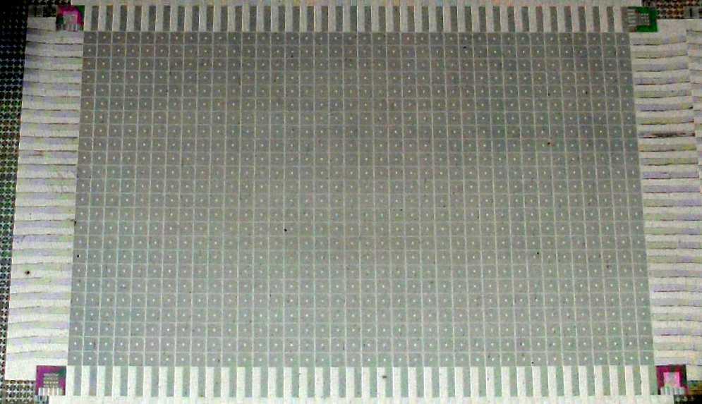
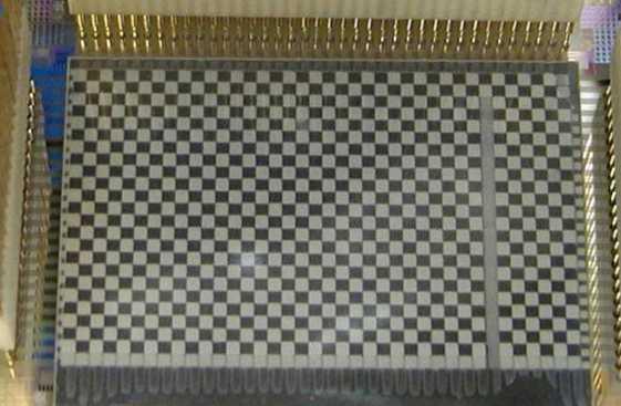
14 Initial display demonstrators SAIL Backplane on flexible substrate World s first active matrix display made exclusively with R2R processes (including E Ink Front Plane)


15 Transition from lab to Manufacturing Internal activities Instituted tracking of all web processing Implemented a MES system Testing TFT stack webs from PowerFilm for conformance to spec Developed a web marking methodology using 2D Data matrix codes written on the edge of the web for real time process tracking through tools


16 Transition from lab to Manufacturing Stamp (roller) lifetime transition from PDMS Amorphous fluorocarbons have demonstrated good durability Goal : 1 KM imprint/roller Imprint #25 Imprint #2500
17 Still needed Higher quality substrates Lower particulates, clean from manufacturer Better control of center to edge finish Master roll ~ 1meter wide, slit into 1/3 meter widths Inspection tools for both patterned and unpatterned webs CAMM working on unpatterned measurements HP has done some initial work with Rudolph Technology on patterned inspection
18 Still needed Etched quartz imprint rollers Polymer approach is great for prototyping or short runs High volume long runs will need a more durable master Existing mask making tools can be adapted for this application - High NRE costs Test equipment and methods compatible with R2R manufacturing
19 Standards Standards would allow unified specification to both material suppliers and equipment suppliers Would allow for faster development of products and processes, higher yields and ultimately lower cost Approach work on common items Materials Width, roll lengths, identification marks, particles Inspection Lithography - Imprint and projection
20 Summary R2R manufacturing of electronics on flexible substrates is feasible and will be cost effective Basic materials, processes, and architectures have been demonstrated more work remains to be done to improve yield and scaling Complete toolset for R2R processing capable of pilot production Standards for web materials and tool sets will open up more choices as we move to high volume manufacturing

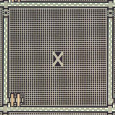
21 Sail Backplane Demo
Enabling Paper-Like Displays Roll-to-Roll Manufacturing of Display Backplanes. Hewlett-Packard Company, Palo Alto, CA. Phicot Inc, Ames, IA
 Enabling Paper-Like Displays Roll-to-Roll Manufacturing of Display Backplanes Carl Taussig, Bob Cobene, Rich Elder, Warren Jackson, Mehrban Jam, Albert Jeans, Hao Luo, Ping Mei, Craig Perlov, Hewlett-Packard
Defect Analysis of Roll-to-Roll SAIL Manufactured Flexible Display Backplanes
 Defect Analysis of Roll-to-Roll SAIL Manufactured Flexible Display Backplanes Carl Taussig, Richard E. Elder, Warren B. Jackson, Albert Jeans, Mehrban Jam, Ed Holland, Hao Luo, John Maltabes, Craig Perlov,
Flexible Electronics Production Deployment on FPD Standards: Plastic Displays & Integrated Circuits. Stanislav Loboda R&D engineer
 Flexible Electronics Production Deployment on FPD Standards: Plastic Displays & Integrated Circuits Stanislav Loboda R&D engineer The world-first small-volume contract manufacturing for plastic TFT-arrays
UV Nanoimprint Tool and Process Technology. S.V. Sreenivasan December 13 th, 2007
 UV Nanoimprint Tool and Process Technology S.V. Sreenivasan December 13 th, 2007 Agenda Introduction Need tool and process technology that can address: Patterning and CD control Alignment and Overlay Defect
Advanced Display Manufacturing Technology
 Advanced Display Manufacturing Technology John Busch Vice President, New Business Development Display and Flexible Technology Group September 28, 2017 Safe Harbor This presentation contains forward-looking
1. Publishable summary
 1. Publishable summary 1.1. Project objectives. The target of the project is to develop a highly reliable high brightness conformable low cost scalable display for demanding applications such as their
Industrial Inline Control for Advanced Vacuum Roll to Roll Systems. Gerhard Steiniger Web inspection - surface Quallity control 7.
 Industrial Inline Control for Advanced Vacuum Roll to Roll Systems Gerhard Steiniger Web inspection - surface Quallity control 7.4-7684 1 Industrial Inline Control for Advanced Vacuum Roll to Roll Systems
HB LEDs & OLEDs. Complete thin film process solutions
 HB LEDs & OLEDs Complete thin film process solutions Get off to a flying start for all your LED thin film deposition and etch processes From 2 inch to 8 inch Manual or fully automated substrate handling
Scalable self-aligned active matrix IGZO TFT backplane technology and its use in flexible semi-transparent image sensors. Albert van Breemen
 Scalable self-aligned active matrix IGZO TFT backplane technology and its use in flexible semi-transparent image sensors Albert van Breemen Image sensors today 1 Dominated by silicon based technology on
PROCESS TECHNOLOGIES FOR ADVANCED ORGANIC ELECTRONIC DEVICES: MICRODISPLAYS, LIGHTING AND SOLAR CELLS
 PROCESS TECHNOLOGIES FOR ADVANCED ORGANIC ELECTRONIC DEVICES: MICRODISPLAYS, LIGHTING AND SOLAR CELLS Dr. Christian May Fraunhofer IPMS - Center for Organic Materials and Electronic Devices Dresden COMEDD
Nano-Imprint Lithography Infrastructure: Imprint Templates
 Nano-Imprint Lithography Infrastructure: Imprint Templates John Maltabes Photronics, Inc Austin, TX 1 Questions to keep in mind Imprint template manufacturability Resolution Can you get sub30nm images?
RTNN Etch capabilities
 RTNN Etch capabilities A Partnership Between NC State University, Duke University, and UNC Chapel Hill Trion Minilock II: III-V RIE Trion Phantom II: Oxide/Nitride/Polymer SPTS Pegasus DRIE Trion Minilock
AIXTRON in EXCILIGHT project
 AIXTRON SE AIXTRON in EXCILIGHT project Gintautas Simkus ABOUT AIXTRON 2 Who we are Headquarter based in Herzogenrath, Germany Worldwide presence with 14 sales/representatives offices and production facilities
TipatOr. Liquid metal switch (LMS) display technology. Avi Fogel
 display technology. Avi Fogel") TipatOr Liquid metal switch (LMS) display technology Avi Fogel 972-52-5702938 avifog@gmail.com Who is behind TipatOr TipatOr emerged from a merger of 2 expert groups in the fields of MEMS and Displays
TipatOr Liquid metal switch (LMS) display technology Avi Fogel 972-52-5702938 avifog@gmail.com Who is behind TipatOr TipatOr emerged from a merger of 2 expert groups in the fields of MEMS and Displays
Overcoming Challenges in 3D NAND Volume Manufacturing
 Overcoming Challenges in 3D NAND Volume Manufacturing Thorsten Lill Vice President, Etch Emerging Technologies and Systems Flash Memory Summit 2017, Santa Clara 2017 Lam Research Corp. Flash Memory Summit
AMOLED Manufacturing Process Report SAMPLE
 AMOLED Manufacturing Process Report SAMPLE 2018 AMOLED Manufacturing Process Report The report analyzes the structure and manufacturing process by dividing AMOLED into small & medium-sized rigid OLED,
Solution-based transistor matrix
 18 PRINTED ELECTRONICS Solution-based transistor matrix A groundbreaking new technology is making it far more cost-effective to produce the electronic control unit of liquid crystal displays. At the same
Defect Reduction for Semiconductor Memory Applications Using Jet And Flash Imprint Lithography
 Defect Reduction for Semiconductor Memory Applications Using Jet And Flash Imprint Lithography Zhengmao Ye, Kang Luo, Xiaoming Lu, Brian Fletcher, Weijun Liu, Frank Xu, Dwayne LaBrake, Douglas Resnick,
The Challenges in Making NIL Master Templates
 The Challenges in Making NIL Master Templates Naoya Hayashi Dai Nippon Printing Co., Ltd. A Member of the ebeam Initiative 2011 Dai Nippon Printing Co.,Ltd. All Rights Reserved. OUTLINE Recent Progress
EQUIPMENT COATING SYSTEMS FOR THIN-FILM PV THIN-FILM PHOTOVOLTAICS. SCALA VISS PIA nova GC120VCR XENIA
 THIN-FILM PHOTOVOLTAICS EQUIPMENT COATING SYSTEMS FOR THIN-FILM PV SCALA VISS PIA nova GC120VCR XENIA OUR STORY. OUR EXPERIENCE. RANGE OF APPLICATIONS VON ARDENNE provides advanced PVD coating equipment
ORGANIC ELECTRONICS PROCESS DEVELOPMENT AND ENCAPSULATION TECHNOLOGIES
 FRAUNHOFER INSTITUTE FOR ORGANIC ELECTRONICS, ELECTRON BEAM AND PLASMA TECHNOLOGY FEP ORGANIC ELECTRONICS PROCESS DEVELOPMENT AND ENCAPSULATION TECHNOLOGIES 2 PROFILE Fraunhofer FEP combines research and
Development of OLED Lighting Applications Using Phosphorescent Emission System
 Development of OLED Lighting Applications Using Phosphorescent Emission System Kazuhiro Oikawa R&D Department OLED Lighting Business Center KONICA MINOLTA ADVANCED LAYERS, INC. October 10, 2012 Outline
R2R Processing of Flexible Devices
 R2R Processing of Flexible Devices Mani Thothadri, PhD Senior Director, New Business & Strategic Initiatives Display & Flexible Technologies Group Flextech June 20, 2017 Acknowledgements Dan Forster Christoph
Zeon PDF Driver Trial
 OLED Technology and Product Development in RiTdisplay Chorng-Shyr Jou RiTdisplay csjou@ritdisplay.com 1 Contents I. The Technologies & Challenge of OLED II. The Application of OLED III.Who are Working
Self-Aligned Double Patterning for 3xnm Flash Production
 Self-Aligned Double Patterning for 3xnm Flash Production Chris Ngai Dir of Process Engineering & Lithography Maydan Technology Center Group Applied Materials, Inc. July 16 th, 2008 Overview Double Patterning
Wafer Thinning and Thru-Silicon Vias
 Wafer Thinning and Thru-Silicon Vias The Path to Wafer Level Packaging jreche@trusi.com Summary A new dry etching technology Atmospheric Downstream Plasma (ADP) Etch Applications to Packaging Wafer Thinning
New Worlds for Polymers: Organic Transistors, Light Emitting Diodes, and Optical Waveguides Ed Chandross
 New Worlds for Polymers: Organic Transistors, Light Emitting Diodes, and Optical Waveguides Ed Chandross Materials Chemistry, LLC 1 Polymers in the Electronic Industry Enabling Materials Active Materials?
THE NEXT LEVEL IN ARCHITECTURAL GLASS COATING ADVANCED EQUIPMENT & PROCESS EXPERTISE ADVANCED EQUIPMENT & PROCESS EXPERTISE
 THE NEXT LEVEL IN ARCHITECTURAL GLASS COATING ADVANCED EQUIPMENT & PROCESS EXPERTISE THE NEXT LEVEL IN ARCHITECTURAL GLASS COATING ADVANCED EQUIPMENT & PROCESS EXPERTISE ARCHITECTURAL GLASS COATING REACHES
The Flat Panel Display Paradigm: Successful Implementation of Microelectronic Processes on Gigantic Wafers
 The Flat Panel Display Paradigm: Successful Implementation of Microelectronic Processes on Gigantic Wafers Dr. Zvi Yaniv Applied Nanotech, Inc. 3006 Longhorn Blvd., Suite 107 Austin, TX 78758 Phone 512-339-5020
Phosphorescent OLED Technologies: The Next Wave. Plastic Electronics Conference Oct 9, 2012
 Phosphorescent OLED Technologies: The Next Wave Plastic Electronics Conference Oct 9, 2012 UDC Company Focus IP innovator, technology developer, patent licensor and materials supplier for the rapidly growing
OLED Status quo and our position
 OLED Status quo and our position Information Day 2013 A Deep Dive into the LC&OLED Business Dr. Udo Heider Vice President OLED Darmstadt, Germany June 26, 2013 Disclaimer Remarks All comparative figures
MicroLED Displays: Global Trends & Opportunities for Equipment and Material Suppliers
 Picture: Sony From Technologies to Market MicroLED Displays: Global Trends & Opportunities for Equipment and Material Suppliers SEMICON EUROPA Jean-Christophe ELOY - CEO - Yole Développement 2017 AGENDA
FLEX2017 June, Monterey, USA Dr Mike Cowin, CMO, SmartKem.
 FLEX2017 June, Monterey, USA Dr Mike Cowin, CMO, SmartKem. FLEX2017 June, Monterey, USA Dr Mike Cowin, CMO, SmartKem. EU H2020 FLEXTRANs Grant Objectives A 24 month project (started September 2016) (Grant
Readiness and Challenges of EUV Mask
 Panel Discussion: EUVL HVM Insertion and Scaling Readiness and Challenges of EUV Mask Takashi Kamo Toshiba Corporation Semiconductor & Storage Products Company Contents [1] Introduction [2] EUV Mask Defect
Principles of Electrostatic Chucks 6 Rf Chuck Edge Design
 Principles of Electrostatic Chucks 6 Rf Chuck Edge Design Overview This document addresses the following chuck edge design issues: Device yield through system uniformity and particle reduction; System
FASwitch - A MEMS Display Backplane Manufactured by Flex Circuit Methods
 FASwitch - A MEMS Display Backplane Manufactured by Flex Circuit Methods Presenter: Dr. Nicholas F. Pasch Rolltronics Corporation 750 Menlo Ave. Menlo Park, CA 94025 npasch@rolltronics.com Introduction
An Overview of OLED Display Technology
 page:1 An Overview of OLED Display Technology Homer Antoniadis OSRAM Opto Semiconductors Inc. San Jose, CA page:2 Outline! OLED device structure and operation! OLED materials (polymers and small molecules)!
EQUIPMENT VACUUM WEB COATING SYSTEMS ROLL-TO-ROLL ROLL-TO-ROLL
 ROLL-TO-ROLL EQUIPMENT VACUUM WEB COATING SYSTEMS ROLL-TO-ROLL VACUUM WEB COATING APPLICATIONS VON ARDENNE provides tailored web coating solutions for today s most ambitious thin-film applications on polymer
An Overview of the Performance Envelope of Digital Micromirror Device (DMD) Based Projection Display Systems
 Based Projection Display Systems") An Overview of the Performance Envelope of Digital Micromirror Device (DMD) Based Projection Display Systems Dr. Jeffrey B. Sampsell Texas Instruments Digital projection display systems based on the DMD
An Overview of the Performance Envelope of Digital Micromirror Device (DMD) Based Projection Display Systems Dr. Jeffrey B. Sampsell Texas Instruments Digital projection display systems based on the DMD
Applied Materials. 200mm Tools & Process Capabilities For Next Generation MEMS. Dr Michel (Mike) Rosa
 Rosa") Applied Materials 200mm Tools & Process Capabilities For Next Generation MEMS Dr Michel (Mike) Rosa 200mm MEMS Global Product / Marketing Manager, Components and Systems Group (CSG), Applied Global Services
Applied Materials 200mm Tools & Process Capabilities For Next Generation MEMS Dr Michel (Mike) Rosa 200mm MEMS Global Product / Marketing Manager, Components and Systems Group (CSG), Applied Global Services
:: Reduce needs for heat dissipation components. :: Extend battery life in mobile products. :: Save power and reduce heat generation in TVs
 UniversalPHOLED Technology and Materials UniversalPHOLED Phosphorescent OLED technology and materials offer record-breaking performance to bring competitive advantages to your OLED display and lighting
VACUUM WEB COATING SYSTEMS ROLL-TO-ROLL ROLL-TO-ROLL VACUUM WEB COATING SYSTEMS
 VACUUM WEB COATING SYSTEMS ROLL-TO-ROLL ROLL-TO-ROLL VACUUM WEB COATING SYSTEMS VACUUM WEB COATING APPLICATIONS VON ARDENNE provides tailored web coating solutions for today s most ambitious thin-film
SPATIAL LIGHT MODULATORS
 SPATIAL LIGHT MODULATORS Reflective XY Series Phase and Amplitude 512x512 A spatial light modulator (SLM) is an electrically programmable device that modulates light according to a fixed spatial (pixel)
Thin-Film Encapsulation of Organic Light Emitting Devices (OLEDs) Dr. Emilie Galand Huntsman Advanced Materials CSEM Plastic Optoelectronics - Basel
 Dr. Emilie Galand Huntsman Advanced Materials CSEM Plastic Optoelectronics - Basel") Thin-Film Encapsulation of Organic Light Emitting Devices (OLEDs) Dr. Emilie Galand CSEM Plastic Optoelectronics - Basel 25th June 2010 About Huntsman Huntsman is a global manufacturer and marketer of
Thin-Film Encapsulation of Organic Light Emitting Devices (OLEDs) Dr. Emilie Galand CSEM Plastic Optoelectronics - Basel 25th June 2010 About Huntsman Huntsman is a global manufacturer and marketer of
New Rotary Magnetron Magnet Bar Improves Target Utilization and Deposition Uniformity
 Society of Vacuum Coaters 2013 Technical Conference Presentation New Rotary Magnetron Magnet Bar Improves Target Utilization and Deposition Uniformity John Madocks & Phong Ngo, General Plasma Inc., 546
Leveraging 300 mm Technology Solutions to Enable New MEMS Process Capabilities
 Leveraging 300 mm Technology Solutions to Enable New MEMS Process Capabilities Evan Patton Semicon Europa November 2017 Lam Research Corp. 1 Presentation Outline The Internet of Things (IoT) as a market
P I SCALE Creating an Open Access Flexible O L E D P ilo t L in e S e r vic e
 P I SCALE Creating an Open Access Flexible O L E D P ilo t L in e S e r vic e Pavel Kudlacek pavel.kudlacek@tno.nl P I - SCALE for 2017Flex 1 Lighting c h a lle n g e L ig h t in g c h a lle n g e At least
Defense Technical Information Center Compilation Part Notice
 UNCLASSIFIED Defense Technical Information Center Compilation Part Notice ADPO1 1322 TITLE: Amorphous- Silicon Thin-Film Transistor With Two-Step Exposure Process DISTRIBUTION: Approved for public release,
LCOS for Large-Screen HDTV
 LCOS for LargeScreen HDTV BOB MELCHER, CTO JULY 28, 2004 LCOS HDTV 2 Agenda What is the opportunity for microdisplay HDTVs? Why are LCOS microdisplays the preferred technology for highperformance HDTV?
PUBLISHABLE Summary To provide OLED stacks with improved reliability Provide improved thin film encapsulation
 PUBLISHABLE Summary SCOOP is a European funded project (FP7 project number 287595 SCOOP). It is focused on OLED technology, microdisplays based on the combination of OLED with CMOS technology, and innovative
Flexible Flat Panel Display Technology
 1 Flexible Flat Panel Display Technology Gregory P. Crawford Division of Engineering, Brown University, Providence RI 1.1 Introduction The manufacturing of flat panel displays is a dynamic and continuously
Challenges for OLED Deposition by Vacuum Thermal Evaporation. D. W. Gotthold, M. O Steen, W. Luhman, S. Priddy, C. Counts, C.
 Challenges for OLED Deposition by Vacuum Thermal Evaporation D. W. Gotthold, M. O Steen, W. Luhman, S. Priddy, C. Counts, C. Roth June 7, 2011 Outline Introduction to Veeco Methods of OLED Deposition Cost
[1.9] AMOLED 공정 Introduction OLED Materials Patterning Process Process Equipments
![[1.9] AMOLED 공정 Introduction OLED Materials Patterning Process Process Equipments](/thumbs/73/69073032.jpg "[1.9] AMOLED 공정 Introduction OLED Materials Patterning Process Process Equipments") [1.9] AMOLED 공정 1.9.1. Introduction 1.9.2. OLED Materials 1.9.3. Patterning Process 1.9.4. Process Equipments OLED : Organic Light Emitting Diode Organic EL : Organic Electroluminescent 재료및공정 재료의발광메카니즘
[1.9] AMOLED 공정 1.9.1. Introduction 1.9.2. OLED Materials 1.9.3. Patterning Process 1.9.4. Process Equipments OLED : Organic Light Emitting Diode Organic EL : Organic Electroluminescent 재료및공정 재료의발광메카니즘
Semiconductors Displays Semiconductor Manufacturing and Inspection Equipment Scientific Instruments
 Semiconductors Displays Semiconductor Manufacturing and Inspection Equipment Scientific Instruments Electronics 110-nm CMOS ASIC HDL4P Series with High-speed I/O Interfaces Hitachi has released the high-performance
Display Technologies. Corning: The Technology Behind the Glass
 Display Technologies Corning: The Technology Behind the Glass Dr. David Chen Director, Application Engineering and Asia Commercial Technology Taiwan Corning Display Technologies Taiwan June 13, 2008 Forward
Present status of Roll-to-Roll Fabrication for OLED lighting
 Present status of Roll-to-Roll Fabrication for OLED lighting Michael Stanel, Tomasz Wański, Stefan Mogck Fraunhofer Institute for Organic Electronics, Electron Beam and Plasma Technology FEP AIMCAL, Web
projectors, head mounted displays in virtual or augmented reality use, electronic viewfinders
 Beatrice Beyer Figure 1. (OLED) microdisplay with a screen diagonal of 16 mm. Figure 2. CMOS cross section with OLED on top. Usually as small as fingernails, but of very high resolution Optical system
Electron Beam Technology
 Electron Beam Technology Speed up! High Performance Electron Beam Lithography dedicated electron beam lithography To bridge cutting-edge research and nanofabrication, a dedicated nanolithography solution
An Excimer Laser Micromachining System for the production of Bioparticle Electromanipulation Devices.
 An Excimer Laser Micromachining System for the production of Bioparticle Electromanipulation Devices. Nadeem H. Rizvi(a), Erol C. Harvey(a) and Phil T. Rumsby(a), Julian P. H. Burt(b), Mark S. Talary(b),
Next Generation of Poly-Si TFT Technology: Material Improvements and Novel Device Architectures for System-On-Panel (SOP)
") Next Generation of Poly-Si TFT Technology: Material Improvements and Novel Device Architectures for System-On-Panel (SOP) Tolis Voutsas* Paul Schuele* Bert Crowder* Pooran Joshi* Robert Sposili* Hidayat
Next Generation of Poly-Si TFT Technology: Material Improvements and Novel Device Architectures for System-On-Panel (SOP) Tolis Voutsas* Paul Schuele* Bert Crowder* Pooran Joshi* Robert Sposili* Hidayat
Sep 09, APPLICATION NOTE 1193 Electronic Displays Comparison
 Sep 09, 2002 APPLICATION NOTE 1193 Electronic s Comparison Abstract: This note compares advantages and disadvantages of Cathode Ray Tubes, Electro-Luminescent, Flip- Dot, Incandescent Light Bulbs, Liquid
Organic light emitting diode (OLED) displays
 displays") Ultra-Short Pulse Lasers Enable Precision Flexible OLED Cutting FLORENT THIBAULT, PRODUCT LINE MANAGER, HATIM HALOUI, APPLICATION MANAGER, JORIS VAN NUNEN, PRODUCT MARKETING MANAGER, INDUSTRIAL PICOSECOND
Ultra-Short Pulse Lasers Enable Precision Flexible OLED Cutting FLORENT THIBAULT, PRODUCT LINE MANAGER, HATIM HALOUI, APPLICATION MANAGER, JORIS VAN NUNEN, PRODUCT MARKETING MANAGER, INDUSTRIAL PICOSECOND
IN-VISION All rights reserved. IN-VISION GmbH. B2B DLP Light Engine and Optical Solutions
 IN-VISION 2017. All rights reserved. IN-VISION GmbH B2B DLP Light Engine and Optical Solutions Company Long-term experience in development and manufacturing of high-end optical projection lens assemblies
Fabrication of Step and Flash TM Imprint Lithography Templates Using Commercial Mask Processes
 Fabrication of Step and Flash TM Imprint Lithography Templates Using Commercial Mask Processes Ecron Thompson, Peter Rhyins, Ron Voisin, S.V. Sreenivasan *, Patrick Martin Molecular Imprints, Inc., 1807C
Micro-machining of transparent materials with. nano, pico and femtosecond lasers
 Micro-machining of transparent materials with nano, pico and femtosecond lasers - a review M.R.H. Knowles Oxford Lasers Ltd., Unit 8, Moorbrook Park, Didcot, Oxon OX11 7HP. 1. Motivation Applications &
Deep Silicon Etch Technology for Advanced MEMS Applications
 Deep Silicon Etch Technology for Advanced MEMS Applications Shenjian Liu, Ph.D. Managing Director, AMEC AMEC Company Profile and Product Line-up AMEC HQ, R&D and MF Facility in Shanghai AMEC Taiwan AMEC
ADDING AN O TO LEDS STATUS AND PERSPECTIVES OF ORGANIC LIGHT EMITTING DIODES PAWEL E. MALINOWSKI, TUNGHUEI KE LED EVENT 2017
 ADDING AN O TO LEDS STATUS AND PERSPECTIVES OF ORGANIC LIGHT EMITTING DIODES PAWEL E. MALINOWSKI, TUNGHUEI KE LIVING ROOM NOT SO LONG AGO... 2 Source: Warner Bros. Incadescent CRT 3 Source: Warner Bros.
ABSTRACT. Keywords: 3D NAND, FLASH memory, Channel hole, Yield enhancement, Defect inspection, Defect reduction DISCUSSION
 Yield enhancement of 3D flash devices through broadband brightfield inspection of the channel hole process module Jung-Youl Lee a, Il-Seok Seo a, Seong-Min Ma a, Hyeon-Soo Kim a, Jin-Woong Kim a DoOh Kim
Liquid Crystal Display (LCD)
") Liquid Crystal Display (LCD) When coming into contact with grooved surface in a fixed direction, liquid crystal molecules line up parallelly along the grooves. When coming into contact with grooved surface
Liquid Crystal Display (LCD) When coming into contact with grooved surface in a fixed direction, liquid crystal molecules line up parallelly along the grooves. When coming into contact with grooved surface
Automation in Semiconductor Manufacturing IEDM, San Francisco, 1982 Keynote Speech
 Automation in Semiconductor Manufacturing IEDM, San Francisco, 1982 Keynote Speech Commentary Alongside ISSCC, IEDM is the most traditional academic conference in the semiconductor field, and it is held
Overview of All Pixel Circuits for Active Matrix Organic Light Emitting Diode (AMOLED)
") Chapter 2 Overview of All Pixel Circuits for Active Matrix Organic Light Emitting Diode (AMOLED) ---------------------------------------------------------------------------------------------------------------
Chapter 2 Overview of All Pixel Circuits for Active Matrix Organic Light Emitting Diode (AMOLED) ---------------------------------------------------------------------------------------------------------------
Fabrication of Lithium Niobate nanopillars using Focused Ion Beam (FIB)
") Fabrication of Lithium Niobate nanopillars using Focused Ion Beam (FIB) Final report for Nanofabrication with Focused Ion and Electron beams course (SK3750) Amin Baghban June 2015 1- Introduction Thanks
Fabrication of Lithium Niobate nanopillars using Focused Ion Beam (FIB) Final report for Nanofabrication with Focused Ion and Electron beams course (SK3750) Amin Baghban June 2015 1- Introduction Thanks
Defense Technical Information Center Compilation Part Notice
 UNCLASSIFIED Defense Technical Information Center Compilation Part Notice ADPO 11305 TITLE: Advanced Manufacturing Technologies on Color Plasma Displays DISTRIBUTION: Approved for public release, distribution
center for organic materials and electronic devices dresden
 F R A U N H O F E R I N S T I T U T e F o R P h o t o n i c M i c r o S y s t e m s I P M S center for organic materials and electronic devices dresden p r e f a c e Dr. Christian May Head of Business
SNU PRECISION CO., LTD
 SNU PRECISION CO., LTD 1629-2 Nakseongdae-dong, Kwanak-ku in Seoul, SOUTH KOREA The First Quarter 2011 Disclaimer This document has been prepared by SNU Precision CO., Ltd.( the Company ). Until 2010,
THE challenges facing today s mobile
 MEMS displays MEMS-Based Display Technology Drives Next-Generation FPDs for Mobile Applications Today, manufacturers of mobile electronic devices are faced with a number of competitive challenges. To remain
Solution Processable OLEDs. Anna Hayer EuroDisplay /09/2013
 Solution Processable LEDs Merck KGaA Anna Hayer EuroDisplay 2013 Content 1 Introduction 2 LED Basics 3 Challenges for Solution Processing 4 Current Results 5 Summary 2 EuroDisplay 2013 Hayer - Merck Solution
 Chapter 1 Introduction --------------------------------------------------------------------------------------------------------------- 1.1 Overview of the Organic Light Emitting Diode (OLED) Displays Flat
The Transition to Patterned Media in Hard Disk Drives
 The Transition to Patterned Media in Hard Disk Drives The Evolution of Jet and Flash Imprint Lithography for Patterned Media DISKCON San Jose Sept 24 rd, 2009 Paul Hofemann, Vice President, HDD Future
Technology Overview LTCC
 Sheet Code RFi0604 Technology Overview LTCC Low Temperature Co-fired Ceramic (LTCC) is a multilayer ceramic substrate technology that allows the realisation of multiple embedded passive components (Rs,
ORGANIC LIGHT EMITTING DIODES (OLEDS): TECHNOLOGIES AND GLOBAL MARKETS
: TECHNOLOGIES AND GLOBAL MARKETS") ORGANIC LIGHT EMITTING DIODES (OLEDS): TECHNOLOGIES AND GLOBAL MARKETS SMC069D September 2015 Gupta A. S. Project Analyst ISBN: 1-62296-133-1 BCC Research 49 Walnut Park, Building 2 Wellesley, MA 02481
ORGANIC LIGHT EMITTING DIODES (OLEDS): TECHNOLOGIES AND GLOBAL MARKETS SMC069D September 2015 Gupta A. S. Project Analyst ISBN: 1-62296-133-1 BCC Research 49 Walnut Park, Building 2 Wellesley, MA 02481
Screens; media that use additive primaries
 Image display Display is the final stage in the image processing pipeline: Continuous scenes are acquired and digitally processed. The display process essentially converts the discrete image back to continuous
Sub-micron high aspect ratio silicon beam etch
 Sub-micron high aspect ratio silicon beam etch Gary J. O Brien a,b, David J. Monk b, and Khalil Najafi a a Center for Wireless Integrated Microsystems, Dept. of Electrical Engineering and Computer Science
SUPPLEMENTARY INFORMATION
 User-interactive electronic-skin for instantaneous pressure visualization Chuan Wang 1,2,3, David Hwang 1,2,3, Zhibin Yu 1,2,3, Kuniharu Takei 1,2,3, Junwoo Park 4, Teresa Chen 4, Biwu Ma 3,4, and Ali
Spatial Light Modulators XY Series
 Spatial Light Modulators XY Series Phase and Amplitude 512x512 and 256x256 A spatial light modulator (SLM) is an electrically programmable device that modulates light according to a fixed spatial (pixel)
Standard Operating Manual
 Standard Operating Manual LAM490 AutoEtch System Copyright 11.2015 by Hong Kong University of Science & Technology. All rights reserved. Page 1 Contents 1. Picture and Location 2. Process Capabilities
DARPATech 99 DARPA/MTO. Bruce Gnade
 DARPATech 99 DARPA/MTO Bruce Gnade High Definition Systems Objective: Develop leading-edge display technology to meet diverse, but specific, DoD needs. The goals include increased power efficiency, reduced
Pre SiGe Wet Cleans Development for sub 1x nm Technology Node
 Pre SiGe Wet Cleans Development for sub 1x nm Technology Node Akshey Sehgal, Anand Kadiyala, Michael DeVre and, Norberto Oliveria April 10 th, 2018 Background Due to higher aspect ratio features observed
EFI JETRION DIGITAL LABEL PRINTERS MAKE THE MOVE TO INDUSTRIAL DIGITAL LABEL PRINTING PRODUCTION
 EFI JETRION DIGITAL LABEL PRINTERS MAKE THE MOVE TO INDUSTRIAL DIGITAL LABEL PRINTING PRODUCTION INTRODUCTION Arrow has pioneered many ground breaking technologies and has been a leader in the digital
Single-Step CMOS Compatible Fabrication of High Aspect Ratio Microchannels Embedded in Silicon
 Delft University of Technology Single-Step CMOS Compatible Fabrication of High Aspect Ratio Microchannels Embedded in Silicon Kluba, Marta; Arslan, Aslihan; Stoute, Ronald; Muganda, James; Dekker, Ronald
Parts of dicing machines for scribing or scoring semiconductor wafers , , , , ,
 US-Rev3 26 March 1997 With respect to any product described in or for Attachment B to the Annex to the Ministerial Declaration on Trade in Information Technology Products (WT/MIN(96)/16), to the extent
IOSR Journal of Engineering (IOSRJEN) ISSN (e): , ISSN (p): Volume 2, PP Organic Led. Figure 1.
 ISSN (e): , ISSN (p): Volume 2, PP Organic Led. Figure 1.") IOSR Journal of Engineering (IOSRJEN) ISSN (e): 2250-3021, ISSN (p): 2278-8719 Volume 2, PP 46-51 www.iosrjen.org Organic Led Prof.Manoj Mishra 1, Sweety Vade 2,Shrutika Sawant 3, Shriwari Shedge 4, Ketaki
IOSR Journal of Engineering (IOSRJEN) ISSN (e): 2250-3021, ISSN (p): 2278-8719 Volume 2, PP 46-51 www.iosrjen.org Organic Led Prof.Manoj Mishra 1, Sweety Vade 2,Shrutika Sawant 3, Shriwari Shedge 4, Ketaki
Alien Technology Corporation White Paper. Fluidic Self Assembly. October 1999
 Alien Technology Corporation White Paper Fluidic Self Assembly October 1999 Alien Technology Corp Page 1 Why FSA? Alien Technology Corp. was formed to commercialize a proprietary technology process, protected
SINGULATION BY PLASMA ETCHING. INTEGRATION TECHNIQUES TO ENABLE LOW DAMAGE, HIGH PRODUCTIVITY DICING.
 SINGULATION BY PLASMA ETCHING. INTEGRATION TECHNIQUES TO ENABLE LOW DAMAGE, HIGH PRODUCTIVITY DICING. Richard Barnett Dave Thomas Oliver Ansell ABSTRACT Plasma dicing has rapidly gained traction as a viable
(12) Patent Application Publication (10) Pub. No.: US 2007/ A1
 Patent Application Publication (10) Pub. No.: US 2007/ A1") US 20070176538A1 (19) United States (12) Patent Application Publication (10) Pub. No.: US 2007/0176538A1 Winters et al. (43) Pub. Date: Aug. 2, 2007 (54) CONTINUOUS CONDUCTOR FOR OLED (52) U.S. Cl....
US 20070176538A1 (19) United States (12) Patent Application Publication (10) Pub. No.: US 2007/0176538A1 Winters et al. (43) Pub. Date: Aug. 2, 2007 (54) CONTINUOUS CONDUCTOR FOR OLED (52) U.S. Cl....
High ResolutionCross Strip Anodes for Photon Counting detectors
 High ResolutionCross Strip Anodes for Photon Counting detectors Oswald H.W. Siegmund, Anton S. Tremsin, Robert Abiad, J. Hull and John V. Vallerga Space Sciences Laboratory University of California Berkeley,
High aspect ratio deep RIE for novel 3D radiation sensors in high energy physics applications
 High aspect ratio deep RIE for novel 3D radiation sensors in high energy physics applications Angela Kok, Thor-Erik Hansen, Trond Hansen, Geir Uri Jensen, Nicolas Lietaer, Michal Mielnik, Preben Storås
ID C10C: Flat Panel Display Basics
 ID C10C: Flat Panel Display Basics Renesas Electronics America Inc. Robert Dunhouse, Display BU Engineering Manager 12 October 2010 Revision 1.1 Robert F. Dunhouse, Jr. Displays Applications Engineering
Pressure sensor. Surface Micromachining. Residual stress gradients. Class of clean rooms. Clean Room. Surface micromachining
 Pressure sensor Surface Micromachining Deposit sacrificial layer Si PSG By HF Poly by XeF2 Pattern anchors Deposit/pattern structural layer Etch sacrificial layer Surface micromachining Structure sacrificial