Advancements in Acoustic Micro-Imaging Tuesday October 11th, 2016
|
|
|
- Sara Cross
- 5 years ago
- Views:
Transcription
1 Central Texas Electronics Association Advancements in Acoustic Micro-Imaging Tuesday October 11th, 2016 A review of the latest advancements in Acoustic Micro-Imaging for the non-destructive inspection of semiconductors devices and microelectronic packaging for defect and flaw detection. Speaker: Jack H. Richtsmeier Sonoscan, Inc.
2 OVERVIEW Acoustic Micro Imaging (AMI) is an established non-destructive inspection technique that applies ultrasound for the inspection of microelectronic packaging and semiconductor devices for bond assessment, defect or flaw detection and material characterization. Recent advancements and new developments have expanded the role of AMI for semiconductor, MEM s and microelectronic device inspection, including the following: Very High Frequency Transducers Waterfall & Water Plume TM 3-D Imaging (Virtual Rescan Mode (VRM TM )) Frequency Domain Imaging (FDI TM ) Micro-slicing (Sonolytics TM ) Integral Mode Imaging Surface profilometry (Acoustic Surface Flatness (ASF TM )) Subsurface profilometry (Profile Mode TM ) Multi-layer analysis (Sonosimulator TM ) This presentation will cover these latest advancements through examples and case studies depicting a variety of advanced packaging, wafer and MEM s applications.


3 From the lab... APPLICATIONS...to the fab.


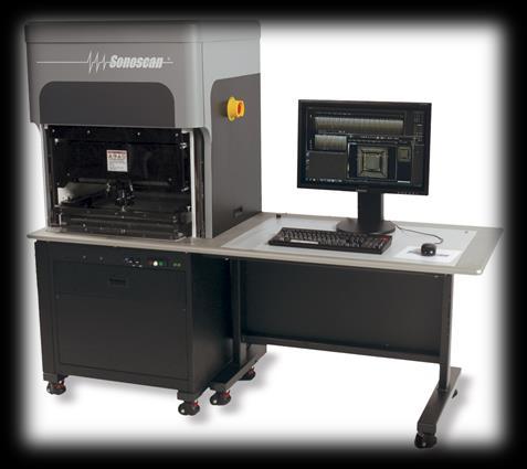
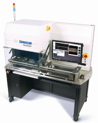
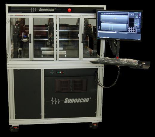

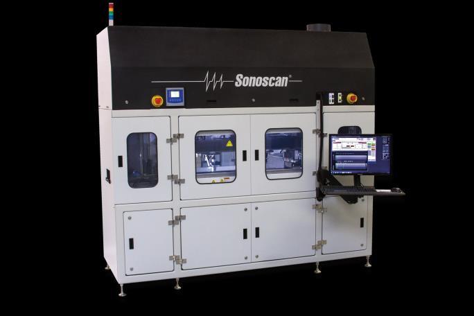
4 From the lab... EQUIPMENT...to the fab.
 Plumbed for water management Class 1000 Cleanroom ready C-Mode Scanning Acoustic")
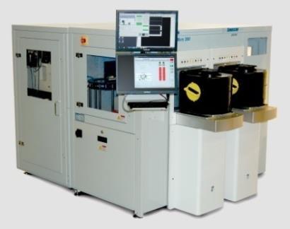
5 C-SAM Gen6 The Latest Generation of C-SAM Technology Sonolytics/Polygate Windows7 (targeting Windows10 in 2017) Plumbed for water management Class 1000 Cleanroom ready C-Mode Scanning Acoustic Microscope
 XYZ Scan")

6 Input Output (A-scan & Image) XYZ Scan Motion Water Tank/Bath Theory of Operation


7 Die face to mold compound interface scan Die face & lead frame to mold compound interface scan Mold compound bulk scan C-scan C-mode Interface Scan Technique


8 Advancements in Transducer Technology ^ Low to High Frequency / 5 to 100 MHz v Very High Frequency / 230, 300 & 400 MHz ^ MHz THRU-Scan TM
9 Beam from Focused Transducer The energy field is an hourglass shaped beam that narrows to the spot size at the waist # Focal length F Diameter Velocity (mm/ s) in Frequency (MHz) mm Depth of Field Spot size Resolution( X) F # 2 Depth of field( Z) 7.1 F # Focal plane
10 Transducers Low Frequency 1. Lower resolution * longer wavelength * larger spot size 2. Longer focal length 3. Greater penetration Very High Frequency 1. Higher resolution * shorter wavelength * smaller spot size 2. Shorter focal length 3. Less penetration Rule of thumb: Ultra/Very High Frequency (230, 300 & 400 MHz) (ex. flip chip bump, bonded wafer, MEMs & stacked die) High Frequency ( MHz) (ex. ubga, TSOP, hybrids, flip chip under fill, bonded wafer and capacitors) ~30 um to ~300 um resolution Low Frequency (10-50 MHz) (ex. BGA, PLCC, PQFP, TSOP and capacitors) ~3 um to ~30 um resolution
11 Resolution Simplified Resolution is the ability to distinguish features that are closely spaced as distinct features. Detectability is the ability to find a feature but not necessarily distinguish them from each other. Lateral resolution is determined by the transducer spot size which is a function of frequency and lens design Axial resolution is determined by the pulse length which is a function of frequency and transducer damping Resolution at high frequencies is deteriorated by sample and coupling fluid absorption


12 180 MHz C-scan Image Voids/disbonds focused and gated within the solder balls C-SCAN 230 MHz C-scan Image Voids/disbonds focused and gated within the solder balls C4 Flip-chip Solder Bump Inspection

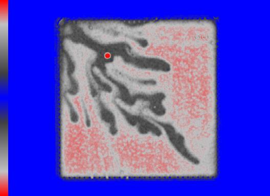
13 Bonded wafer resolution test sample
14 Ultrasound impinges connected interface Ultrasound impinges disconnected interface Glass wafer (Borosilicat glass) 400 µm Trenches with defined width and distances in triplets Silicon wafer 525 µm
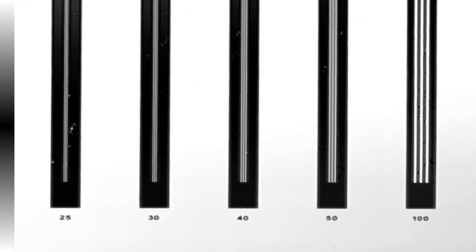
15 Spots / Lines Distance between Lines 3 µm 3 µm 5 µm 5 µm 7 µm 7 µm 10 µm 10 µm 12 µm 12 µm 15 µm 15 µm 17 µm 17 µm 20 µm 20 µm 22 µm 22 µm 25 µm 25 µm 30 µm 30 µm 40 µm 40 µm 50 µm 50 µm 100 µm 100 µm Etched Trenches Bonded area

16 25-100u 15-22u 3-10u

17 Resolution test target showing 3 and 5 micron lines/spacing

18 Enlargement of 3 micron lines/spacing


19 C-SAM Water Fall Transducer ^ Advancements in water management and hardware to aid sample handling and minimize water contact with the sample 19 Water Plume Transducer ^

20 C-SAM Rotational Stage ^ Advancements in water management and hardware to aid sample handling and minimize water contact with the sample 20

21 Advancements in software Virtual Rescanning Module (VRM) VRM allows the entire A-scan to be stored at every pixel position within the image (field of view) A-Scan data from an entire sample is digitally stored in a 3 dimensional data matrix for each X, Y, Z location. Now the part may be rescanned and analyzed off line without needing the part.
22 Virtual Rescan Module (VRM) Virtual Rescanning Module (VRM TM )
 Virtual")
 Horizontal &")
23 Virtual Rescan Module (VRM) Virtual Rescanning Module (VRM TM ) Horizontal & Vertical B-scan
24 Time Domain vs. Frequency Domain Time Domain vs. Frequency Domain Imaging Time Domain Imaging (TDI) is the common and familiar mode in which the brightness or color of each pixel in the image represents the strength (magnitude) and phase (polarity) of an echo in the gate. Frequency Domain Imaging (FDI) is a new analytical mode (FFT) in which the brightness of each pixel represents the strength of a particular frequency component of an echo. FDI can reveal features that are missed with TDI Contrast and resolution can be improved. An echo is a pulse and, therefore, composed of a broad range of frequencies on either side of a peak frequency.
25 Time Domain vs. Frequency Domain Magnitude Frequency Content of a Pulse Frequency (MHz) A pulse may be analyzed to determine the range of frequencies that comprise it.

26 Time Domain vs. Frequency Domain VRM TM Frequency Domain Imaging (FDI)


27 Time Domain vs. Frequency Domain Original Reconstruction 141 MHz 167 MHz 175 MHz 195 MHz 226 MHz VRM TM Frequency Domain Imaging (FDI)
 Multi-focus Multi-gate 1 nanosec")


28 Advancements in software (Polygate Mode) Multi-focus Multi-gate 1 nanosec gating with up to100 gates Polygating provides micro-slicing ( > 1 ns gating) with multiple gates so that numerous interfaces can be collected simultaneously

 with")


 Surface Die Face")
29 Advancements in software Polygating provides micro-slicing ( > 1 ns gating) with multiple gates so that numerous interfaces can be collected simultaneously THRU-Scan (example; BGA) Surface Die Face Die Attach MC/Substrate Interface
.")
30 Integral Mode Each pixel value incorporates the area above and beneath the baseline (not just the largest amplitude). This gives weight to smaller echoes.
31 Acoustic Surface Flatness (ASF) Acoustic Surface Flatness (ASF) The ASF feature is an acoustic profilometer. It is based on the velocity of sound using existing C-Mode Scanning Acoustic Microscope (C-SAM) technology. The ASF feature profiles the sample surface to an accuracy of + 1 micron. A major new option for both product R & D and Failure Analysis labs Compliments current C-SAM capability. For a modest additional cost and no additional floor space the analyst gets the benefits and capability of an additional tool to determine what is wrong with a part.
32 Acoustic Surface Flatness (ASF) JEDEC Standard 95: Design Guide 4.17 BGA Package Measuring and Methodology

33 Acoustic Surface Flatness (ASF) Acoustic Surface Flatness The ASF feature profiles or tracks the position of the front surface echo. It assigns a color in the image based upon the echo s position in time. Echoes that are located farther to the left in the A-Scan are closer to the transducer and will appear white and/or purple in the image. Echoes that are located farther to the right in the A-Scan are further from the transducer and appear orange and/or red in the image.
 Wafer")


34 Acoustic Surface Flatness (ASF) Wafer 2D AMI Image Wafer 3D Contour Wafer 2D ASF Image with 140 μm Warpage Center to Edge
 ASF -")


35 Acoustic Surface Flatness (ASF) ASF - Flip Chip and Substrate Warpage Die only: Acoustic Reflection Die only: Acoustic Flatness Substrate: At least 80 µm of bow Die Substrate Acoustic Flatness
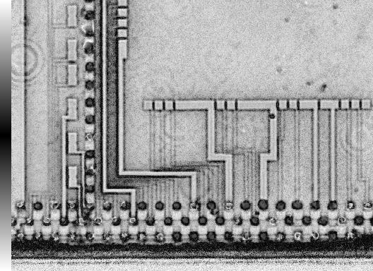
 Q-BAM image")

36 C-scan, Q-BAM & Profile Modes C-scan image (above) Q-BAM image (below) (cross section) Profile Imaging Note: die-tilt in all images
37

38 Sonosimulator - A model of the sample can be built to simulate its acoustic structure with known defects at layers of interest.


39 Sonosimulator - Using a reference waveform a model of the A-scan is generated and compared for each layer of interest.
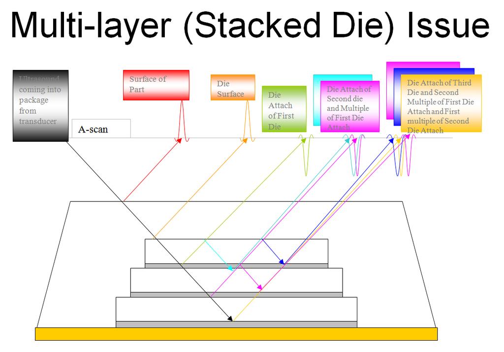
40 Sonosimulator DSA (Die Stack Analysis) Interface Locator Transducer frequency, focus level, and gate positions can then be established, tested and refined prior to transferring the imaging settings. The example shows levels five (5) and six (6) of an eight (8) multi-stack array.


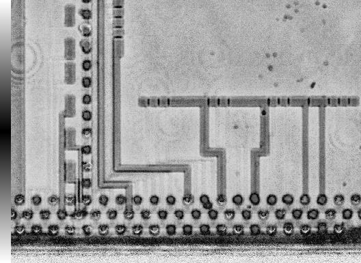
41 Multi-Die Stack Example 4 Stacked Die Adhesive layer between each die Wire bonded Dies 1 to 2 Dies 3 to 4 Dies 2 to 3 41

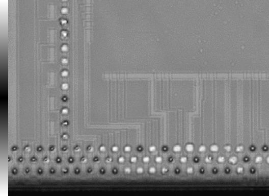
42 3 DIE STACK - 2D C-Scan IMAGE C:\Documents and Settings\lkessler\My Documents\ALS Documents\Presentation Images - 2\Acoustic\BGA- CSP\BGA Stacked Die 1 Multi Die 50.tif

43 3 DIE STACK 3D RECONSTRUCTION
44 CONCLUSION Acoustic Micro Imaging has evolved to meet the needs of the Semiconductor and Microelectronic packaging markets. AMI development will remain to be in the forefront in response to the industry s changing needs. High frequency transducer development and optimization Edge effect reduction for flip chip bump arrays Signal processing and interpretation (new imaging methods) Smart and automated systems Thin layer metrology Frequency Domain Imaging exploration for better analysis. Correlation studies between internal defects and surface warpage Stacked Die analysis program development
Perfecting the Package Bare and Overmolded Stacked Dies. Understanding Ultrasonic Technology for Advanced Package Inspection. A Sonix White Paper
 Perfecting the Package Bare and Overmolded Stacked Dies Understanding Ultrasonic Technology for Advanced Package Inspection A Sonix White Paper Perfecting the Package Bare and Overmolded Stacked Dies Understanding
Wafer Thinning and Thru-Silicon Vias
 Wafer Thinning and Thru-Silicon Vias The Path to Wafer Level Packaging jreche@trusi.com Summary A new dry etching technology Atmospheric Downstream Plasma (ADP) Etch Applications to Packaging Wafer Thinning
INTRODUCTION TO SONOSCAN
 Date: 07/10/2003 INTRODUCTION TO SONOSCAN Dr. Lawrence W. Kessler developed the acoustic microscopy, non-destructive inspection technique at the Zenith Radio Corporation, and in 1973, he acquired patent
Organic light emitting diode (OLED) displays
 displays") Ultra-Short Pulse Lasers Enable Precision Flexible OLED Cutting FLORENT THIBAULT, PRODUCT LINE MANAGER, HATIM HALOUI, APPLICATION MANAGER, JORIS VAN NUNEN, PRODUCT MARKETING MANAGER, INDUSTRIAL PICOSECOND
Ultra-Short Pulse Lasers Enable Precision Flexible OLED Cutting FLORENT THIBAULT, PRODUCT LINE MANAGER, HATIM HALOUI, APPLICATION MANAGER, JORIS VAN NUNEN, PRODUCT MARKETING MANAGER, INDUSTRIAL PICOSECOND
Semiconductors Displays Semiconductor Manufacturing and Inspection Equipment Scientific Instruments
 Semiconductors Displays Semiconductor Manufacturing and Inspection Equipment Scientific Instruments Electronics 110-nm CMOS ASIC HDL4P Series with High-speed I/O Interfaces Hitachi has released the high-performance
Wafer defects can t hide from
 WAFER DEFECTS Article published in Issue 3 2016 Wafer defects can t hide from Park Systems Atomic Force Microscopy (AFM) leader Park Systems has simplified 300mm silicon wafer defect review by automating
NDT Supply.com 7952 Nieman Road Lenexa, KS USA
 ETher ETherCheck Combined Eddy Current & Bond Testing Flaw Detector The ETherCheck is a combined Eddy Current and Bond Testing Flaw Detector which comes with a rich range of features offered by a best
Selection Criteria for X-ray Inspection Systems for BGA and CSP Solder Joint Analysis
 Presented at Nepcon Shanghai 2003 Abstract Selection Criteria for X-ray Inspection Systems for BGA and CSP Solder Joint Analysis Dr. David Bernard, Dage Precision Industries, 158-29 Hua Shan Road, Feng
Abstract. Keywords INTRODUCTION. Electron beam has been increasingly used for defect inspection in IC chip
 Abstract Based on failure analysis data the estimated failure mechanism in capacitor like device structures was simulated on wafer in Front End of Line. In the study the optimal process step for electron
Advanced WLP Platform for High-Performance MEMS. Presented by Dean Spicer, Director of Engineering
 Advanced WLP Platform for High-Performance MEMS Presented by Dean Spicer, Director of Engineering 1 May 11 th, 2016 1 Outline 1. Application Drivers for High Performance MEMS Sensors 2. Approaches to Achieving
Practical Application of the Phased-Array Technology with Paint-Brush Evaluation for Seamless-Tube Testing
 ECNDT 2006 - Th.1.1.4 Practical Application of the Phased-Array Technology with Paint-Brush Evaluation for Seamless-Tube Testing R.H. PAWELLETZ, E. EUFRASIO, Vallourec & Mannesmann do Brazil, Belo Horizonte,
Chapter 6: Real-Time Image Formation
 Chapter 6: Real-Time Image Formation digital transmit beamformer DAC high voltage amplifier keyboard system control beamformer control T/R switch array body display B, M, Doppler image processing digital
Flip Chip Solder Bump Characterization in 3D with X-Ray Microscopy. J. Gelb, A. Gu, L. Hunter, B. Johnson, and W.
 Flip Chip Solder Bump Characterization in 3D with X-Ray Microscopy J. Gelb, A. Gu, L. Hunter, B. Johnson, and W. Yun July 11, 2012 3D X-Ray Microscopy (XRM) Integrated Circuit Sample 3D XRM Data Set 1
X-ray Inspection. Series.
 X-ray Inspection Series www.nordsondage.com 2 Nordson DAGE Quadra X-ray Inspection 3 Nordson DAGE Quadra X-ray Inspection Nordson DAGE Quadra X-ray Inspection 3 Your X-ray Inspection Partner Seeing is
Flexible Electronics Production Deployment on FPD Standards: Plastic Displays & Integrated Circuits. Stanislav Loboda R&D engineer
 Flexible Electronics Production Deployment on FPD Standards: Plastic Displays & Integrated Circuits Stanislav Loboda R&D engineer The world-first small-volume contract manufacturing for plastic TFT-arrays
IN-VISION All rights reserved. IN-VISION GmbH. B2B DLP Light Engine and Optical Solutions
 IN-VISION 2017. All rights reserved. IN-VISION GmbH B2B DLP Light Engine and Optical Solutions Company Long-term experience in development and manufacturing of high-end optical projection lens assemblies
SEMICONDUCTOR TECHNOLOGY -CMOS-
 SEMICONDUCTOR TECHNOLOGY -CMOS- Fire Tom Wada 2011/12/19 1 What is semiconductor and LSIs Huge number of transistors can be integrated in a small Si chip. The size of the chip is roughly the size of nails.
An Overview of the Performance Envelope of Digital Micromirror Device (DMD) Based Projection Display Systems
 Based Projection Display Systems") An Overview of the Performance Envelope of Digital Micromirror Device (DMD) Based Projection Display Systems Dr. Jeffrey B. Sampsell Texas Instruments Digital projection display systems based on the DMD
An Overview of the Performance Envelope of Digital Micromirror Device (DMD) Based Projection Display Systems Dr. Jeffrey B. Sampsell Texas Instruments Digital projection display systems based on the DMD
YXLON Cougar EVO PLUS
 YXLON Cougar EVO PLUS The best small footprint X-ray inspection system for LABORATORY applications Technology with Passion Choose a custom-built EVO solution for premium inspection Why compromise? As technology
Standard Operating Procedure of nanoir2-s
 Standard Operating Procedure of nanoir2-s The Anasys nanoir2 system is the AFM-based nanoscale infrared (IR) spectrometer, which has a patented technique based on photothermal induced resonance (PTIR),
NONDESTRUCTIVE INSPECTION OF A COMPOSITE MATERIAL SAMPLE USING A LASER ULTRASONICS SYSTEM WITH A BEAM HOMOGENIZER
 NONDESTRUCTIVE INSPECTION OF A COMPOSITE MATERIAL SAMPLE USING A LASER ULTRASONICS SYSTEM WITH A BEAM HOMOGENIZER J. M. S. Sakamoto 1, 4, A. Baba 2, B. R. Tittmann 3, J. Mulry 3, M. Kropf, 3 and G. M.
SEMICONDUCTOR TECHNOLOGY -CMOS-
 SEMICONDUCTOR TECHNOLOGY -CMOS- Fire Tom Wada What is semiconductor and LSIs Huge number of transistors can be integrated in a small Si chip. The size of the chip is roughly the size of nails. Currently,
Overcoming Challenges in 3D NAND Volume Manufacturing
 Overcoming Challenges in 3D NAND Volume Manufacturing Thorsten Lill Vice President, Etch Emerging Technologies and Systems Flash Memory Summit 2017, Santa Clara 2017 Lam Research Corp. Flash Memory Summit
High Repetition Rate USP Lasers Improve OLED Cutting Results
 Coherent White Paper May 7, 2018 High Repetition Rate USP Lasers Improve OLED Cutting Results High power ultraviolet, picosecond industrial lasers are widely employed because of their proven ability to
Super Idea for Ultrasonic Inspection
 Super Idea for Ultrasonic Inspection Ultrasound Inspection Ultrasound phased array (PA) and Time Of Flight Diffraction (TOFD), two of the new NDT technologies, have become one important development trend
Applied Materials. 200mm Tools & Process Capabilities For Next Generation MEMS. Dr Michel (Mike) Rosa
 Rosa") Applied Materials 200mm Tools & Process Capabilities For Next Generation MEMS Dr Michel (Mike) Rosa 200mm MEMS Global Product / Marketing Manager, Components and Systems Group (CSG), Applied Global Services
Applied Materials 200mm Tools & Process Capabilities For Next Generation MEMS Dr Michel (Mike) Rosa 200mm MEMS Global Product / Marketing Manager, Components and Systems Group (CSG), Applied Global Services
Minimize your cost for Phased Array & TOFD
 Minimize your cost for Phased Array & TOFD Latest ultrasonic flaw detector from SIUI, incorporates the latest advancements in Encoder In/Out UT/ TOFD Probe high-performance Phased Array and TOFD detection
Digital Light Processing
 A Seminar report On Digital Light Processing Submitted in partial fulfillment of the requirement for the award of degree of Bachelor of Technology in Computer Science SUBMITTED TO: www.studymafia.org SUBMITTED
An Alternative Architecture for High Performance Display R. W. Corrigan, B. R. Lang, D.A. LeHoty, P.A. Alioshin Silicon Light Machines, Sunnyvale, CA
 R. W. Corrigan, B. R. Lang, D.A. LeHoty, P.A. Alioshin Silicon Light Machines, Sunnyvale, CA Abstract The Grating Light Valve (GLV ) technology is being used in an innovative system architecture to create
Large-Scale Polysilicon Surface Micro-Machined Spatial Light Modulator
 Large-Scale Polysilicon Surface Micro-Machined Spatial Light Modulator Clara Dimas, Julie Perreault, Steven Cornelissen, Harold Dyson, Peter Krulevitch, Paul Bierden, Thomas Bifano, Boston Micromachines
Advanced Sensor Technologies
 Advanced Sensor Technologies Jörg Amelung Fraunhofer Institute for Photonics Microsystems Name of presenter date Sensors as core element for IoT Next phase of market grow New/Advanced Requirements based
21 rue La Noue Bras de Fer Nantes - France Phone : +33 (0) website :
 website :") 21 rue La Noue Bras de Fer - 44200 Nantes - France Phone : +33 (0) 240 180 916 - email : info@systemplus.fr - website : www.systemplus.fr 2012 September - Version 1 Written by: Maher Sahmimi DISCLAIMER
21 rue La Noue Bras de Fer - 44200 Nantes - France Phone : +33 (0) 240 180 916 - email : info@systemplus.fr - website : www.systemplus.fr 2012 September - Version 1 Written by: Maher Sahmimi DISCLAIMER
PRACTICAL APPLICATION OF THE PHASED-ARRAY TECHNOLOGY WITH PAINT-BRUSH EVALUATION FOR SEAMLESS-TUBE TESTING
 PRACTICAL APPLICATION OF THE PHASED-ARRAY TECHNOLOGY WITH PAINT-BRUSH EVALUATION FOR SEAMLESS-TUBE TESTING R.H. Pawelletz, E. Eufrasio, Vallourec & Mannesmann do Brazil, Belo Horizonte, Brazil; B. M. Bisiaux,
Cover Sheet. Scanning Report of Flexible Riser Pipe Section EVI /7/2005. Inspection Report
 Cover Sheet Document Number EVI-2005-0002 Document Date 7/7/2005 Document Title Customer -other- AEA Technologies Type Inspection Report Prepared by: Date: Reviewed by: Date: Approved by: Date: Evisive,
MOST - Roadmap Physical Layer & Connectivity from 150Mbps to 5Gbps
 MOST - Roadmap Physical Layer & Connectivity from 150Mbps to 5Gbps 13th MOST(R) Interconnectivity Conference Asia on November 15, 2012 in Seoul, South Korea Andreas Engel Manager Advanced Infotainment
Dynamic IR Scene Projector Based Upon the Digital Micromirror Device
 Dynamic IR Scene Projector Based Upon the Digital Micromirror Device D. Brett Beasley, Matt Bender, Jay Crosby, Tim Messer, and Daniel A. Saylor Optical Sciences Corporation www.opticalsciences.com P.O.
Nano-Imprint Lithography Infrastructure: Imprint Templates
 Nano-Imprint Lithography Infrastructure: Imprint Templates John Maltabes Photronics, Inc Austin, TX 1 Questions to keep in mind Imprint template manufacturability Resolution Can you get sub30nm images?
Characterization and improvement of unpatterned wafer defect review on SEMs
 Characterization and improvement of unpatterned wafer defect review on SEMs Alan S. Parkes *, Zane Marek ** JEOL USA, Inc. 11 Dearborn Road, Peabody, MA 01960 ABSTRACT Defect Scatter Analysis (DSA) provides
Layout Analysis Analog Block
 Layout Analysis Analog Block Sample Report Analysis from an HD Video/Audio SoC For any additional technical needs concerning semiconductor and electronics technology, please call Sales at Chipworks. 3685
EECS150 - Digital Design Lecture 2 - CMOS
 EECS150 - Digital Design Lecture 2 - CMOS January 23, 2003 John Wawrzynek Spring 2003 EECS150 - Lec02-CMOS Page 1 Outline Overview of Physical Implementations CMOS devices Announcements/Break CMOS transistor
Leveraging 300 mm Technology Solutions to Enable New MEMS Process Capabilities
 Leveraging 300 mm Technology Solutions to Enable New MEMS Process Capabilities Evan Patton Semicon Europa November 2017 Lam Research Corp. 1 Presentation Outline The Internet of Things (IoT) as a market
High ResolutionCross Strip Anodes for Photon Counting detectors
 High ResolutionCross Strip Anodes for Photon Counting detectors Oswald H.W. Siegmund, Anton S. Tremsin, Robert Abiad, J. Hull and John V. Vallerga Space Sciences Laboratory University of California Berkeley,
Power Device Analysis in Design Flow for Smart Power Technologies
 Power Device Analysis in Design Flow for Smart Power Technologies A.Bogani, P.Cacciagrano, G.Ferre`, L.Paciaroni, M.Verga ST Microelectronics, via Tolomeo 1 Cornaredo 20010, Milano, Italy M.Ershov,Y.Feinberg
Alien Technology Corporation White Paper. Fluidic Self Assembly. October 1999
 Alien Technology Corporation White Paper Fluidic Self Assembly October 1999 Alien Technology Corp Page 1 Why FSA? Alien Technology Corp. was formed to commercialize a proprietary technology process, protected
Advanced Display Manufacturing Technology
 Advanced Display Manufacturing Technology John Busch Vice President, New Business Development Display and Flexible Technology Group September 28, 2017 Safe Harbor This presentation contains forward-looking
Impact of DMD-SLMs errors on reconstructed Fourier holograms quality
 Journal of Physics: Conference Series PAPER OPEN ACCESS Impact of DMD-SLMs errors on reconstructed Fourier holograms quality To cite this article: D Yu Molodtsov et al 2016 J. Phys.: Conf. Ser. 737 012074
ABSTRACT. Keywords: 3D NAND, FLASH memory, Channel hole, Yield enhancement, Defect inspection, Defect reduction DISCUSSION
 Yield enhancement of 3D flash devices through broadband brightfield inspection of the channel hole process module Jung-Youl Lee a, Il-Seok Seo a, Seong-Min Ma a, Hyeon-Soo Kim a, Jin-Woong Kim a DoOh Kim
Through Silicon Via Testing Known Good Die (KGD) or Probably Good Die (PGD) Doug Lefever Advantest
 or Probably Good Die (PGD) Doug Lefever Advantest") Through Silicon Via Testing Known Good Die (KGD) or Probably Good Die (PGD) Doug Lefever Advantest Single Die Fab Yield will drive Cost Equation. Yield of the device to be stacked 100% 90% 80% Yield of
Through Silicon Via Testing Known Good Die (KGD) or Probably Good Die (PGD) Doug Lefever Advantest Single Die Fab Yield will drive Cost Equation. Yield of the device to be stacked 100% 90% 80% Yield of
Challenges in the design of a RGB LED display for indoor applications
 Synthetic Metals 122 (2001) 215±219 Challenges in the design of a RGB LED display for indoor applications Francis Nguyen * Osram Opto Semiconductors, In neon Technologies Corporation, 19000, Homestead
EE C247B ME C218 Introduction to MEMS Design Spring 2017
 EE C247B ME C218 Introduction to MEMS Design Spring 2017 Prof. Clark T.-C. Nguyen Dept. of Electrical Engineering & Computer Sciences University of California at Berkeley Berkeley, CA 94720 Lecture Module
Durham Magneto Optics Ltd. NanoMOKE 3 Wafer Mapper. Specifications
 Durham Magneto Optics Ltd NanoMOKE 3 Wafer Mapper Specifications Overview The NanoMOKE 3 Wafer Mapper is an ultrahigh sensitivity Kerr effect magnetometer specially configured for measuring magnetic hysteresis
Polygon Scanners Capabilities, Applications and System integration. considerations
 Workshop ALPS Swissphotonics - APPOLO Polygon Scanners Capabilities, Applications and System integration considerations Lars Penning CEO Next Scan Technology Innovating and leading polygon scanner technology
Explore the Art of Detection
 Y.Cougar Microfocus and nanofocus X-ray inspection systems for the electronics industries Explore the Art of Detection Technology with Passion Our specialty: The Art of Detection. Developing outstanding
Verification of HBM through Direct Probing on MicroBumps
 Verification of HBM through Direct Probing on MicroBumps FormFactor Sung Wook Moon SK hynix Outline HBM market HBM test flow Device structure overview Key test challenges addressed Signal delivery and
Characterizing Transverse Beam Dynamics at the APS Storage Ring Using a Dual-Sweep Streak Camera
 Characterizing Transverse Beam Dynamics at the APS Storage Ring Using a Dual-Sweep Streak Camera Bingxin Yang, Alex H. Lumpkin, Katherine Harkay, Louis Emery, Michael Borland, and Frank Lenkszus Advanced
Future trends for SiP In Medical Implant Applications
 Future trends for SiP In Medical Implant Applications Piers Tremlett, Zarlink Semiconductor NMI at TWI, 12 Dec 07 A case study This presentation uses Zarlink s Medical RF device To consider potential embedded
NDT Applications of All-Electronic 3D Terahertz Imaging
 Introduction NDT Applications of All-Electronic 3D Terahertz Imaging Stefan BECKER *, Andreas Keil *, Heinrich Nolting * * Becker Photonik GmbH, D-32457 Porta Westfalica, Germany! Basics of All-Electronic
Lecture 17: Introduction to Design For Testability (DFT) & Manufacturing Test
 & Manufacturing Test") Lecture 17: Introduction to Design For Testability (DFT) & Manufacturing Test Mark McDermott Electrical and Computer Engineering The University of Texas at Austin Agenda Introduction to testing Logical
Lecture 17: Introduction to Design For Testability (DFT) & Manufacturing Test Mark McDermott Electrical and Computer Engineering The University of Texas at Austin Agenda Introduction to testing Logical
ONE SENSOR MICROPHONE ARRAY APPLICATION IN SOURCE LOCALIZATION. Hsin-Chu, Taiwan
 ICSV14 Cairns Australia 9-12 July, 2007 ONE SENSOR MICROPHONE ARRAY APPLICATION IN SOURCE LOCALIZATION Percy F. Wang 1 and Mingsian R. Bai 2 1 Southern Research Institute/University of Alabama at Birmingham
UNIT IV CMOS TESTING. EC2354_Unit IV 1
 UNIT IV CMOS TESTING EC2354_Unit IV 1 Outline Testing Logic Verification Silicon Debug Manufacturing Test Fault Models Observability and Controllability Design for Test Scan BIST Boundary Scan EC2354_Unit
Timing EECS141 EE141. EE141-Fall 2011 Digital Integrated Circuits. Pipelining. Administrative Stuff. Last Lecture. Latch-Based Clocking.
 EE141-Fall 2011 Digital Integrated Circuits Lecture 2 Clock, I/O Timing 1 4 Administrative Stuff Pipelining Project Phase 4 due on Monday, Nov. 21, 10am Homework 9 Due Thursday, December 1 Visit to Intel
Illumination Challenges in Non- Industrial Vision Applications. Simon Stanley Managing Director ProPhotonix IRL Ltd
 Illumination Challenges in Non- Industrial Vision Applications Simon Stanley Managing Director ProPhotonix IRL Ltd ProPhotonix designs and manufactures high-quality LED systems and laser modules for the
In-process inspection: Inspector technology and concept
 Inspector In-process inspection: Inspector technology and concept Need to inspect a part during production or the final result? The Inspector system provides a quick and efficient method to interface a
Design and Implementation of an AHB VGA Peripheral
 Design and Implementation of an AHB VGA Peripheral 1 Module Overview Learn about VGA interface; Design and implement an AHB VGA peripheral; Program the peripheral using assembly; Lab Demonstration. System
Results on 0.7% X0 thick Pixel Modules for the ATLAS Detector.
 Results on 0.7% X0 thick Pixel Modules for the ATLAS Detector. INFN Genova: R.Beccherle, G.Darbo, G.Gagliardi, C.Gemme, P.Netchaeva, P.Oppizzi, L.Rossi, E.Ruscino, F.Vernocchi Lawrence Berkeley National
Compact Muon Solenoid Detector (CMS) & The Token Bit Manager (TBM) Alex Armstrong & Wyatt Behn Mentor: Dr. Andrew Ivanov
 & The Token Bit Manager (TBM) Alex Armstrong & Wyatt Behn Mentor: Dr. Andrew Ivanov") Compact Muon Solenoid Detector (CMS) & The Token Bit Manager (TBM) Alex Armstrong & Wyatt Behn Mentor: Dr. Andrew Ivanov Part 1: The TBM and CMS Understanding how the LHC and the CMS detector work as a
Compact Muon Solenoid Detector (CMS) & The Token Bit Manager (TBM) Alex Armstrong & Wyatt Behn Mentor: Dr. Andrew Ivanov Part 1: The TBM and CMS Understanding how the LHC and the CMS detector work as a
RPV and Primary Circuit Inspection. Pressure Vessel Inspection Codes for phased Arrays M. Moles, Olympus NDT, Canada
 RPV and Primary Circuit Inspection Pressure Vessel Inspection Codes for phased Arrays M. Moles, Olympus NDT, Canada ABSTRACT Pressure vessel and piping welds require inspection to code worldwide to minimize
ABRS Series. Air-Bearing Rotary Stage. Direct-drive, slotless brushless servomotor. Zero cogging motor for outstanding velocity stability
 ABRS Series Air-Bearing Rotary Stage Direct-drive, slotless brushless servomotor Zero cogging motor for outstanding velocity stability Outstanding error motion and wobble performance Direct coupled, high
LEP400 Etch Depth Monitor Real-time, in-situ plasma etch depth monitoring and end point control plus co-linear wafer vision system
 LEP400 Etch Depth Monitor Real-time, in-situ plasma etch depth monitoring and end point control plus co-linear wafer vision system Base Configuration Etch Depth Monitoring LEP400 Recessed Window Plasma
MEMS Mirror: A8L AU-TINY48.4
 MEMS Mirror: A8L2.2-4600AU-TINY48.4 Description: The new A8L2 actuator is based on an established robust two-axis MEMS design which supports various bonded mirror sizes in largeangle beam steering. Previous
FDTD_SPICE Analysis of EMI and SSO of LSI ICs Using a Full Chip Macro Model
 FDTD_SPICE Analysis of EMI and SSO of LSI ICs Using a Full Chip Macro Model Norio Matsui Applied Simulation Technology 2025 Gateway Place #318 San Jose, CA USA 95110 matsui@apsimtech.com Neven Orhanovic
Application Note AN SupIRBuck MCM Power Quad Flat No-lead (PQFN) Inspection Application Note
 Inspection Application Note") Application Note AN-1133 SupIRBuck MCM Power Quad Flat No-lead (PQFN) Inspection Application Note Table of Contents Page Inspection techniques... 3 Examples of good assembly... 3 Summary of rejection criteria...
Application Note AN-1133 SupIRBuck MCM Power Quad Flat No-lead (PQFN) Inspection Application Note Table of Contents Page Inspection techniques... 3 Examples of good assembly... 3 Summary of rejection criteria...
DEPFET Active Pixel Sensors for the ILC
 DEPFET Active Pixel Sensors for the ILC Laci Andricek for the DEPFET Collaboration (www.depfet.org) The DEPFET ILC VTX Project steering chips Switcher thinning technology Simulation sensor development
Lab 6: Edge Detection in Image and Video
 http://www.comm.utoronto.ca/~dkundur/course/real-time-digital-signal-processing/ Page 1 of 1 Lab 6: Edge Detection in Image and Video Professor Deepa Kundur Objectives of this Lab This lab introduces students
DESIGNING MEMS MICROPHONES FROM CONCEPT TO FINISHED GDSII IN ABOUT TWO WEEKS
 DESIGNING MEMS MICROPHONES FROM CONCEPT TO FINISHED GDSII IN ABOUT TWO WEEKS A M S D E S I G N & V E R I F I C A T I O N C A S E S T U D Y w w w. m e n t o r. c o m ABOUT THE MEMS MICROPHONE MARKET Knowles
Reading a GEM with a VLSI pixel ASIC used as a direct charge collecting anode. R.Bellazzini - INFN Pisa. Vienna February
 Reading a GEM with a VLSI pixel ASIC used as a direct charge collecting anode Ronaldo Bellazzini INFN Pisa Vienna February 16-21 2004 The GEM amplifier The most interesting feature of the Gas Electron
Screen investigations for low energetic electron beams at PITZ
 1 Screen investigations for low energetic electron beams at PITZ S. Rimjaem, J. Bähr, H.J. Grabosch, M. Groß Contents Review of PITZ setup Screens and beam profile monitors at PITZ Test results Summary
AltiumLive 2017: Effective Methods for Advanced Routing
 AltiumLive 2017: Effective Methods for Advanced Routing Charles Pfeil Senior Product Manager Dave Cousineau Sr. Field Applications Engineer Charles Pfeil Senior Product Manager Over 50 years of experience
Transforming Electronic Interconnect Breaking through historical boundaries Tim Olson Founder & CTO
 Transforming Electronic Interconnect Breaking through historical boundaries Tim Olson Founder & CTO Remember when? There were three distinct industries Wafer Foundries SATS EMS Semiconductor Devices Nanometers
Spatial Light Modulators XY Series
 Spatial Light Modulators XY Series Phase and Amplitude 512x512 and 256x256 A spatial light modulator (SLM) is an electrically programmable device that modulates light according to a fixed spatial (pixel)
MEMS Technologies Dresden - Product Development and Fabrication at IPMS Dresden
 MEMS Technologies Dresden - Product Development and Fabrication at IPMS Dresden MEMS Technologies Dresden - Product Development and Fabrication at IPMS Dresden Michael Müller, Matthias List Outline FhG-IPMS
COPYRIGHTED MATERIAL. Introduction. 1.1 Overview of Projection Displays
 1 Introduction 1.1 Overview of Projection Displays An electronic display is a device or system which converts electronic signal information representing video, graphics and/or text to a viewable image
HOT LINKS Trade Show Schedule ISO Certification Contact
 July 2012 HOT LINKS Trade Show Schedule ISO Certification Contact Single-Field Scanning - Reduced Sensitivity To Contamination, Higher Quality PRODUCT SPOTLIGHT The type of scanning in harsh operating
DIRECT DRIVE ROTARY TABLES SRT SERIES
 DIRECT DRIVE ROTARY TABLES SRT SERIES Key features: Direct drive Large center aperture Brushless motor design Precision bearing system Integrated position feedback Built-in thermal sensors ServoRing rotary
WI, USA; 3 QinetiQ Ltd, Farnborough, Hampshire, UK
 RAPID, LOW-COST, FULL-WAVEFORM MAPPING AND ANALYSIS WITH ULTRASONIC ARRAYS D. Lines 1, J. Skramstad 2, and R. Smith 3 1 Diagnostic Sonar Ltd, Livingston, West Lothian, UK; 2 NDT Solutions Inc, New Richmond,
Television History. Date / Place E. Nemer - 1
 Television History Television to see from a distance Earlier Selenium photosensitive cells were used for converting light from pictures into electrical signals Real breakthrough invention of CRT AT&T Bell
Pressure sensor. Surface Micromachining. Residual stress gradients. Class of clean rooms. Clean Room. Surface micromachining
 Pressure sensor Surface Micromachining Deposit sacrificial layer Si PSG By HF Poly by XeF2 Pattern anchors Deposit/pattern structural layer Etch sacrificial layer Surface micromachining Structure sacrificial
Imaging of Impacted Composite Armours using Data Clustering
 18 th World Conference on Nondestructive Testing, 16-20 April 2012, Durban, South Africa Imaging of Impacted Composite Armours using Data Clustering Sutanu SAMANTA 1 and Debasis DATTA 2 1 Department of
MEMS METROLOGY USING A STROBED INTERFEROMETRIC SYSTEM
 XVII IMEKO World Congress Metrology in the 3rd Millennium June 22 27, 2003, Dubrovnik, Croatia MEMS METROLOGY USING A STROBED INTERFEROMETRIC SYSTEM Erik Novak, Der-Shen Wan, Paul Unruh, Michael Schurig
UV Nanoimprint Tool and Process Technology. S.V. Sreenivasan December 13 th, 2007
 UV Nanoimprint Tool and Process Technology S.V. Sreenivasan December 13 th, 2007 Agenda Introduction Need tool and process technology that can address: Patterning and CD control Alignment and Overlay Defect
ABSTRACT 1 INTRODUCTION
 Novel lithography technique using an ASML Stepper/Scanner for the manufacture of display devices in MEMS world ASML US, Inc Special Applications, 6580 Via Del Oro San Jose, CA 95119 Keith Best, Pankaj
MagnaChip HV7161SP 1.3 Megapixel CMOS Image Sensor Process Review
 September 21, 2005 MagnaChip HV7161SP 1.3 Megapixel Process Review For questions, comments, or more information about this report, or for any additional technical needs concerning semiconductor technology,
Innovative Fast Timing Design
 Innovative Fast Timing Design Solution through Simultaneous Processing of Logic Synthesis and Placement A new design methodology is now available that offers the advantages of enhanced logical design efficiency
8 DIGITAL SIGNAL PROCESSOR IN OPTICAL TOMOGRAPHY SYSTEM
 Recent Development in Instrumentation System 99 8 DIGITAL SIGNAL PROCESSOR IN OPTICAL TOMOGRAPHY SYSTEM Siti Zarina Mohd Muji Ruzairi Abdul Rahim Chiam Kok Thiam 8.1 INTRODUCTION Optical tomography involves
De-embedding Techniques For Passive Components Implemented on a 0.25 µm Digital CMOS Process
 PIERS ONLINE, VOL. 3, NO. 2, 27 184 De-embedding Techniques For Passive Components Implemented on a.25 µm Digital CMOS Process Marc D. Rosales, Honee Lyn Tan, Louis P. Alarcon, and Delfin Jay Sabido IX
Focused Ion Beam System MI4050
 SCIENTIFIC INSTRUMENT NEWS 2016 Vol. 7 SEPTEMBER Technical magazine of Electron Microscope and Analytical Instruments. Technical Explanation Focused Ion Beam System MI4050 Yasushi Kuroda *1, Yoshihisa
PRODUCT GUIDE CEL5500 LIGHT ENGINE. World Leader in DLP Light Exploration. A TyRex Technology Family Company
 A TyRex Technology Family Company CEL5500 LIGHT ENGINE PRODUCT GUIDE World Leader in DLP Light Exploration Digital Light Innovations (512) 617-4700 dlinnovations.com CEL5500 Light Engine The CEL5500 Compact
The future of microled displays using nextgeneration
 The future of microled displays using nextgeneration technologies Introduction MicroLEDs (micro-light-emitting diodes) are an emerging display technology that, as the name implies, use very small LEDs
Scan. This is a sample of the first 15 pages of the Scan chapter.
 Scan This is a sample of the first 15 pages of the Scan chapter. Note: The book is NOT Pinted in color. Objectives: This section provides: An overview of Scan An introduction to Test Sequences and Test
The hybrid photon detectors for the LHCb-RICH counters
 7 th International Conference on Advanced Technology and Particle Physics The hybrid photon detectors for the LHCb-RICH counters Maria Girone, CERN and Imperial College on behalf of the LHCb-RICH group