Practical De-embedding for Gigabit fixture. Ben Chia Senior Signal Integrity Consultant 5/17/2011
|
|
|
- Cameron Black
- 5 years ago
- Views:
Transcription

1 Practical De-embedding for Gigabit fixture Ben Chia Senior Signal Integrity Consultant 5/17/2011
2 Topics Why De-Embedding/Embedding? De-embedding in Time Domain De-embedding in Frequency Domain De-embedding example Compliance test examples Accuracy consideration 2
3 Terminalolgy De-Embedding Remove fixture effect from the measurement Example: remove probes, SMA+traces Embedding Add a cable to see what happen to the signal Example: test receiver sensitivity by adding a 4-inch cable between the driver and DUT 3
4 De-embedding Example 4
5 Measurement Reference Plane 5

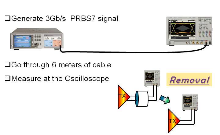
6 6-meter cable de-embedding Does your scope show the real waveform? ` 6

7 Example: De-embedding Probes 7

8 More Example: DDR2 Device Fixture DDR2 How to remove this fixture effect? 8

9 DDR2 Fixture De-Embedding Scope performs de-embedding 9
10 De-Embedding Calibration Both VNA/TDR have firmware to simplify de-embedding process Probe de-embedding Fixture de-embedding 10
11 TDR De-embedding Example Calibrate with SMA standard Short Load Connect Port 1 to SMA to measure S11 PCB trace SMA How to capture S11 at the package ball? 11
12 TDR De-embedding Example Agilent 54754A Option A Step 1: Capture fixture S4P ( Pad+trace +SMA ) Calibrate using SMA standard and Probe standard Measure DUT Port1: Pad Probing Port2: Probing SMA Capture S4P of SMA+Trace in Time Domain 12
13 Probing Example 13

14 TDR De-embedding Option A Step 1: Capture fixture S4P for trace with SMA at one end and PCB pads at the other end? Step 2: De-embedding fixture trace using ADS 14

15 TDR De-embedding Option B De-embedding including SMA using on-board calibration short and load standard short Measurement 50 ohm load DUT 15

16 Return Loss De-embedding 16
17 De-Embedding using VNA Equipment : Agilent ENA Calibration : SOLT DUT: Port 1, 2 - SMA Port 3, 4 - USB connectors Require TRL-like PCB calibration standard Fixture delay estimation use port extension to measure fixture delay Port1,2 SMA USB Port3,4 17

18 USB3.0 De-embedding Example A C How to measure S4P from A to C? 18

19 USB3.0 De-embedding Example A C How to measure S4P from A to C? 19


20 De-embedding fixture and Calibration board C A De-embedding fixture Calibration Board 20
21 Calibration Fixture Calibration Standard Open/Short/Load Port1, 3 use coaxial standard Port 2,4 use calibration board Delay/through Port 1-2 use coaxial standard Port 3-4 use 2x fixture trace Prot 1-3, 2-4, 1-4, 2-3 use 1x fixture trace 1x fixture trace Open/Short/load 1x thru trace 2x thru trace 21
22 Example : Return Loss Measurement Introduction Return loss measurement When return loss is not passing Return loss fixture removal How to fix the return loss problem Summary 22

23 Sata Interconnect Return Loss Specification limits the reflected energy 23
24 Return Loss Definition Return Loss = 20log 10 Z Z o o Z Z L L or 20log 10 V V i r where Zo is the Tx/Rx differential output/input impedance Z L is the link differential impedance Vi is the differential voltage incident upon Rx/Tx Vr is the differential reflected voltage from Tx/Rx Slid

25 Common Mode vs. Differential Mode Slid
26 Return Loss Measurement Many design can not meet return loss requirement Return loss accuracy and repeatability become crutial Both TDR ( time domain ) and VNA (frequency domain) can be used for return loss measurement Recommend VNA for marginal design Accuracy noise floor and calibration Repeatability - calibration standard 26

27 Return Loss Element Termination and IO circuit Ask circuit designer to reduce mismatch in both differential mode and common mode Differential driver circuit state Design special circuit to set IO to static 1 or 0 state Capable to set static de-emphasis state Pattern Blocking Capacitor 27
28 Blocking Caps The 100nF off chip coupling capacitor leads to a coupling time constant of 10 us. Such a long time constant is needed to limit baseline wander with scrambled data Make sure DC blocking capacitor is in placed for active transmitter return loss measurement - TDR/VNA port may gradually get damaged 28
29 How to Pass Return Loss Small IO capacitance less reflection Uniform impedance less reflection Shorter and uniform impedance fixture May not require fixture de-embedding if margin is large enough Long fixture trace and via will have better return loss number because reflection are attenuated by the long trace You got wrong result 29
30 Vector Network Analyzer Frequency Domain Equipment Single ended measurement Convert to differential mode and common mode with software 30
31 How Return Loss Are Measured today VNA Setup 0 dbm (1mw) Tx Setup One driver on AC high state ( < Voh) Another driver on AC low state (> Vol) Rx Setup Activate terminator 31
32 Return Loss De-embedding Simulation to remove the SMA, PCB trace, via and fingers. The return loss after de-embedding are usually worse than the VNA data measured at the SMA or PCB fingers 32

33 SMA Anti-pad Optimization Antipad diameter under trace Antipad diameter above trace Signal via radius Trace moved to different layer Ground via distance SMA Optimized Anti-pad Design Optimization critera ohm -- low return loss 33

34 Return Loss Tuning Strategy : Simulation Pkg Stub Pkg Via Pkg Trace Bond Wire Ri Ci Rterm Agilent ADS or any spice tool can make this simple model 34
35 Transmit Port B Return Loss Including PCB Red: Model Blue: Measured An Example: XAUI
36 Receive Port B Return Loss Including PCB Red: Model Blue: Measured 36
37 Transmit Port B Return Loss Not Including Socket
38 Receive Port B Return Loss Not Including Socket 38
39 Pink: Measured Rx Black: Model Rx Violations at 3Ghz Slide What was wrong in this design?
40 Circuit for Return Loss Calculation CL: Cell Capacitance RS: Cell Series Resistance RL: Termination resistance Z0: Reference Resistance for S11 Calculation Z0 S11 RL CL RS 40
41 Rx Return loss model vs measured SMA Pcb via Package Pad/ball/via Ci 83ps Slide
42 Rx Return Loss Debugging Identify the elements from S11 plot 3GHz = 333ps Reflection at 180 degree 165ps Round trip delay 83ps Delay from PCB pad to Pakage pad ~83ps Fix: Increase the impedance to 50 ohm at the PCB via and package via in the model Slide
43 Pink: measured Rx Black: modified Rx model Replace PCB via and Package pads to 50 ohm Slide
44 TX : Increase PCB and Pads to 50 ohm Slide
45 Return Loss Summary Measurement based return loss provides accurate results after de-embedding SMA and lead-in traces on the text fixture SMA Impedance discontinuity can affect return loss significantly Optimized SMA anti-pad design can improve return loss accuracy Return loss measurement can be verified by careful modeling the package and PCB interconnect transistion 45
46 Hands-on Lab USB Compliance test Configuration Different fixture design comparison Insertion loss Eye diagram Conclusions 46
47 USB 3.0 Tx Compliance Channels Compliance Channels are defined to test Transmitter for worst case conditions. Device Tx TP1 Host Tx TP0 Worst Case Channel for Hosts 5 Device PCB Trace 3M Cable Host Tx TP1 3 Meter USB 3.0 Cable Worst Case Channel for Devices 11 Device PCB Trace 3M Cable Device Tx TP0 47


48 GRL Case Study: Three USB 3.0 Probing Setups for Device Testing TP0 USB-IF Fixture with 4 USB3.0 Cable INTEL_TIER2.S4P Agilent Fixture with 4 USB3.0 Cable TP0 AGILENT_TIER2.S4P Scope Measurement Plane TP0 LITEK_TIER2.S4P LiTek Fixture with 0 Cable TP0 (Device Connector) FixtureX.S4P Measurement Plane 48


49 Embed of USB 3.0 Cable + Host Channel Compliance Test Point 100mV Eye Mask CTLE In Scope SW TP1 Transmit Channel TP0 cascade_cable_back.s4p 49
50 Differential Insertion Loss Comparison 2.5GHz Nyquist Frequency 50


51 Results LiTek + 0 Cable Agilent + 4 Cable Intel + 4 Scope TP0 DUT TP1-Eq Compliance Point 250mV 234mV 228mV 51
52 Conclusions LiTek with 0 cable provides 6-9% Higher Voltage Margin than 4 Cable based fixtures. Intel Fixture, which is recommended by the USB-IF provides the least amount of margin and represents the worst case of the three fixtures tested. 52
53 Thank You 53
54 Backup - VNA SOLT Reference Plane 54

55 Transmit-Reflect-Line Calibration TRL Calibration SOLT Calibration Calibration standard designed on the same PCB as the device under test 55
56 How to Improve TRL Calibration Reduce connector reflection Increase trace width to reduce excessive solder variation Ensure soldering has minimum variation PCB trace Use wider trace to reduce impedance variation Use better material to reduce variation in impedance and delay Layout trace 45 degree with woven glass Specify denser woven glass for FR4 material 56
57 New: Two Tier Adaptor Removal Calibration MicroProbe Tips 57

58 Probing Example of TRL kit 58
Optimizing BNC PCB Footprint Designs for Digital Video Equipment
 Optimizing BNC PCB Footprint Designs for Digital Video Equipment By Tsun-kit Chin Applications Engineer, Member of Technical Staff National Semiconductor Corp. Introduction An increasing number of video
A Simple, Yet Powerful Method to Characterize Differential Interconnects
 A Simple, Yet Powerful Method to Characterize Differential Interconnects Overview Measurements in perspective The automatic fixture removal (AFR) technique for symmetric fixtures Automatic Fixture Removal
Emphasis, Equalization & Embedding
 Emphasis, Equalization & Embedding Cleaning the Rusty Channel Gustaaf Sutorius Application Engineer Agilent Technologies gustaaf_sutorius@agilent.com Dr. Thomas Kirchner Senior Application Engineer Digital
30 GHz Attenuator Performance and De-Embedment
 30GHz De-Embedment Application Note - Page 1 of 6 Theory of De-Embedment. Due to the need for smaller packages and higher signal integrity a vast majority of todays RF and Microwave components are utilizing
Senior Project Manager / AEO
 Kenny Liao 2018.12.18&20 Senior Project Manager / AEO Measurement Demo Prepare instrument for measurement Calibration Fixture removal Conclusion What next? Future trends Resources Acquire channel data
RF Characterization Report
 CJT Series Circular RF Twinax Jack CJT-T-P-HH-ST-TH1 CJT-T-P-HH-RA-BH1 Mated With C28S-XX.XX-SPS8-SPS8 Description: Fully Mated Circular RF Shielded Twisted Pair Twinax Cable Assembly Samtec Inc. WWW.SAMTEC.COM
De-embedding Gigaprobes Using Time Domain Gating with the LeCroy SPARQ
 De-embedding Gigaprobes Using Time Domain Gating with the LeCroy SPARQ Dr. Alan Blankman, Product Manager Summary Differential S-parameters can be measured using the Gigaprobe DVT30-1mm differential TDR
HMC958LC5 HIGH SPEED LOGIC - SMT. Typical Applications. Features. Functional Diagram. General Description
 Typical Applications Features The HMC958LC5 is ideal for: SONET OC-192 and 1 GbE 16G Fiber Channel 4:1 Multiplexer Built-In Test Broadband Test & Measurement Functional Diagram Supports High Data Rates:
SI Analysis & Measurement as easy as mobile apps ISD, ADK, X2D2
 SI Analysis & Measurement as easy as mobile apps ISD, ADK, X2D2 Ching-Chao Huang huang@ataitec.com Outline Can SI tools be made like mobile apps? Introduction of AtaiTec SI software Most applications in
SCSI Cable Characterization Methodology and Systems from GigaTest Labs
 lide - 1 CI Cable Characterization Methodology and ystems from GigaTest Labs 134. Wolfe Rd unnyvale, CA 94086 408-524-2700 www.gigatest.com lide - 2 Overview Methodology summary Fixturing Instrumentation
RF Characterization Report
 BNC7T-J-P-xx-ST-EMI BNC7T-J-P-xx-RD-BH1 BNC7T-J-P-xx-ST-TH1 BNC7T-J-P-xx-ST-TH2D BNC7T-J-P-xx-RA-BH2D Mated with: RF179-79SP1-74BJ1-0300 Description: 75 Ohm BNC Board Mount Jacks Samtec, Inc. 2005 All
Using Allegro PCB SI GXL to Make Your Multi-GHz Serial Link Work Right Out of the Box
 Using Allegro PCB SI GXL to Make Your Multi-GHz Serial Link Work Right Out of the Box Session 8.11 - Hamid Kharrati - A2e Technologies Agenda About the Project Modeling the System Frequency Domain Analysis
Tutorial Session 8:00 am Feb. 2, Robert Schaefer, Agilent Technologies Feb. 2, 2009
 Tutorial Session 8:00 am Feb. 2, 2009 Robert Schaefer, Agilent Technologies Feb. 2, 2009 Objectives Present Advanced Calibration Techniques Summarize Existing Techniques Present New Advanced Calibration
Monoblock RF Filter Testing SMA, In-Fixture Calibration and the UDCK
 Application Note AN1008 Introduction Monoblock RF Filter Testing SMA, In-Fixture Calibration and the UDCK Factory testing needs to be accurate and quick. While the most accurate (and universally available)
GT Dual-Row Nano Vertical Thru-Hole High Speed Characterization Report For Differential Data Applications
 GT-16-97 Dual-Row Nano Vertical Thru-Hole For Differential Data Applications 891-007-15S Vertical Thru-Hole PCB 891-001-15P Cable Mount Revision History Rev Date Approved Description A 8/31/2016 R. Ghiselli/G.
Keysight Technologies De-Embedding and Embedding S-Parameter Networks Using a Vector Network Analyzer. Application Note
 Keysight Technologies De-Embedding and Embedding S-Parameter Networks Using a Vector Network Analyzer Application Note L C Introduction Traditionally RF and microwave components have been designed in packages
ENGINEERING COMMITTEE Interface Practices Subcommittee AMERICAN NATIONAL STANDARD ANSI/SCTE
 ENGINEERING COMMITTEE Interface Practices Subcommittee AMERICAN NATIONAL STANDARD ANSI/SCTE 48-3 2011 Test Procedure for Measuring Shielding Effectiveness of Braided Coaxial Drop Cable Using the GTEM Cell
GT Dual-Row Nano Vertical SMT High Speed Characterization Report For Differential Data Applications
 GT-16-95 Dual-Row Nano Vertical SMT For Differential Data Applications 891-011-15S Vertical SMT PCB 891-001-15P Cable Mount Revision History Rev Date Approved Description A 6/3/2016 R. Ghiselli/D. Armani
Designing High Performance Interposers with 3-port and 6-port S-parameters
 DesignCon 2015 Designing High Performance Interposers with 3-port and 6-port S-parameters Joseph Socha, Nexus Technology joe.socha@nexustechnology.com Jonathan Dandy, Tektronix jonathan.s.dandy@tektronix.com
Electrical Sampling Modules Datasheet 80E11 80E11X1 80E10B 80E09B 80E08B 80E07B 80E04 80E03 80E03-NV
 Electrical Sampling Modules Datasheet 80E11 80E11X1 80E10B 80E09B 80E08B 80E07B 80E04 80E03 80E03-NV The DSA8300 Series Sampling Oscilloscope, when configured with one or more electrical sampling modules,
New Serial Link Simulation Process, 6 Gbps SAS Case Study
 ew Serial Link Simulation Process, 6 Gbps SAS Case Study Donald Telian SI Consultant Session 7-TH2 Donald Telian SI Consultant About the Authors Donald Telian is an independent Signal Integrity Consultant.
PCB Probing for Signal-Integrity Measurements
 TITLE PCB Probing for Signal-Integrity Measurements Richard Zai, PacketMicro Image PCB Probing for Signal-Integrity Measurements Richard Zai, PacketMicro Richard Zai, Ph.D. CTO, PacketMicro rzai@packetmicro.com
Why Engineers Ignore Cable Loss
 Why Engineers Ignore Cable Loss By Brig Asay, Agilent Technologies Companies spend large amounts of money on test and measurement equipment. One of the largest purchases for high speed designers is a real
PCIe: EYE DIAGRAM ANALYSIS IN HYPERLYNX
 PCIe: EYE DIAGRAM ANALYSIS IN HYPERLYNX w w w. m e n t o r. c o m PCIe: Eye Diagram Analysis in HyperLynx PCI Express Tutorial This PCI Express tutorial will walk you through time-domain eye diagram analysis
ENGINEERING COMMITTEE Interface Practices Subcommittee AMERICAN NATIONAL STANDARD ANSI/SCTE Mainline Pin (plug) Connector Return Loss
 Connector Return Loss") ENGINEERING COMMITTEE Interface Practices Subcommittee AMERICAN NATIONAL STANDARD ANSI/SCTE 125 2007 Mainline Pin (plug) Connector Return Loss NOTICE The Society of Cable Telecommunications Engineers (SCTE)
ENGINEERING COMMITTEE Interface Practices Subcommittee AMERICAN NATIONAL STANDARD ANSI/SCTE 125 2007 Mainline Pin (plug) Connector Return Loss NOTICE The Society of Cable Telecommunications Engineers (SCTE)
DUT ATE Test Fixture S-Parameters Estimation using 1x-Reflect Methodology
 DUT ATE Test Fixture S-Parameters Estimation using 1x-Reflect Methodology Jose Moreira, Advantest Ching-Chao Huang, AtaiTec Derek Lee, Nvidia Conference Ready mm/dd/2014 BiTS China Workshop Shanghai September
Keysight Technologies
 Keysight Technologies A Simple, Powerful Method to Characterize Differential Interconnects Application Note Abstract The Automatic Fixture Removal (AFR) process is a new technique to extract accurate,
Combating Closed Eyes Design & Measurement of Pre-Emphasis and Equalization for Lossy Channels
 Combating Closed Eyes Design & Measurement of Pre-Emphasis and Equalization for Lossy Channels Why Test the Receiver? Serial Data communications standards have always specified both the transmitter and
Combating Closed Eyes Design & Measurement of Pre-Emphasis and Equalization for Lossy Channels
 Combating Closed Eyes Design & Measurement of Pre-Emphasis and Equalization for Lossy Channels Why Test the Receiver? Serial Data communications standards have always specified both the transmitter and
Keysight Method of Implementation (MOI) for VESA DisplayPort (DP) Standard Version 1.3 Cable-Connector Compliance Tests Using E5071C ENA Option TDR
 for VESA DisplayPort (DP) Standard Version 1.3 Cable-Connector Compliance Tests Using E5071C ENA Option TDR") Revision 1.00 February 27, 2015 Keysight Method of Implementation (MOI) for VESA DisplayPort (DP) Standard Version 1.3 Cable-Connector Compliance Tests Using E5071C ENA Option TDR 1 Table of Contents 1.
Revision 1.00 February 27, 2015 Keysight Method of Implementation (MOI) for VESA DisplayPort (DP) Standard Version 1.3 Cable-Connector Compliance Tests Using E5071C ENA Option TDR 1 Table of Contents 1.
Application Note AN39
 AN39 9380 Carroll Park Drive San Diego, CA 92121, USA Tel: 858-731-9400 Fax: 858-731-9499 www.psemi.com Vector De-embedding of the PE42542 and PE42543 SP4T RF Switches Introduction Obtaining accurate measurement
Transmission Distance and Jitter Guide
 Transmission Distance and Jitter Guide IDT77V1264L200 Application Note AN-330 Revision History September 27, 2001: Initial publication. Cable Length Guide for the 77V1264L200 Overview The purpose of this
Electrical Sampling Modules
 Electrical Sampling Modules 80E11 80E11X1 80E10B 80E09B 80E08B 80E07B 80E04 80E03 80E03-NV Datasheet Applications Impedance Characterization and S-parameter Measurements for Serial Data Applications Advanced
Eye Doctor II Advanced Signal Integrity Tools
 Eye Doctor II Advanced Signal Integrity Tools EYE DOCTOR II ADVANCED SIGNAL INTEGRITY TOOLS Key Features Eye Doctor II provides the channel emulation and de-embedding tools Adds precision to signal integrity
Agilent MOI for HDMI 1.4b Cable Assembly Test Revision Jul 2012
 Revision 1.11 19-Jul 2012 Agilent Method of Implementation (MOI) for HDMI 1.4b Cable Assembly Test Using Agilent E5071C ENA Network Analyzer Option TDR 1 Table of Contents 1. Modification Record... 4 2.
PI3PCIE2612-A. High Bandwidth, 6-Differential Channel 1:2 DP/PCIe Gen2 Display Mux, ATX Pinout. Features. Description
 Features 6 Differential Channel, 1 to 2 demux that will support 5.0Gbps PCIexpress Gen2 signals on one path, and DP 1.1 signals on the second path Insertion Loss for high speed channels @ 5.0 Gbps: -5.0dB
Microwave Interconnect Testing For 12G-SDI Applications
 DesignCon 2016 Microwave Interconnect Testing For 12G-SDI Applications Jim Nadolny, Samtec jim.nadolny@samtec.com Corey Kimble, Craig Rapp Samtec OJ Danzy, Mike Resso Keysight Boris Nevelev Imagine Communications
LoopBack Relay. SGLB363 Series. With Built-in AC Bypass Capacitors / DC LoopBack Relay
 LoopBack Relay SGLB363 Series With Built-in AC Bypass Capacitors / DC LoopBack Relay SERIES DESIGNATION SGLB363 RELAY TYPE LoopBack Relay, Sensitive Coil, Surface Mount Ground Shield and J-Leads with AC
PCI Express. Francis Liu Project Manager Agilent Technologies. Nov 2012
 PCI Express Francis Liu Project Manager Agilent Technologies Nov 2012 PCI Express 3.0 Agilent Total Solution Physical layer interconnect design Physical layertransmitter test Physical layerreceiver test
ELECTRICAL PERFORMANCE REPORT
 CIRCUITS & DESIGN ELECTRICAL PERFORMANCE REPORT DENSIPAC 4 ROW Date: 06-12-2006 Circuits & Design EMEA Circuits & Design 1/21 06/12/2006 1 INTRODUCTION... 3 2 CONNECTORS, TEST BOARDS AND TEST EQUIPMENT...
Measurement Accuracy of the ZVK Vector Network Analyzer
 Product: ZVK Measurement Accuracy of the ZVK Vector Network Analyzer Measurement deviations due to systematic errors of a network analysis system can be drastically reduced by an appropriate system error
SUNSTAR 微波光电 TEL: FAX: v HMC750LP4 / 750LP4E 12.5 Gbps LIMITING AMPLIFIER
 Typical Applications The HMC75LP4(E) is ideal for: OC-192 Receivers Gbps Ethernet Receivers Gbps Fiber Channel Receivers Broadband Test & Measurement Functional Diagram Features Electrical Specifications,
SI Design & Measurement Principles and Best Practices
 I ment Principles and Best Practices 13 May, 2015 Heidi Barnes enior Application Engineer High peed Digital Design Keysight EEof EDA Division In collaboration with: Ben Chia enior ignal Integrity Consultant
Interface Practices Subcommittee SCTE STANDARD SCTE Hard Line Pin Connector Return Loss
 Interface Practices Subcommittee SCTE STANDARD SCTE 125 2018 Hard Line Pin Connector Return Loss NOTICE The Society of Cable Telecommunications Engineers (SCTE) / International Society of Broadband Experts
GaAs MMIC Double Balanced Mixer. Description Package Green Status
 GaAs MMIC Double Balanced Mixer MM132HSM 1. Device Overview 1.1 General Description The MM132HSM is a GaAs MMIC double balanced mixer that is optimized for high frequency applications. MM1-832HSM is a
10 Mb/s Single Twisted Pair Ethernet Preliminary Cable Properties Steffen Graber Pepperl+Fuchs
 10 Mb/s Single Twisted Pair Ethernet Preliminary Cable Properties Steffen Graber Pepperl+Fuchs IEEE802.3 10 Mb/s Single Twisted Pair Ethernet Study Group 9/8/2016 1 Overview Cable Properties Cable Measurements
Limitations of a Load Pull System
 Limitations of a Load Pull System General Rule: The Critical Sections in a Load Pull measurement setup are the sections between the RF Probe of the tuners and the DUT. The Reflection and Insertion Loss
UNH-IOL Physical Layer Knowledge Document
 UNH-IOL Physical Layer Knowledge Document University of New Hampshire InterOperability Laboratory Fibre Channel Consortium Daniel Reynolds June 22, 2009 2009 University of New Hampshire InterOperability
DesignCon Tips and Advanced Techniques for Characterizing a 28 Gb/s Transceiver
 DesignCon 2013 Tips and Advanced Techniques for Characterizing a 28 Gb/s Transceiver Jack Carrel, Robert Sleigh, Agilent Technologies Heidi Barnes, Agilent Technologies Hoss Hakimi, Mike Resso, Agilent
MAX11503 BUFFER. Σ +6dB BUFFER GND *REMOVE AND SHORT FOR DC-COUPLED OPERATION
 19-4031; Rev 0; 2/08 General Description The is a low-power video amplifier with a Y/C summer and chroma mute. The device accepts an S-video or Y/C input and sums the luma (Y) and chroma (C) signals into
Ali Ghiasi. Nov 8, 2011 IEEE GNGOPTX Study Group Atlanta
 Ali Ghiasi Nov 8, 2011 IEEE 802.3 100GNGOPTX Study Group Atlanta 1 Overview I/O Trend Line card implementations VSR/CAUI-4 application model cppi-4 application model VSR loss budget Possible CAUI-4 loss
Keysight Technologies High Power Ampliier Measurements Using Nonlinear Vector Network Analyzer. Application Note
 Keysight Technologies High Power Ampliier Measurements Using Nonlinear Vector Network Analyzer Application Note Introduction High-power devices are common building blocks in RF and microwave communication
Microwave Interconnect Testing For 12G SDI Applications
 TITLE Microwave Interconnect Testing For 12G SDI Applications Jim Nadolny, Samtec Image Corey Kimble, Craig Rapp - Samtec OJ Danzy, Mike Resso - Keysight Boris Nevelev - Imagine Communications Microwave
Agilent Validating Transceiver FPGAs Using Advanced Calibration Techniques. White Paper
 Agilent Validating Transceiver FPGAs Using Advanced Calibration Techniques White Paper Contents Overview...2 Introduction...3 FPGA Applications Overview...4 Typical FPGA architecture...4 FPGA applications...5
GaAs MMIC Double Balanced Mixer
 Page 1 The is a passive double balanced MMIC mixer. It features excellent conversion loss, superior isolations and spurious performance across a broad bandwidth, in a highly miniaturized form factor. Accurate,
GaAs MMIC Double Balanced Mixer
 Page 1 The is a passive GaAs double balanced MMIC mixer suitable for both up and down-conversion applications. As with all Marki Microwave mixers, it features excellent conversion loss, isolation and spurious
GaAs DOUBLE-BALANCED MIXER
 MM1-3H The MM1-3H is a passive double balanced MMIC mixer. It features excellent conversion loss, superior isolations and spurious performance across a broad bandwidth, in a highly miniaturized form factor.
Forensic Analysis of Closed Eyes
 Forensic Analysis of Closed Eyes Dr. Eric Bogatin, Dean, Teledyne LeCroy Signal Integrity Academy Stephen Mueller, Applications Engineering Manager, Teledyne LeCroy Karthik Radhakrishna, Applications Engineer,
GaAs DOUBLE-BALANCED MIXER
 The MM1-312S is a high linearity passive double balanced MMIC mixer. The S diode offers superior 1 db compression, two tone intermodulation performance, and spurious suppression to other GaAs MMIC mixers.
100G EDR and QSFP+ Cable Test Solutions
 100G EDR and QSFP+ Cable Test Solutions (IBTA, 100GbE, CEI) DesignCon 2017 James Morgante Anritsu Company Presenter Bio James Morgante Application Engineer Eastern United States james.morgante@anritsu.com
52Gb/s Chip to Module Channels using zqsfp+ Mike Dudek QLogic Barrett Bartell Qlogic Tom Palkert Molex Scott Sommers Molex 10/23/2014
 52Gb/s Chip to Module Channels using zqsfp+ Mike Dudek QLogic Barrett Bartell Qlogic Tom Palkert Molex Scott Sommers Molex 10/23/2014 Channel 2 Channel Host Stripline Measured with VNA, 97Ω zqsfp+ HFSS
Draft Baseline Proposal for CDAUI-8 Chipto-Module (C2M) Electrical Interface (NRZ)
 Electrical Interface (NRZ)") Draft Baseline Proposal for CDAUI-8 Chipto-Module (C2M) Electrical Interface (NRZ) Authors: Tom Palkert: MoSys Jeff Trombley, Haoli Qian: Credo Date: Dec. 4 2014 Presented: IEEE 802.3bs electrical interface
Draft Baseline Proposal for CDAUI-8 Chipto-Module (C2M) Electrical Interface (NRZ) Authors: Tom Palkert: MoSys Jeff Trombley, Haoli Qian: Credo Date: Dec. 4 2014 Presented: IEEE 802.3bs electrical interface
DSO138mini Troubleshooting Guide
 DSO138mini Troubleshooting Guide Applicable main board: 109-13800-00I Applicable analog board: 109-13801-00H 1. Frequently Found Problems 1) LCD completely dark. No backlight 2) LCD lights up but no display
GaAs MMIC Double Balanced Mixer
 Page 1 The is a passive double balanced MMIC mixer. It features excellent conversion loss, superior isolations and spurious performance across a broad bandwidth, in a highly miniaturized form factor. Low
Features. = +25 C, LO = 0 dbm, Vcc = Vcc1, 2, 3 = +5V, G_Bias = +2.5V *
 Typical Applications The is Ideal for: Cellular/3G & LTE/WiMAX/4G Basestations & Repeaters GSM, CDMA & OFDM Transmitters and Receivers Features High Input IP3: +38 dbm 8 db Conversion Loss @ 0 dbm LO Optimized
GaAs DOUBLE-BALANCED MIXER
 MM1-185H The MM1-185H is a passive double balanced MMIC mixer. It features excellent conversion loss, superior isolations and spurious performance across a broad bandwidth, in a highly miniaturized form
Parameter Input Output Min Typ Max Diode Option (GHz) (GHz) Input drive level (dbm)
 (GHz) Input drive level (dbm)") MMD3H The MMD3H is a passive double balanced MMIC doubler covering 1 to 3 GHz on the output. It features excellent conversion loss, superior isolations and harmonic suppressions across a broad bandwidth,
MMD3H The MMD3H is a passive double balanced MMIC doubler covering 1 to 3 GHz on the output. It features excellent conversion loss, superior isolations and harmonic suppressions across a broad bandwidth,
LA GHz Vector Network Analyser
 LA19-13-02 DW96659 iss. 1.8 1 of (74) LA19-13-02 3 GHz Vector Network Analyser User s Manual LA Techniques Ltd The Works, Station Road Tel: 01372 466040 Claygate, Surrey KT10 9DH Fax: 01372 466688 VAT
Extension kit for R&S Vector Network Analysers
 NM300 Data Sheet September 2012 Extension kit for R&S Vector Network Analysers Characterisation of Nonlinear RF/HF Components in Time and Frequency domain Extension kit for R&S Vector Network Analysers
SignalCorrect Software and TCS70902 Calibration Source Option SC SignalCorrect software
 SignalCorrect Software and TCS70902 Calibration Source Option SC SignalCorrect software Eye of signal after de-embed using SignalCorrect Features and benefits Measurement and de-embed: Characterize cables
New Techniques for Designing and Analyzing Multi-GigaHertz Serial Links
 New Techniques for Designing and Analyzing Multi-GigaHertz Serial Links Min Wang, Intel Henri Maramis, Intel Donald Telian, Cadence Kevin Chung, Cadence 1 Agenda 1. Wide Eyes and More Bits 2. Interconnect
De-embedding Techniques For Passive Components Implemented on a 0.25 µm Digital CMOS Process
 PIERS ONLINE, VOL. 3, NO. 2, 27 184 De-embedding Techniques For Passive Components Implemented on a.25 µm Digital CMOS Process Marc D. Rosales, Honee Lyn Tan, Louis P. Alarcon, and Delfin Jay Sabido IX
Features. = +25 C, LO = 0 dbm, Vcc = Vcc1, 2, 3 = +5V, G_Bias = +2.5V *
 Typical Applications The is Ideal for: Cellular/3G & LTE/WiMAX/4G Basestations & Repeaters GSM, CDMA & OFDM Transmitters and Receivers Features High Input IP3: +38 dbm 8 db Conversion Loss @ 0 dbm LO Optimized
Performance at the DUT: Techniques for Evaluating the Performance of an ATE System at the Device Under Test Socket
 DesignCon 2008 Performance at the DUT: Techniques for Evaluating the Performance of an ATE System at the Device Under Test Socket Heidi Barnes, Verigy, heidi.barnes@verigy.com Jose Moreira, Verigy, jose.moreira@verigy.com
QUICK START GUIDE FOR DEMONSTRATION CIRCUIT /12/14 BIT 10 TO 65 MSPS DUAL ADC
 LTC2286, LTC2287, LTC2288, LTC2290, LTC2291, LTC2292, LTC2293, LTC2294, LTC2295, LTC2296, LTC2297, LTC2298 or LTC2299 DESCRIPTION Demonstration circuit 816 supports a family of s. Each assembly features
What really changes with Category 6
 1 What really changes with Category 6 Category 6, the standard recently completed by TIA/EIA, represents an important accomplishment for the telecommunications industry. Find out which are the actual differences
Virtual Thru-Reflect-Line (TRL) Calibration
 Calibration") Virtual Thru-Reflect-Line (TRL) By John E. Penn Introduction In measuring circuits at microwave frequencies, it is essential to have a known reference plane, particularly when measuring transistors whose
Virtual Thru-Reflect-Line (TRL) By John E. Penn Introduction In measuring circuits at microwave frequencies, it is essential to have a known reference plane, particularly when measuring transistors whose
GaAs MMIC Double Balanced Mixer
 Page 1 The is a highly linear passive GaAs double balanced MMIC mixer suitable for both up and down-conversion applications. As with all Marki Microwave mixers, it features excellent conversion loss, isolation
ENGINEERING COMMITTEE
 ENGINEERING COMMITTEE Interface Practices Subcommittee AMERICAN NATIONAL STANDARD ANSI/SCTE 04 2014 Test Method for F Connector Return Loss NOTICE The Society of Cable Telecommunications Engineers (SCTE)
Samtec Final Inch PCIE Series Connector Differential Pair Configuration Channel Properties
 Samtec Final Inch PCIE Series Connector Differential Pair Configuration Channel Properties Scott McMorrow, Director of Engineering Jim Bell, Senior Signal Integrity Engineer Page 1 Introduction and Philosophy
GaAs DOUBLE-BALANCED MIXER
 MM1-124S The MM1-124S is a passive double balanced MMIC mixer. It features excellent conversion loss, superior isolations and spurious performance across a broad bandwidth, in a highly miniaturized form
IMPACT ORTHOGONAL ROUTING GUIDE
 Impact TM Orthogonal Midplane System Routing Guide SYSTEM ROUTING GUIDE 1 of 15 TABLE OF CONTENTS I. Overview of the Connector...3 II. Routing Strategies... Compliant Pin Via Construction... Transmission
RF (Wireless) Fundamentals 1- Day Seminar
 Fundamentals 1- Day Seminar") RF (Wireless) Fundamentals 1- Day Seminar In addition to testing Digital, Mixed Signal, and Memory circuitry many Test and Product Engineers are now faced with additional challenges: RF, Microwave and
RF (Wireless) Fundamentals 1- Day Seminar In addition to testing Digital, Mixed Signal, and Memory circuitry many Test and Product Engineers are now faced with additional challenges: RF, Microwave and
CDAUI-8 Chip-to-Module (C2M) System Analysis #3. Ben Smith and Stephane Dallaire, Inphi Corporation IEEE 802.3bs, Bonita Springs, September 2015
 System Analysis #3. Ben Smith and Stephane Dallaire, Inphi Corporation IEEE 802.3bs, Bonita Springs, September 2015") CDAUI-8 Chip-to-Module (C2M) System Analysis #3 Ben Smith and Stephane Dallaire, Inphi Corporation IEEE 802.3bs, Bonita Springs, September 2015 Supporters Ali Ghiasi, Ghiasi Quantum LLC Marco Mazzini,
CDAUI-8 Chip-to-Module (C2M) System Analysis #3 Ben Smith and Stephane Dallaire, Inphi Corporation IEEE 802.3bs, Bonita Springs, September 2015 Supporters Ali Ghiasi, Ghiasi Quantum LLC Marco Mazzini,
RX40_V1_0 Measurement Report F.Faccio
 RX40_V1_0 Measurement Report F.Faccio This document follows the previous report An 80Mbit/s Optical Receiver for the CMS digital optical link, dating back to January 2000 and concerning the first prototype
Transmitter Specifications and COM for 50GBASE-CR Mike Dudek Cavium Tao Hu Cavium cd Ad-hoc 1/10/18.
 Transmitter Specifications and COM for 50GBASE-CR Mike Dudek Cavium Tao Hu Cavium 802.3cd Ad-hoc 1/10/18. Introduction The specification methodology for the Copper Cable and backplane clauses creates a
HMC613LC4B POWER DETECTORS - SMT. SUCCESSIVE DETECTION LOG VIDEO AMPLIFIER (SDLVA), GHz
, GHz") v.54 HMC6LC4B AMPLIFIER (SDLVA),. - GHz Typical Applications The HMC6LC4B is ideal for: EW, ELINT & IFM Receivers DF Radar Systems ECM Systems Broadband Test & Measurement Power Measurement & Control Circuits
v.54 HMC6LC4B AMPLIFIER (SDLVA),. - GHz Typical Applications The HMC6LC4B is ideal for: EW, ELINT & IFM Receivers DF Radar Systems ECM Systems Broadband Test & Measurement Power Measurement & Control Circuits
USB-TG124A Tracking Generator User Manual
 USB-TG124A Tracking Generator User Manual Signal Hound USB-TG124A User Manual 2017, Signal Hound, Inc. 35707 NE 86th Ave La Center, WA 98629 USA Phone 360.263.5006 Fax 360.263.5007 This information is
EVALUATION KIT AVAILABLE Multirate SMPTE SD/HD Cable Driver with Selectable Slew Rate TOP VIEW +3.3V. 10nF IN+ IN- MAX3812 SD/HD GND RSET +3.
 19-3571; Rev ; 2/5 EVALUATION KIT AVAILABLE Multirate SMPTE SD/HD Cable Driver General Description The is a multirate SMPTE cable driver designed to operate at data rates up to 1.485Gbps, driving one or
Verification of HBM through Direct Probing on MicroBumps
 Verification of HBM through Direct Probing on MicroBumps FormFactor Sung Wook Moon SK hynix Outline HBM market HBM test flow Device structure overview Key test challenges addressed Signal delivery and
Keysight Technologies Method of Implementation (MOI) for BroadR-Reach Link Segment Tests Using E5071C ENA Option TDR
 for BroadR-Reach Link Segment Tests Using E5071C ENA Option TDR") Revision 2.00 August 28, 2014 BroadR-Reach Link Segment Keysight Technologies Method of Implementation (MOI) for BroadR-Reach Link Segment Tests Using E5071C ENA Option TDR 1 Table of Contents 1. Revision
Revision 2.00 August 28, 2014 BroadR-Reach Link Segment Keysight Technologies Method of Implementation (MOI) for BroadR-Reach Link Segment Tests Using E5071C ENA Option TDR 1 Table of Contents 1. Revision
10mm x 10mm. 20m (24AWG) 15m (28AWG) 0.01μF TX_IN1 V CC[1:4] TX_OUT1 TX_OUT2 TX TX_IN3 TX_IN2 TX_OUT3 TX_OUT4 SERDES TX_IN4 RX_OUT1 RX_IN1 RX_OUT2
![10mm x 10mm. 20m (24AWG) 15m (28AWG) 0.01μF TX_IN1 V CC[1:4] TX_OUT1 TX_OUT2 TX TX_IN3 TX_IN2 TX_OUT3 TX_OUT4 SERDES TX_IN4 RX_OUT1 RX_IN1 RX_OUT2](/thumbs/77/74549620.jpg "10mm x 10mm. 20m (24AWG) 15m (28AWG) 0.01μF TX_IN1 V CC[1:4] TX_OUT1 TX_OUT2 TX TX_IN3 TX_IN2 TX_OUT3 TX_OUT4 SERDES TX_IN4 RX_OUT1 RX_IN1 RX_OUT2") 19-2928; Rev 1; 2/07 2.5Gbps 3.2Gbps 4x InfiniBand 10Gbase-CX4 20 24AWG 15 28AWG 0.5 FR4 0.5 FR4 10mm x 10mm 68 QFN 0 C +85 C 4x InfiniBand (4 x 2.5Gbps) 10Gbase-CX4 (4 x 3.125Gbps) 10G XAUI (4 x 3.1875Gbps)
19-2928; Rev 1; 2/07 2.5Gbps 3.2Gbps 4x InfiniBand 10Gbase-CX4 20 24AWG 15 28AWG 0.5 FR4 0.5 FR4 10mm x 10mm 68 QFN 0 C +85 C 4x InfiniBand (4 x 2.5Gbps) 10Gbase-CX4 (4 x 3.125Gbps) 10G XAUI (4 x 3.1875Gbps)
Chapter 6 Tuners. How is a tuner build: In it's most simple form we have an inductor and a capacitor. One in shunt and one in series.
 Chapter 6 Tuners Because most users on the VWNA group are also HAM, I will do some chapters on HAM related gear. But not to worry, a tuner is something you use in most RF designs. A tuner is just a device
GaAs MMIC Double Balanced Mixer
 Page 1 The is a passive double balanced MMIC mixer. It features excellent conversion loss, superior isolations and spurious performance across a broad bandwidth, in a highly miniaturized form factor. Low
GaAs MMIC Triple Balanced Mixer
 Page 1 The is a passive MMIC triple balanced mixer. It features a broadband IF port that spans from 2 to 20 GHz, and has excellent spurious suppression. GaAs MMIC technology improves upon the previous
10Gbps SFP+ Optical Transceiver, 10km Reach
 10Gbps SFP+ Optical Transceiver, 10km Reach Features Optical interface compliant to IEEE 802.3ae 10GBASE-LR Electrical interface compliant to SFF-8431 Hot Pluggable 1310nm DFB transmitter, PIN photo-detector
Exceeding the Limits of Binary Data Transmission on Printed Circuit Boards by Multilevel Signaling
 Exceeding the Limits of Binary Data Transmission on Printed Circuit Boards by Multilevel Signaling Markus Grözing, Manfred Berroth INT, in cooperation with Michael May Agilent Technologies, Böblingen Prof.
Application Note. 3G SDI Evaluation Board. Revision Date: July 2, 2009
 3G SDI Evaluation Board Revision Date: July 2, 2009 Copyrights and Trademarks Copyright 2009 Samtec, Inc. Copyright 2009 Brioconcept Consulting Developed in collaboration between Samtec, Inc Brioconcept
Application Note No. 146
 Application Note, Rev. 1.2, February 2008 Application Note No. 146 Low Cost 950-2150 MHz Direct Broadcast Satellite (DBS) Amplifier with the BFP420F RF Transistor draws 27 ma from 5 V supply RF & Protection
CAUI-4 Chip to Chip Simulations
 CAUI-4 Chip to Chip Simulations IEEE 802.3bm Task Force Ali Ghiasi Broadcom Corporation Jan 22-23, 2013 Phoenix Overview A CAUI-4 chip to chip link with 20 db loss budget require DFE receiver and to avoid