Wafer defects can t hide from
|
|
|
- Oswald Andrews
- 5 years ago
- Views:
Transcription
1

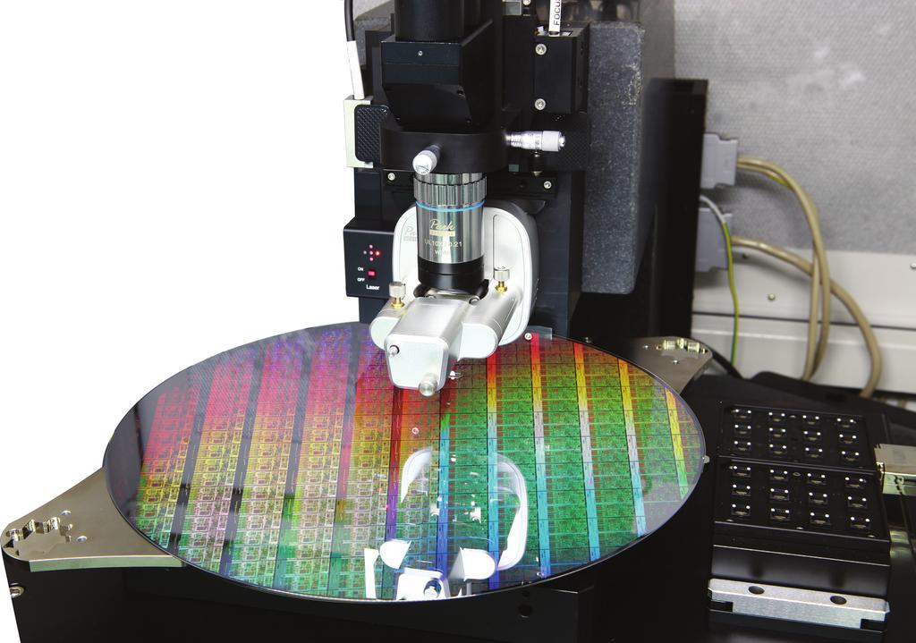
2 WAFER DEFECTS Article published in Issue Wafer defects can t hide from Park Systems Atomic Force Microscopy (AFM) leader Park Systems has simplified 300mm silicon wafer defect review by automating the process of obtaining high-resolution 3D images, making it faster and simpler than ever before. Figure 1: After coordinate mapping, ADR AFM will automatically perform a survey scan, zoom-in, processing, analysis and classification of each defect. SEMICONDUCTOR MANUFACTURERS have options for defect review once inspection tools have identified potential flaws on bare silicon wafers. While conventional AFM provides data-rich 3D images, the process is slow compared to 2D, SEM-based techniques. A new AFM process developed by Park Systems changes that equation like none other. Park Systems (Suwon, Korea and Santa Clara, California, USA) is one of the leading pioneers of atomic force microscopy (AFM) for semiconductor manufacturers and researchers. The company s founder (Sang-Il Park, PhD) led early efforts to commercialize the technology after being an integral part of AFM s development team at Stanford University in the 1980s. Park Systems made the extreme, high-resolution 3D imagery of AFM commercially practical, going on to develop products and software for surface roughness measurement in hard disk media that became an industry standard (the Park HDM series product family). Park s AFMs are also non-contact review tools, which eliminates the possibility of tool tips accidentally touching surfaces and possibly damaging wafers under review. While quality, data-rich images have been a hallmark of Park s AFMs from the beginning, this extreme quality came at the price of speed and simplicity. The company subsequently automated AFM scanning for disk media and has now brought a similar approach to reviewing defects of interest (DOI) on silicon wafers up to 300mm. Its hardware and software also support extreme ultraviolet (EUV) reticle photo masks, a critical step in creating future 450mm silicon wafers. Finding silicon wafer DOIs is challenging. All bare silicon wafers have a unique crystalline structure that is prone to small defects (Figure 1)that may be one nanometer or smaller. Manufacturers determine threshold sizes of interest along with shape and 20 Issue III 2016


3 WAFER DEFECTS Figure 2: Images collected via (a) standard vs. (b) enhanced vision of a bare silicon wafer with one small defect. The insets show magnified views. The small defect is easily observable in enhanced vision. Figure 3: Schematic of the process used to decorate crystal imperfections for defect inspection. depth characteristics that need attention. But while thresholds vary by manufacturer, it is clear that shrinking device geometries will impact whether defects once considered too tiny for concern could present problems for next-generation devices. There are a variety of laser light scattering techniques and process tools for inspecting wafers quickly, scanning hundreds or even thousands per hour. But inspection is just the beginning. A follow-up review by scanning electron microscope (SEM) or AFM takes inspection coordinates and zeros in on each location to image the defects. While SEM review is relatively quick, it cannot reveal much detail beyond a 2D image: a defect s X and Y dimensions. AFM goes much farther, creating X, Y and Z 3D images along with detailed topographic maps that further help identify and characterize an imaged DOI. AFM reveals defect details that SEM can routinely miss. Park s AFM defect review is highly accurate, which is a key ingredient for success in an industry that measures in microns and nanometers. The accuracy of their AFMs is so great that the company holds a roughly 90 percent share of the market for hard disk drive defect review systems. Whether the defect is on a silicon wafer or the surface of hard drive media, the key is how accurately the review device locates it and delivers the information needed for proper defect classification. SEM may give 22 Issue III 2016

4 WAFER DEFECTS a quick image, but it lacks the information that can be provided by AFM (see figure 4). As a reference tool, AFM is the go-to technology. Other AFMs can be a challenge to operate, so Park Systems addresses the problem with ADR: automatic defect review. We automated defect review and simplified it, so any technician can start the review process, and then simply walk away to do other tasks while the ADR AFM is operating, said Ardavan Zandiatashbar, PhD, Park s senior applications scientist. While different manufacturers have varying approaches to how they handle silicon wafer defects, all likely agree that better data about a particular defect determines whether it is serious enough to affect lithographic processing, or whether defects are so great in number and size that a wafer should be rejected outright. We started with hard drive media defect review. Manufacturers needed to know the source of defects for failure analysis purposes. While SEM can give a quick image, its image can t easily tell you if a defect is a pit or a bump or how tall or how deep it is. This is where AFM comes in; it helps you to identify and classify defects accurately and completely. We do what others cannot do, Zandiatashbar said. Wafer defects in Park s study typically fall into eight basic categories additional categories in different wafer surface reviews are possible. Some defects can t be classified at the inspection stage and may not fit into a typical category even after AFM review. But through AFM, the manufacturer will definitely know a defect s size and depth; they can apply their own standards to determine what actions should be taken. Many manufacturers want to use AFM routinely, but locating the defects and linking the AFM to inspection tools were critical issues previously. Results from conventional AFMs depend on the skill of the operator. We eliminated those issues by automating the process. Now, instead of reviewing just a few defects per day through laborious efforts and changing Figure 4: Defect review results with ADR AFM vs. SEM are shown. ADR AFM was able to locate and image all defects; SEM did not find defects 22 to 34. AFM and SEM images are rotated 180 degrees with respect to each other. Issue III

5 WAFER DEFECTS Figure 5: Defect classification based on the AFM data. numerous tool tips, Park s ADR AFM can image and fully characterize between four and 10 defects per hour. A technician can start ADR and let it run 24/7. Manual AFM review proceeds only as quickly as a skilled operator can function, he added. Park s ADR AFM is a turn-key solution. In addition to automating the review process, Park s non-contact approach to AFM does not alter the wafer s surface in any way, meaning every wafer reviewed can go onto further processing as needed. SEM-based review processes have another issue beyond quality of data. Their electron beams also have the potential to burn scan areas (see figure 6). This effect is typically more critical for photo-resist layers, but any disruption of a wafer s surface area can affect yield or other important factors. The differences in results obtained using Park Systems ADR AFM compared to SEM-based results are dramatic. In a test conducted by Park, a wafer containing surface defects was reviewed using both SEM and AFM-based techniques. The ADR AFM utilized was from Park s NX-WAFER family of products. 34 defects identified at the inspection stage were candidates for review. The first 21 defects were imaged by SEM, which delivered aerial, 2D views without sufficient information about the depth or outof-plane dimensions. The remaining 13 defects were not found by SEM despite identification during a laser light scattering (LLS) inspection (see figure 4). Park s ADR AFM was able to find all 34 defects. The SEM had found defects down to a certain size threshold; those imaged by ADR AFM were typically The differences in results obtained using Park Systems ADR AFM compared to SEM-based results are dramatic. In a test conducted by Park, a wafer containing surface defects was reviewed using both SEM and AFM-based techniques. The ADR AFM utilized was from Park s NX-WAFER family of products. 34 defects identified at the inspection stage were candidates for review Issue III 2016

.")
6 WAFER DEFECTS Figure 6: Comparison of data collected by SEM vs. ADR AFM. SEM shows a 2D, aerial view, while ADR AFM includes 3D data, thereby enabling a line profile, 3D construct and contoured colour scale. Figure 7: AFM image of a facet defect with several SEM burn-marks is shown; burns are marked by arrows. smaller or shallower than defects that the SEM could identify. The SEM also had issues identifying defects that had less edge sharpness, whereas the AFM in its automated scanning mode found everything (see figure 6). From the customer perspective, locating the defects of interest during the review process and determining size and depth can be critical. While SEM-based techniques can locate larger defects, it does not find them all and in fact missed 13 of 34 in this case. The lack of 3D information and SEM s inability to image the shallow and small defects matters to manufacturers. With Park s automatic defect review manufactures can have high quality 3D data of DOIs more quickly using a turn-key solution that any technician can operate, said Zandiatashbar. Automatic defect review from Park Systems maximizes productivity by up to 1,000 percent as reported by customers. But what satisfies customers most is the unprecedented level of accuracy including 3D imagery and detailed topographic information of even the smallest defects. With ever-shrinking semiconductor device geometries reaching beyond 14nm, defects critically impact microelectronic device performance. Park s approach to automating 3D imaging is revolutionary because it makes the benefits of AFM practical for leading device manufacturers and researchers pushing future product generation boundaries Angel Business Communications. Permission required Issue III 2016


7 2 μm x 2 μm Topography of MoS2 on SiO2 3 μm x 3 μm Failure analysis of contact plugs Power, Versatility, ease of use brilliantly combined for large sample AFM Park NX20 Accurate large sample AFM solution for research and FA laboratories Surface roughness measurements for media and substrates Large 300mm x 300mm sample size increases possibilities Defect review imaging and analysis High resolution electrical scan mode Accurate AFM topography with low noise Z detector 2 μm x 2 μm Topography of SRAM Device


8
The Most Accurate Atomic Force Microscope. Park NX-PTR Fully Automated AFM for Accurate Inline Metrology of Hard Disk Head Sliders.
 The Most Accurate Atomic Force Microscope Park NX-PTR Fully Automated AFM for Accurate Inline Metrology of Hard Disk Head Sliders www.parkafm.com Park Systems The Most Accurate Atomic Force Microscope
Abstract. Keywords INTRODUCTION. Electron beam has been increasingly used for defect inspection in IC chip
 Abstract Based on failure analysis data the estimated failure mechanism in capacitor like device structures was simulated on wafer in Front End of Line. In the study the optimal process step for electron
Auto classification and simulation of mask defects using SEM and CAD images
 Auto classification and simulation of mask defects using SEM and CAD images Tung Yaw Kang, Hsin Chang Lee Taiwan Semiconductor Manufacturing Company, Ltd. 25, Li Hsin Road, Hsinchu Science Park, Hsinchu
Perfecting the Package Bare and Overmolded Stacked Dies. Understanding Ultrasonic Technology for Advanced Package Inspection. A Sonix White Paper
 Perfecting the Package Bare and Overmolded Stacked Dies Understanding Ultrasonic Technology for Advanced Package Inspection A Sonix White Paper Perfecting the Package Bare and Overmolded Stacked Dies Understanding
Nanotechnology Solutions Partner
 Nanotechnology Solutions Partner Park Systems Corp. KANC F, Iui-Dong 96-1, Suwon, Korea 3-27 Tel. +82-31-56-68 Fax. +82-31-56-685 www.parkafm.co.kr Park Systems Inc. 3 Olcott St. Santa Clara, CA 955 Tel.
Advancements in Acoustic Micro-Imaging Tuesday October 11th, 2016
 Central Texas Electronics Association Advancements in Acoustic Micro-Imaging Tuesday October 11th, 2016 A review of the latest advancements in Acoustic Micro-Imaging for the non-destructive inspection
Characterization and improvement of unpatterned wafer defect review on SEMs
 Characterization and improvement of unpatterned wafer defect review on SEMs Alan S. Parkes *, Zane Marek ** JEOL USA, Inc. 11 Dearborn Road, Peabody, MA 01960 ABSTRACT Defect Scatter Analysis (DSA) provides
PROCEEDINGS OF SPIE. Classification and printability of EUV mask defects from SEM images
 PROCEEDINGS OF SPIE SPIEDigitalLibrary.org/conference-proceedings-of-spie Classification and printability of EUV mask defects from SEM images Wonil Cho, Daniel Price, Paul A. Morgan, Daniel Rost, Masaki
Nanotechnology Solutions Partner
 Nanotechnology Solutions Partner Park Systems Corp. KANC 4F, Iui-Dong 6-10, Suwon, Korea 443-270 Tel. +82-31-546-6800 Fax. +82-31-546-6805 www.parkafm.co.kr Park Systems Inc. 3040 Olcott St. Santa Clara,
Semiconductors Displays Semiconductor Manufacturing and Inspection Equipment Scientific Instruments
 Semiconductors Displays Semiconductor Manufacturing and Inspection Equipment Scientific Instruments Electronics 110-nm CMOS ASIC HDL4P Series with High-speed I/O Interfaces Hitachi has released the high-performance
Organic light emitting diode (OLED) displays
 displays") Ultra-Short Pulse Lasers Enable Precision Flexible OLED Cutting FLORENT THIBAULT, PRODUCT LINE MANAGER, HATIM HALOUI, APPLICATION MANAGER, JORIS VAN NUNEN, PRODUCT MARKETING MANAGER, INDUSTRIAL PICOSECOND
Ultra-Short Pulse Lasers Enable Precision Flexible OLED Cutting FLORENT THIBAULT, PRODUCT LINE MANAGER, HATIM HALOUI, APPLICATION MANAGER, JORIS VAN NUNEN, PRODUCT MARKETING MANAGER, INDUSTRIAL PICOSECOND
Wafer Thinning and Thru-Silicon Vias
 Wafer Thinning and Thru-Silicon Vias The Path to Wafer Level Packaging jreche@trusi.com Summary A new dry etching technology Atmospheric Downstream Plasma (ADP) Etch Applications to Packaging Wafer Thinning
B-AFM. v East 33rd St., Signal Hill, CA (888)
") B-AFM The B-AFM is a basic AFM that provides routine scanning. Ideal for scientists and educators, the B-AFM is capable of creating high-resolution topography images of nanostructures in standard scanning
B-AFM The B-AFM is a basic AFM that provides routine scanning. Ideal for scientists and educators, the B-AFM is capable of creating high-resolution topography images of nanostructures in standard scanning
Dektak II SOP Revision 1 05/30/12 Page 1 of 5. NRF Dektak II SOP
 Page 1 of 5 NRF Dektak II SOP The Dektak II-A is a sensitive stylus profilometer. A diamond-tipped stylus is moved laterally across the surface while in contact and measures deflections of the tip. It
NP-AFM. Samples as large as 200 x 200 x 20 mm are profiled by the NP-AFM system, and several stage options are available for many types of samples.
 NP-AFM The NP-AFM is a complete nanoprofiler tool including everything required for scanning samples: microscope stage, electronic box, control computer, probes, manuals, and a video microscope. Samples
Preface. The information in this document is subject to change without notice and does not represent a commitment on the part of NT-MDT.
 Preface The information in this document is subject to change without notice and does not represent a commitment on the part of NT-MDT. Please note: Some components described in this manual may be optional.
SPM Training Manual Veeco Bioscope II NIFTI-NUANCE Center Northwestern University
 SPM Training Manual Veeco Bioscope II NIFTI-NUANCE Center Northwestern University Introduction: Scanning Probe Microscopy (SPM) is a general term referring to surface characterization techniques that utilize
Nano-Imprint Lithography Infrastructure: Imprint Templates
 Nano-Imprint Lithography Infrastructure: Imprint Templates John Maltabes Photronics, Inc Austin, TX 1 Questions to keep in mind Imprint template manufacturability Resolution Can you get sub30nm images?
Inspection of 32nm imprinted patterns with an advanced e-beam inspection system
 Inspection of 32nm imprinted patterns with an advanced e-beam inspection system Hong Xiao, Long (Eric) Ma, Fei Wang, Yan Zhao, and Jack Jau Hermes Microvision, Inc., 1762 Automation Parkway, San Jose,
Layout Analysis Analog Block
 Layout Analysis Analog Block Sample Report Analysis from an HD Video/Audio SoC For any additional technical needs concerning semiconductor and electronics technology, please call Sales at Chipworks. 3685
Nanotechnology Solutions Partner
 Nanotechnology Solutions Partner Park Systems Corp. KANC 4F, Iui-Dong 6-10, Suwon, Korea 443-270 Tel. +82-31-546-6800 Fax. +82-31-546-6805 www.parkafm.co.kr Park Systems Inc. 3040 Olcott St. Santa Clara,
Flip Chip Solder Bump Characterization in 3D with X-Ray Microscopy. J. Gelb, A. Gu, L. Hunter, B. Johnson, and W.
 Flip Chip Solder Bump Characterization in 3D with X-Ray Microscopy J. Gelb, A. Gu, L. Hunter, B. Johnson, and W. Yun July 11, 2012 3D X-Ray Microscopy (XRM) Integrated Circuit Sample 3D XRM Data Set 1
High Repetition Rate USP Lasers Improve OLED Cutting Results
 Coherent White Paper May 7, 2018 High Repetition Rate USP Lasers Improve OLED Cutting Results High power ultraviolet, picosecond industrial lasers are widely employed because of their proven ability to
Focused Ion Beam System MI4050
 SCIENTIFIC INSTRUMENT NEWS 2016 Vol. 7 SEPTEMBER Technical magazine of Electron Microscope and Analytical Instruments. Technical Explanation Focused Ion Beam System MI4050 Yasushi Kuroda *1, Yoshihisa
ABSTRACT. Keywords: 3D NAND, FLASH memory, Channel hole, Yield enhancement, Defect inspection, Defect reduction DISCUSSION
 Yield enhancement of 3D flash devices through broadband brightfield inspection of the channel hole process module Jung-Youl Lee a, Il-Seok Seo a, Seong-Min Ma a, Hyeon-Soo Kim a, Jin-Woong Kim a DoOh Kim
Understanding & Optimising Scanning Electron Microscope Performance
 W Understanding & Optimising Scanning Electron Microscope Performance hilst the scanning electron microscope with the help of modern computing and sophisticated imaging systems has developed into an instrument
Quick Start ATOMIC FORCE MICROSCOPE West Campus Imaging Core
 Quick Start ATOMIC FORCE MICROSCOPE West Campus Imaging Core 1 Turn On the laser power 2 Open enclosure: - lift the door latch and open the enclosure door. 3 2 1 1.Unlock scanner: Lift the lever to the
Methodology for Trench Capacitor Etch Optimization using Voltage Contrast Inspection and Special Processing
 Methodology for Trench Capacitor Etch Optimization using Voltage Contrast Inspection and Special Processing 1 Oliver D. Patterson, 1 Xing J. Zhou, 1 Rohit S. Takalkar, 1 Katherine V. Hawkins, 1 Eric H.
SEMICONDUCTOR TECHNOLOGY -CMOS-
 SEMICONDUCTOR TECHNOLOGY -CMOS- Fire Tom Wada 2011/12/19 1 What is semiconductor and LSIs Huge number of transistors can be integrated in a small Si chip. The size of the chip is roughly the size of nails.
Failure Analysis Technology for Advanced Devices
 ISHIYAMA Toshio, WADA Shinichi, KUZUMI Hajime, IDE Takashi Abstract The sophistication of functions, miniaturization and reduced weight of household appliances and various devices have been accelerating
SEMICONDUCTOR TECHNOLOGY -CMOS-
 SEMICONDUCTOR TECHNOLOGY -CMOS- Fire Tom Wada What is semiconductor and LSIs Huge number of transistors can be integrated in a small Si chip. The size of the chip is roughly the size of nails. Currently,
Veeco Dektak 6M Profilometer
 Veeco Dektak 6M Profilometer System Ranges/Resolutions Range (Å) Resolution (Å) 50 (5nm) to 65K 1 0.5K to 655K 10 2K to 2620K 40 8K to 10000K (1mm) 160 Maximum sample thickness: 31.75mm Scan range: 50
An Overview of the Performance Envelope of Digital Micromirror Device (DMD) Based Projection Display Systems
 Based Projection Display Systems") An Overview of the Performance Envelope of Digital Micromirror Device (DMD) Based Projection Display Systems Dr. Jeffrey B. Sampsell Texas Instruments Digital projection display systems based on the DMD
An Overview of the Performance Envelope of Digital Micromirror Device (DMD) Based Projection Display Systems Dr. Jeffrey B. Sampsell Texas Instruments Digital projection display systems based on the DMD
Standard AFM Modes User s Manual
 Standard AFM Modes User s Manual Part #00-0018-01 Issued March 2014 2014 by Anasys Instruments Inc, 325 Chapala St, Santa Barbara, CA 93101 Page 1 of 29 Table of contents Chapter 1. AFM Theory 3 1.1 Detection
Nova NanoSEM Superior Imaging and Analytical Performance
 Nova NanoSEM Superior Imaging and Analytical Performance FEI Nova NanoSEM scanning electron microscopes combine best-in-class imaging with superb analytical performance in one easy-to-use instrument.
HOT LINKS Trade Show Schedule ISO Certification Contact
 July 2012 HOT LINKS Trade Show Schedule ISO Certification Contact Single-Field Scanning - Reduced Sensitivity To Contamination, Higher Quality PRODUCT SPOTLIGHT The type of scanning in harsh operating
Developing an AFM-based Automatic Tool for NanoAsperity Quantification
 Developing an AFM-based Automatic Tool for NanoAsperity Quantification September 18, 2008 Sergey Belikov*, Lin Huang, Jian Shi, Ji Ma, Jianli He, Bob Tench, and Chanmin Su Veeco Instruments Inc., Santa
EUV Mask and Wafer Defectivity: Strategy and Evaluation for Full Die Defect Inspection
 EUV Mask and Wafer Defectivity: Strategy and Evaluation for Full Die Defect Inspection Ravi Bonam 1, Hung-Yu Tien 2, Acer Chou 2, Luciana Meli 1, Scott Halle 1, Ivy Wu 2, Xiaoxia Huang 2, Chris Lei 2,
Electron Beam Technology
 Electron Beam Technology Best of both worlds: Direct write and direct view Ultra High Resolution Electron Beam Lithography and Scanning Electron Microscope Imaging MULTI TECHNIQUE ELECTRON BEAM LITHOGRAPHY
Revolutionary AOI Technology, Unbelievable Speed World's Fastest and Most Accurate 3D SPI
 Revolutionary AOI Technology, Unbelievable Speed World's Fastest and Most Accurate 3D SPI The Recognized Leader for Quality Inspection Solutions 1 WORLD'S FASTEST AND MOST ACCURATE 3D SPI 3 YEAR WARRANTY*
MILLENNIA. The Benchmark In Diode-Pumped Solid-State Lasers.
 MILLENNIA The Benchmark In Diode-Pumped Solid-State Lasers. Millennia.The Leader InHighPower Diode-Pumped Solid State Lasers. Unparalleled performance, unbeaten track record, and the largest installed
Explore the Art of Detection
 Y.Cougar Microfocus and nanofocus X-ray inspection systems for the electronics industries Explore the Art of Detection Technology with Passion Our specialty: The Art of Detection. Developing outstanding
Quick Start Bruker Dimension Icon AFM
 Do not remove Quick Start Bruker Dimension Icon AFM March 3, 2015 GLA Contacts Harold Fu (hfu@caltech.edu) Weilai Yu (wyyu@caltech.edu) Bruker Tech Support (AFMSupport@bruker-nano.com 800-873-9750) Watch
Press release. Among chips and ships. Aachen, May 21, International Laser Technology Congress AKL 08: Widening interest in luminous ideas
 Press release Aachen, May 21, 2008 Among chips and ships International Laser Technology Congress AKL 08: Widening interest in luminous ideas Over 30 years ago, the pioneers of laser technology would hardly
Reduction of Device Damage During Dry Etching of Advanced MMIC Devices Using Optical Emission Spectroscopy
 Reduction of Device Damage During Dry Etching of Advanced MMIC Devices Using Optical Emission Spectroscopy D. Johnson, R. Westerman, M. DeVre, Y. Lee, J. Sasserath Unaxis USA, Inc. 10050 16 th Street North
At-speed testing made easy
 At-speed testing made easy By Bruce Swanson and Michelle Lange, EEdesign.com Jun 03, 2004 (5:00 PM EDT) URL: http://www.eedesign.com/article/showarticle.jhtml?articleid=21401421 Today's chip designs are
UV Nanoimprint Tool and Process Technology. S.V. Sreenivasan December 13 th, 2007
 UV Nanoimprint Tool and Process Technology S.V. Sreenivasan December 13 th, 2007 Agenda Introduction Need tool and process technology that can address: Patterning and CD control Alignment and Overlay Defect
Overcoming Challenges in 3D NAND Volume Manufacturing
 Overcoming Challenges in 3D NAND Volume Manufacturing Thorsten Lill Vice President, Etch Emerging Technologies and Systems Flash Memory Summit 2017, Santa Clara 2017 Lam Research Corp. Flash Memory Summit
University of MN, Minnesota Nano Center Standard Operating Procedure
 Equipment Name: Atomic Force Microscope Badger name: afm Revisionist Paul Kimani Model: Dimension 3000 Date: October 1, 2013 Location: Bay 1 A. Description The Dimension 3000 consists of a rigid stage
24. Scaling, Economics, SOI Technology
 24. Scaling, Economics, SOI Technology Jacob Abraham Department of Electrical and Computer Engineering The University of Texas at Austin VLSI Design Fall 2017 December 4, 2017 ECE Department, University
Electron Beam Technology
 Electron Beam Technology Speed up! High Performance Electron Beam Lithography dedicated electron beam lithography To bridge cutting-edge research and nanofabrication, a dedicated nanolithography solution
Scaling up of the Iris AO segmented DM technology for atmospheric correction
 Scaling up of the Iris AO segmented DM technology for atmospheric correction Michael A. Helmbrecht, Ph.D., Min He, Carl Kempf, Ph.D., Patrick Rhodes Iris AO, Inc., 2680 Bancroft Way, Berkeley, CA 94704
X-ray Inspection. Series.
 X-ray Inspection Series www.nordsondage.com 2 Nordson DAGE Quadra X-ray Inspection 3 Nordson DAGE Quadra X-ray Inspection Nordson DAGE Quadra X-ray Inspection 3 Your X-ray Inspection Partner Seeing is
Application note. Materials. Introduction. Authors. Travis Burt, Huang ChuanXu*, Andy Jiang* Agilent Technologies Mulgrave, Victoria, Australia
 Performance of compact visual displays measuring angular reflectance of optically active materials using the Agilent Cary 7000 Universal Measurement Spectrophotometer (UMS) Application note Materials Authors
LEP400 Etch Depth Monitor Real-time, in-situ plasma etch depth monitoring and end point control plus co-linear wafer vision system
 LEP400 Etch Depth Monitor Real-time, in-situ plasma etch depth monitoring and end point control plus co-linear wafer vision system Base Configuration Etch Depth Monitoring LEP400 Recessed Window Plasma
Self Restoring Logic (SRL) Cell Targets Space Application Designs
 Cell Targets Space Application Designs") TND6199/D Rev. 0, SEPT 2015 Self Restoring Logic (SRL) Cell Targets Space Application Designs Semiconductor Components Industries, LLC, 2015 September, 2015 Rev. 0 1 Publication Order Number: TND6199/D
TND6199/D Rev. 0, SEPT 2015 Self Restoring Logic (SRL) Cell Targets Space Application Designs Semiconductor Components Industries, LLC, 2015 September, 2015 Rev. 0 1 Publication Order Number: TND6199/D
Digital Light Processing
 A Seminar report On Digital Light Processing Submitted in partial fulfillment of the requirement for the award of degree of Bachelor of Technology in Computer Science SUBMITTED TO: www.studymafia.org SUBMITTED
In-process inspection: Inspector technology and concept
 Inspector In-process inspection: Inspector technology and concept Need to inspect a part during production or the final result? The Inspector system provides a quick and efficient method to interface a
TT-2 AFM. This compact, second. generation tabletop Atomic. Force Microscope has all the. important features and benefits. expected from a light
 TT-2 AFM This compact, second generation tabletop Atomic Force Microscope has all the important features and benefits expected from a light lever AFM. For: Nanotechnology Engineers/Researchers Wanting
High ResolutionCross Strip Anodes for Photon Counting detectors
 High ResolutionCross Strip Anodes for Photon Counting detectors Oswald H.W. Siegmund, Anton S. Tremsin, Robert Abiad, J. Hull and John V. Vallerga Space Sciences Laboratory University of California Berkeley,
PRODUCT NEWS FEI LAUNCHES APREO HIGH- PERFORMANCE SEM RENISHAW OFFERS CONFOCAL RAMAN MICROSCOPE
 40 PRODUCT NEWS Larry Wagner, LWSN Consulting Inc. lwagner10@verizon.net FEI LAUNCHES APREO HIGH- PERFORMANCE SEM FEI (Hillsboro, Ore.) announced the new Apreo scanning electron microscope (SEM), offering
Results on 0.7% X0 thick Pixel Modules for the ATLAS Detector.
 Results on 0.7% X0 thick Pixel Modules for the ATLAS Detector. INFN Genova: R.Beccherle, G.Darbo, G.Gagliardi, C.Gemme, P.Netchaeva, P.Oppizzi, L.Rossi, E.Ruscino, F.Vernocchi Lawrence Berkeley National
Applied Materials. 200mm Tools & Process Capabilities For Next Generation MEMS. Dr Michel (Mike) Rosa
 Rosa") Applied Materials 200mm Tools & Process Capabilities For Next Generation MEMS Dr Michel (Mike) Rosa 200mm MEMS Global Product / Marketing Manager, Components and Systems Group (CSG), Applied Global Services
Applied Materials 200mm Tools & Process Capabilities For Next Generation MEMS Dr Michel (Mike) Rosa 200mm MEMS Global Product / Marketing Manager, Components and Systems Group (CSG), Applied Global Services
Durham Magneto Optics Ltd. NanoMOKE 3 Wafer Mapper. Specifications
 Durham Magneto Optics Ltd NanoMOKE 3 Wafer Mapper Specifications Overview The NanoMOKE 3 Wafer Mapper is an ultrahigh sensitivity Kerr effect magnetometer specially configured for measuring magnetic hysteresis
AIM INTRODUCTION SIMPLIFIED WORKFLOW
 CD-R PATENT PROTECTION: BRAND CHARACTERIZATION TO IDENTIFY COUNTERFEIT GOODS USING SIMPLIFIED MASS SPECTROMETRY James Morphet and Eleanor Riches Waters Corporation, Manchester, UK AIM To provide an easy-to-use
PROGRESS OF UV-NIL TEMPLATE MAKING
 PROGRESS OF UV-NIL TEMPLATE MAKING Takaaki Hiraka, Jun Mizuochi, Yuko Nakanishi, Satoshi Yusa, Shiho Sasaki, Yasutaka Morikawa, Hiroshi Mohri, and Naoya Hayashi Electronic Device Laboratory, Dai Nippon
Nikon s DigiMicro Position Encoders Nanometer Resolution with Sub-Micron Accuracy
 Nikon s DigiMicro Position Encoders Nanometer Resolution with Sub-Micron Accuracy Available in North America through NanoWave, Inc. The DigiMicro product line from Nikon is a family of optically-based
Advanced Display Manufacturing Technology
 Advanced Display Manufacturing Technology John Busch Vice President, New Business Development Display and Flexible Technology Group September 28, 2017 Safe Harbor This presentation contains forward-looking
Future of Analog Design and Upcoming Challenges in Nanometer CMOS
 Future of Analog Design and Upcoming Challenges in Nanometer CMOS Greg Taylor VLSI Design 2010 Outline Introduction Logic processing trends Analog design trends Analog design challenge Approaches Conclusion
AFM1 Imaging Operation Procedure (Tapping Mode or Contact Mode)
") AFM1 Imaging Operation Procedure (Tapping Mode or Contact Mode) 1. Log into the Log Usage system on the SMIF web site 2. Open Nanoscope 6.14r1 software by double clicking on the Nanoscope 6.14r1 desktop
AFM1 Imaging Operation Procedure (Tapping Mode or Contact Mode) 1. Log into the Log Usage system on the SMIF web site 2. Open Nanoscope 6.14r1 software by double clicking on the Nanoscope 6.14r1 desktop
De-embedding Techniques For Passive Components Implemented on a 0.25 µm Digital CMOS Process
 PIERS ONLINE, VOL. 3, NO. 2, 27 184 De-embedding Techniques For Passive Components Implemented on a.25 µm Digital CMOS Process Marc D. Rosales, Honee Lyn Tan, Louis P. Alarcon, and Delfin Jay Sabido IX
Cover Sheet. Scanning Report of Flexible Riser Pipe Section EVI /7/2005. Inspection Report
 Cover Sheet Document Number EVI-2005-0002 Document Date 7/7/2005 Document Title Customer -other- AEA Technologies Type Inspection Report Prepared by: Date: Reviewed by: Date: Approved by: Date: Evisive,
Supplementary Figure 1. OLEDs/polymer thin film before and after peeled off from silicon substrate. (a) OLEDs/polymer film fabricated on the Si
 OLEDs/polymer film fabricated on the Si") Supplementary Figure 1. OLEDs/polymer thin film before and after peeled off from silicon substrate. (a) OLEDs/polymer film fabricated on the Si substrate. (b) Free-standing OLEDs/polymer film peeled off
Supplementary Figure 1. OLEDs/polymer thin film before and after peeled off from silicon substrate. (a) OLEDs/polymer film fabricated on the Si substrate. (b) Free-standing OLEDs/polymer film peeled off
Advances in Roll-to-Roll Imprint Lithography for Display Applications Using Self Aligned Imprint Lithography. John G Maltabes HP Labs
 Advances in Roll-to-Roll Imprint Lithography for Display Applications Using Self Aligned Imprint Lithography John G Maltabes HP Labs Outline Introduction Roll to Roll Challenges and Benefits HP Labs Roll
Inspection of Imprint Lithography Patterns for Semiconductor and Patterned Media
 Inspection of Imprint Lithography Patterns for Semiconductor and Patterned Media Douglas J. Resnick, Gaddi Haase, Lovejeet Singh, David Curran, Gerard M. Schmid, Kang Luo, Cindy Brooks, Kosta Selinidis,
Next Generation of Poly-Si TFT Technology: Material Improvements and Novel Device Architectures for System-On-Panel (SOP)
") Next Generation of Poly-Si TFT Technology: Material Improvements and Novel Device Architectures for System-On-Panel (SOP) Tolis Voutsas* Paul Schuele* Bert Crowder* Pooran Joshi* Robert Sposili* Hidayat
Next Generation of Poly-Si TFT Technology: Material Improvements and Novel Device Architectures for System-On-Panel (SOP) Tolis Voutsas* Paul Schuele* Bert Crowder* Pooran Joshi* Robert Sposili* Hidayat
GMOS CCD Upgrade Options S. Kleinman, J. Jensen 26Sep08
 GMOS CCD Upgrade Options S. Kleinman, J. Jensen 26Sep08 Background We are planning to upgrade the scientific capability of GMOS-N by upgrading its roughly 10 year old E2V CCDs to newer CCDs with enhanced
DIRECT DRIVE ROTARY TABLES SRT SERIES
 DIRECT DRIVE ROTARY TABLES SRT SERIES Key features: Direct drive Large center aperture Brushless motor design Precision bearing system Integrated position feedback Built-in thermal sensors ServoRing rotary
Axle Assembly Poke-Yoke
 Indiana University Purdue University Fort Wayne Opus: Research & Creativity at IPFW Manufacturing & Construction Engineering Technology and Interior Design Senior Design Projects School of Engineering,
1. Publishable summary
 1. Publishable summary 1.1. Project objectives. The target of the project is to develop a highly reliable high brightness conformable low cost scalable display for demanding applications such as their
Owner's Manual LIGHTING CONTROL CONSOLE TEATRONICS LIGHTING CONTROLS, INC. PROCON II Los Osos Valley Rd., Ste. G Los Osos, CA 93402
 Owner's Manual PROCON II LIGHTING CONTROL CONSOLE TEATRONICS LIGHTING CONTROLS, INC. 1236 Los Osos Valley Rd., Ste. G Los Osos, CA 93402 Phone: (805) 528-6900 PROCON II FAX: (805) 528-9345 12/01/94 Page//
TT AFM LongBeach Procedures and Protocols V2.1
 TT AFM LongBeach Procedures and Protocols V2.1 1. Startup Procedure 1. Turn on PC: Allow to boot to Windows. Turn on monitor. Password is afm 2. Turn on second PC that controls the video camera. 3. Turn
Large-Scale Polysilicon Surface Micro-Machined Spatial Light Modulator
 Large-Scale Polysilicon Surface Micro-Machined Spatial Light Modulator Clara Dimas, Julie Perreault, Steven Cornelissen, Harold Dyson, Peter Krulevitch, Paul Bierden, Thomas Bifano, Boston Micromachines
Standard Operating Procedure of nanoir2-s
 Standard Operating Procedure of nanoir2-s The Anasys nanoir2 system is the AFM-based nanoscale infrared (IR) spectrometer, which has a patented technique based on photothermal induced resonance (PTIR),
Figure 1. MFP-3D software tray
 Asylum MFP-3D AFM SOP January 2017 Purpose of this Instrument: To obtain 3D surface topography at sub-nanometer scale resolution, measure contact and friction forces between surfaces in contact, measure
YXLON Cougar EVO PLUS
 YXLON Cougar EVO PLUS The best small footprint X-ray inspection system for LABORATORY applications Technology with Passion Choose a custom-built EVO solution for premium inspection Why compromise? As technology
A High-Speed CMOS Image Sensor with Column-Parallel Single Capacitor CDSs and Single-slope ADCs
 A High-Speed CMOS Image Sensor with Column-Parallel Single Capacitor CDSs and Single-slope ADCs LI Quanliang, SHI Cong, and WU Nanjian (The State Key Laboratory for Superlattices and Microstructures, Institute
Model-Based Mask Data Preparation (MB-MDP) and its impact on resist heating
 and its impact on resist heating") Model-Based Mask Data Preparation (MB-MDP) and its impact on resist heating Aki Fujimura* a, Takashi Kamikubo b, Ingo Bork a a D2S Inc., 4040 Moorpark Ave, Suite 250, San Jose, CA, 95117, USA; b NuFlare
Model-Based Mask Data Preparation (MB-MDP) and its impact on resist heating Aki Fujimura* a, Takashi Kamikubo b, Ingo Bork a a D2S Inc., 4040 Moorpark Ave, Suite 250, San Jose, CA, 95117, USA; b NuFlare
Connection for filtered air
 BeamWatch Non-contact, Focus Spot Size and Position monitor for high power YAG, Diode and Fiber lasers Instantly measure focus spot size Dynamically measure focal plane location during start-up From 1kW
Scanning Electron Microscopy (FEI Versa 3D Dual Beam)
") Scanning Electron Microscopy (FEI Versa 3D Dual Beam) This operating procedure intends to provide guidance for basic measurements on a standard sample with FEI Versa 3D SEM. For more advanced techniques
Scanning Electron Microscopy (FEI Versa 3D Dual Beam) This operating procedure intends to provide guidance for basic measurements on a standard sample with FEI Versa 3D SEM. For more advanced techniques
Scanning Probe Microscope Training. Wenhui Pang
 Scanning Probe Microscope Training Wenhui Pang Background - Comparison of AFM with Other Imaging Modalities Optical Microscopy SEM TEM AFM Resolution XY 200 nm 2 nm 0.1 nm 1 nm Z 500 nm N/A N/A 0.1 nm
Sealed Linear Encoders with Single-Field Scanning
 Linear Encoders Angle Encoders Sealed Linear Encoders with Single-Field Scanning Rotary Encoders 3-D Touch Probes Digital Readouts Controls HEIDENHAIN linear encoders are used as position measuring systems
ABSTRACT 1 INTRODUCTION
 Novel lithography technique using an ASML Stepper/Scanner for the manufacture of display devices in MEMS world ASML US, Inc Special Applications, 6580 Via Del Oro San Jose, CA 95119 Keith Best, Pankaj
An Alternative Architecture for High Performance Display R. W. Corrigan, B. R. Lang, D.A. LeHoty, P.A. Alioshin Silicon Light Machines, Sunnyvale, CA
 R. W. Corrigan, B. R. Lang, D.A. LeHoty, P.A. Alioshin Silicon Light Machines, Sunnyvale, CA Abstract The Grating Light Valve (GLV ) technology is being used in an innovative system architecture to create
EUV Blank Inspection
 EUV Blank Inspection J.H. Peters* a, C. Tonk a, D. Spriegel b, Hak-Seung Han c, Wonil Cho c, Stefan Wurm d a Advanced Mask Technology Center, Raehnitzer Allee 9, 01109 Dresden, Germany; b Siemens AG, Corporate
NDT Supply.com 7952 Nieman Road Lenexa, KS USA
 ETher ETherCheck Combined Eddy Current & Bond Testing Flaw Detector The ETherCheck is a combined Eddy Current and Bond Testing Flaw Detector which comes with a rich range of features offered by a best
9 rue Alfred Kastler - BP Nantes Cedex 3 - France Phone : +33 (0) website :
 website :") 9 rue Alfred Kastler - BP 10748-44307 Nantes Cedex 3 - France Phone : +33 (0) 240 180 916 - email : info@systemplus.fr - website : www.systemplus.fr January 2011 - Version 1 Written by: Sylvain HALLEREAU
9 rue Alfred Kastler - BP 10748-44307 Nantes Cedex 3 - France Phone : +33 (0) 240 180 916 - email : info@systemplus.fr - website : www.systemplus.fr January 2011 - Version 1 Written by: Sylvain HALLEREAU
MEMS METROLOGY USING A STROBED INTERFEROMETRIC SYSTEM
 XVII IMEKO World Congress Metrology in the 3rd Millennium June 22 27, 2003, Dubrovnik, Croatia MEMS METROLOGY USING A STROBED INTERFEROMETRIC SYSTEM Erik Novak, Der-Shen Wan, Paul Unruh, Michael Schurig
Figure 1: AFM image of a Tip-check sample
 Atomic Force Microscopy Atomic force microscopy is a microscope technique that involves viewing samples with a resolution of under a fraction of a nanometer. The applications for Atomic Force Microscopy
How UV selectable illumination inspection tool and methodologies can accelerate learning curve of advanced technologies
 How UV selectable illumination inspection tool and methodologies can accelerate learning curve of advanced technologies V. Twines, C. Archambuult, B. Hinschberger, E. Rouchouze ST Microelectronic Crolles