HMC TRAFFIC CONTROLLER
|
|
|
- Clifford Fisher
- 5 years ago
- Views:
Transcription


1 THE. PRODUCTS Rr:FERENCED HERt:N l\re NO LONGER MANUFACTURED BY HONEYWEll 1 THE RGHTS WTH REGARD THERETO HAV BEEN SOLD TO TRACONEX NC. HONEYWaL NC. S NOT RESPONSBLE FOR WARRAN11ES OR OTHER MAnERS CONCERNNG THE PRODUCTS HEREN REFERENcm..' HMC TRAFFC CONTROLLER Operation Manual Honeywell
2 HMC-1000 TRAFFC CONTROLLER OPERATON MANUAL Honeywell nc. TRAFFC M"ANAGEMENT CENTER 5121 Winnetka Avenue North New Hope, Minnesota /80 Printed in U. S. A. To reorder this manual, specify pn
3 [. Section APPENDX A APPENDX B TABLE OF CONTENTS CONTROLLER FUNCTONAL DESCRPTON Operational Specifications Modes Timing Man Sync (Stop Timing) Manual On Line Free (Local) Remote (Coordinated) Programmi.ng Signal Light and Control Sequences Sample PROM Programming Display and Front Panel Controls Power Up Condition External nputs Outputs THEORY OF OPERATON Controller Organization Dial Select Logic Memory Address Logic Programmer Connections Time Display Offset Logic Manual, On Line, Stop Time nputs Cycle, Offset, and nterval ;rimers Control Logic PROM nterval Display Power Supply Restart and Countdown Circuit Controller Subassemblies Mother Board and Programmer nput/output Board Display Card Memory Card Control Card Preempt Card Output Card Power Supply - SCHEMATCS, ASSEMBLY DRAWNGS AND PARTS LSTS - NCR 1105 EAROM OPERATON Page A- B-1 iii
4 SECTON 1 CONTROLLER FUNCTONAL DESCRPTON The Honeywell HMC-000 Traffic Controller (Figure 1-1) is a pre-timed intersection controller which operates in either an isolated or coordinated mode of operation. n the coordinated mode, the HMC-000 operates as part of a multi-dial interconnected system, either as a local intersection controller or as a combined local/master controller. The HMC-000 is capable of storing and timing four dials having up to 16 intervals each. Each interval can be programmed to switch 32 signal outputs into one of three user selected state conditions (On.. Off.. or Flash). The Controller has five modes of operation: Man Sync (Stop Timing), Manual, On-Line.. Free and Remote. The Free, Remote and Man Sync (Stop Timing) modes are selected from the front panel MODE switch on the HMC-OOO. The Manual and On-Line modes are selected through inputs to the HMC-000 entered through the nput /Output cable. The cycle, interval, dwell and offset times are easily programmed using the Honeywell HMCP-000 Programmer. The use of a non-volatile electrically alterable read-only memory (EAROM) assures the integrity of these stored operational parameters. Power failures or even physical disconnection and relocation of the controller have no effect on stored data. A visual display panel indicates the current controller operational status, and also provides visual verification of parameters entered into the EAROM. Programmable read-only memories (PROMs) are programmed to meet the specific signal input and output requirements of the controller application, and can be "burned-in11 at the factory or in the field using the HPP-000 Programmer. 1-1


5 Figure 1-1. Honeywell HMC-000 Solid State Traffic Controller 1-2
6 Figure 1-2 presents a block diagram of the HMC controller illustrating the various inputs, outputs and switch positions described in detail 'on the following pages. ( (1 [ 1.1 OPERATONAL SPECFCATONS Power Requirements: 95 to 135 Vac, 60 Hz, 0.75 amp max. Environmental: Temperature: - 30 F to 165 F. Heating and cooling supplied as part of terminal facilities., Humidity: 0 to 950/0, noncondensing. Electronic boards conformal coated. Physical: Height, 7. 6 inches; Width, 9.6 inches; Depth, 8 inches. Weight: 10 pounds. 1.2 MODES The HMC-lOOO operates in one of five modes as selected by the MODE switch and/or external inputs. f there is a conflict in the selection of one or more modes, the prevailing operational mode will be selected in the following priority Man Sync (Stop Timing), Manual, On-Line, Free, Remote Man Sync (Stop Timing) i n the Man Sync (Stop Timing) mode the HMC-1000 stops timing and holds in the current interval with the STOP TMNG indicator illuminated and the CLOCK indicator extinguished. The Man Sync mode is selected by grounding the STOP TME input through the nput /Output cable or by placing the MODE switch in the Man Sync position. 1-3
7 D SPLAY/PROGRAM DSPLAY ACTVE "\," r OFF 0 NTERVAL 0 CYCLE 0 DWELL OFFSET 1 0 OFFSET 2 0 OFFSET 3 0 ACTVE DAL REMOTE 0 1 _ ",." RESTART.. r OUTPUTS... STOP TME 32.. MANUAL.. 0- MANUAL ADVANCE LOGC AND... l./) ON LNE FOUR DAL - ADVANCE <ON LNE)... MEMORY => z p 24 VDC DAL 3... H.. p OFFSET MODE ON POWER o FREE REMOTE OFF 0 1 AMP o MAN SYNC FLASHNG... BUS Figure 1-2. HMC-1000 Controller Block Diagram 1-4
8 Manual ( [ n the Manual mode, the HMC-000 stops timing except for intervals that have been programmed to be guaranteed intervals. ntervals not programmed as such may be advanced one interval at a time by grounding the MANUAL ADVANCE input. ntervals may be programmed as guaranteed automatic advance or guaranteed manual advance required. ntervals programmed for guaranteed automatic advance will advance to the next interval when the programmed time has been reached. ntervals programmed for guaranteed manual advance will advance to the next interval only with manual advance. The Manual Advance mode is selected by grounding the MANUAL input through the nput/output cable. A MANUAL ADVANCE input before the programmed time has been reached causes the manual advance to be stored and the advance to occur at the programmed time. A MANUAL ADVANCE input after the programmed time has been reached causes the HMC-000 to advance to the next interval On Line [ t [ l [ n the On Line mode, the HMC-1000 functions in the same manner as in the Mar;ual mode except that the active input is the ADVANCE (ON LNE) input. The HMC-000 is placed in the ON LNE mode by grounding the ON LNE input through the nput/output cable. Note: The MANUAL and STOP TME inputs will override this input Free (Local) n the Free mode, the HMC-OOO times the intervals and automatically advances them without regard to external synchronization pulses. the Free mode when the MODE switch is in the FREE position. 1-5 The HMC-000 is in Synchronization
9 can be achieved even if the HMC-lOOO is not in an interconnected system. The controller can be placed in the Stop Timing mode by putting the Mode" switch in the MAN SYNC position for the appropriate time and then placing the MODE switch in the FREE position. The HMC- 100"0 will then operate in apparent synchronization because timing occurs by division of the 60Hz power line. Synchroni.zation is lost when power is interrupted Remote (Coordinated) n the Remote mode, the HMC-OOO times the intervals and automatically advances intervals in synchronization with synchronization pulses supplied to one of the OFFSET inputs. The HMC-OOO is ir:t the Remote mode when the MODE switch is in the REMOTE" position and synchronization pulses are being received. Synchronization is achieved by extending the dwell interval (assigned by PROM programming) for a time up to or equal to the programmed dwell time. Each time the dwell interval repeats, the interval is extended until synchronization is achieved. The dwell interval will then begin at the synchronization time, which is determined by delaying the incoming synchronization pulse by the offset time (stored in EAROM). Ftgure 1-3 illustrates the timing of an HMC-l 000 in synchronization when four intervals are used and interval 4 is.. the dwell interval. The offset time is programmable and may be any value between 0 seconds and the cycle time in one second increments. Figure 1-4 illustrates how the HMC-OOO achieves synchronization. These pulses are not recognized until the second synchronization pulse after the power and/or synchronization is turned on, or after the MODE switch is placed in the REMOTE position. The dwell interval is then extended by no more than the programmed dwell time until the controller is synchronized. ".. 1-6
10 ---n +GN24D OFFSET 11NPUT.. NTERVAL Figure 1-3. VDC J.--- CYCLE TME f.-- OFFS ET 1 T ME l3 --- n -... TME (SEC) Example of Synchronized HMC-1000 Utilizing Four ntervals (nterval 4 is dwell interval) FRST SYNCH PULSE RECEVED RECOGNZES SYNCH PRES ENT l! l OFFSET 1 NPUT NTERVAL HMC-1000 NOW SYNCHRONZED MODE FREE 1'41 REMOTE DWELL NTERVAL EXTENDED BY FULL DWELL TME '* DWELL NTERVAL EXTENDED BY LESS THAN FULL DWELL TME Figure 1-4. NTERVAL Example of HMC-1000 Detecting Synch Pulses and Extending Dwell nterval Until Controller is Synchronized (Note: Offset time is shown as zero) POSSBLE FUNCTON (3A CLEARANCE (3B GREEN (3B CLEARANCE (3A GREEN (DWELL NTERVAL) OFFSET 1 +24V NPUT OFFSET 2 NPUT +24V ---fl GND OFFSET 3 +24V NPUT n"' ----' TME (SEC)... GND n n ' "' OFFSET 2 OFFSET 3 * OFFSET 2 WLL SWTCH TO OFFSET 3 AT THE TME NDCATED F BOTH OFFSET 2 AND 3 ARE HGH FOR 100 MLLSECONDS. Figure 1-5. Offset Seection.1-7

11 Other features in the Remote mode include: f the synchronization should fail either high or low, the HMC-lOOO will revert to the Free mode without extending the dwell interval. n interconnected systems, in case the master controller fails or is temporarily removed from service, the HMC-lOOO will remain in synchronization as long as the other controllers in the system accurately track the 60Hz power line. Once the HMC-lOOO is in synchronization, it will remain in synchronization as long as the sync pulse cycle time is equal to the dial cycle time ±250ms. This feature is incorporated to allow the use of an electromechanical master controller which may introduce some jitter into the incoming pulses. f the sync pulse does not occur in this time frame, the HMC-OOO automatically extends the dwell (up to the maximum time set in the dwell timer) to try to obtain synchronization. The offset time may be selected as illustrated in Figure 1-5. Three offset times per dial may be programmed into the HMC-lOOO and selected by applying a synchronization pulse to the appropriate input. When the offset time is changed, the HMC-1000 will have to resynchronize itself. The HMC-lOOO can be used in a system that uses an offset interrupter. Some electromechanical timers require additional sync pulses, which often occur at random intervals between the regular sync pulses. The HMC-lOOO synchronizes only on pulses having the same cycle time as the HMC-lOOO is programmed for. CAUTON: f the master controller supplying synchronzationto the HMC-lOOO runs "fast" or has a slightly shorter cycle time, the HMC-lOOO will not synchronize or will not remain in synchronization. On the other hand, if the master runs" slower" or has a slightly longer 1-8
12 cycle time than the HMC-OOO, the HMC-OOO,will dwell in the dwell interval on each cycle and cause its cycle time to be extended to the master's cycle time. 1.3 TMNG t Timing may be programmed and stored in the EAROM for each dial within the limits shown below: MEMORY TME QUANTTY RANGE (SEC) NCREMENT (SEC) NTERVAL CYCLE DWELL O. 1 OFFSET The interval times control the amount of time the controller is in the interval. ntervals having zero time are skipped. Cycle" dwell, and offset times are used in the Remote mode as described above. t should be noted that the sum of all the interval times used must equal the cycle time and therefore the sum of all the interval times must be measured in 1 second increments. The HMCP-000 Programmer has circuitry that assures this relationship. Figure 1-6' illustrates a chart format that can be used to program the HMC-000. Mark the times for the dwell interval and the last interval, then fill in all the times for the dials and intervals used. This chart can be used for programming and maintaining records. Timing is derived from the 60 Hz power line by applying threshold detection, hysterisis" and filtering to the 60 Hz waveform (for noise rejection) and then dividing the frequency by digital counters to 10 Hz and 1 Hz. The 10 Hz signal drives countdown circuitry, and the 1 Hz signal drives flashing displays and flashing signal circuits. 1-9
13 cn O' co coo -'. NTERVAL TYPE (f) l1j «$... c TME (SEC) DAL 1 DAL 2 DAL 3 DAL 4 NTERVAL ',1 CYCLE 2 _ _0- _. - _0- -'- 4 _0- _.- _ _ 5 _.- _. - _. - _. - 6 _. - _. - _. - _.- 7 _. - _.- _. - _.- 8 _. - _ _. - _ _ -.- _ _.- _.-._.- _.- 12 _ _.- _ _ _ _.- 15 _0.- _.- _ \V V1\ DWELL OFFSET 1 OFFSET 2 OFFSET 3 Figure 1-6. HMC-1000 Controller Programming Chart
14 1. 4 PROGRAMMNG SGNAL LGHT AND CONTROL SEQUENCES The three state conditions (On, Off, Flash) of the 32 outputs and 8 interval control functions can be programmed for each interval. Programming is accomplished by "burning" metal links on fi ve programmable read only memory (PROM) chips using an HPP-000 Programmer or equi valent. The PROM's are then inserted into sockets on the HMC-000's Output Card. Each PROM controls 8 outputs or internal control functions. Figure 1-7 illustrates how the PROM's are organized and is a chart to aid in programming the HMC t is not necessary to insert all five PROM's in an HMC-000 but PROM 1 is always required. The flashing state is one flash per second, with a 50 percent duty cycle. For ready reference the function of each output can be defined on Figure 1-7 in terms of cabinet wiring, for example: Output 1, controlled by PROM 1, Bit 0, could be Phase-A Red; Output 2, controlled by PROM 1, Bit 1, could be Phase-A Yellow; etc. As is evident from the figure, some of the PROM bits are permanently assigned to interval control functions of the HMC-000. These permanently assigned control functions are described below. None of the control functions operate in the flash state. LAST NTERVAL - A logic 1 is inserted in the last interval. For example, if 13 intervals are required a 1 in interval 13 will cause the HMC-000 to skip intervals 14, 15, and 16 jump to interval 1 after interval 13. f more than one interval is programmed as last interval, the lowest numbered last interval will be considered the last interval. DWELL NTERVAL - A logic 1 is inserted in the dwell interval. For example, if interval 10 is to be the dwell interval (possibly main street green), a 1 is inserted in interval 10. For successful 1-11
15 FUNCTON f- >- :::> NTERVAL o <X: :2 a. <X:...J 0!:: f- ow a:: :::> co...ja:: a LAST NTEVAL * 6 DWELL NTERVAL * GUARANTEEDNTERVAL* 2 WTH AUTO ADVANCE * GUARANTEED NTERVAL* 3 WTH MAN ADVANCE * ALLOW DAL TRANSFER * 4 SPECAL 1 * 5 SPECAL 2 * 6 SPECAL 3 *, 7 1 = LGHT ON o OR BLANK = LGHT OFF F = FLASHNG * = FLASHNG STATE NOT ALLOWED FOR THS BT J 0 =ACTVE =NOT ACTVE Figure 1-7. PROM Program Sheet 1-12
16 coordinated operation, only one interval may be the dwell interval. GUARANTEED NTERVAL WTH AUTOMATC ADVANCE - This feature is active only in the Manual or On Line modes and is typically used to guarantee adequate clearance time in these modes. During Manual or On Line modes, the intervals having 0 for this bit will time out and automatically advance to the next interval wtth or without a manual advance or computer advance input. ntervals having 1 for this bit and 1 for the Guaranteed nterval With Manual Advance bit will cause stop timing and require a manual (or computer) advance to go to the next interval f a PROM is not plugged into the PROM 5 socket, all intervals will require manual advance. f a new but unprogrammed PROM is plugged into the PROM 5 socket, all intervals will time out and automatically advance, if in the Manual or On Line modes, and the HMC-OOO will appear to be in the Free mode. (Unprogrammed PROMs have all bits set to 0.) ntervals programmed with 0 for this bit and the other guaranteed interval bit will time out and automatically advance in the Manual and On Line modes. GUARANTEED NTERVAL WTH MANUAL ADVANCE - This feature is active only in the Manual or On Line modes and is typically used to extend the length of movements but guarantees a minimum time for the movement. n the Manual or On Line mode, the intervals having 0 for this bit will be timed and held until a manual (or computer) advance is received. (During the Manual mode only manual advance commands are accepted.) f the advance command is received before the programmed time, the advance will be remembered and the interval advanced when at the end of the programmed time. f an interval is:.inadvertently programmed for both options it will require a manual (or computer) advance to go to the next interval. 1-13
17 ALLOW DAL TRANSFER - When this bit is 1, remote transfer of the dial is allowed. When this bit is 0, remote transfer of the dial is inhibited. Typically this feature is used to permit dial transfer during one or more selected intervals. No PROM in the PROM 5 socket causes all intervals to allow dial transfers. An unprogrammed PROM in the PROM 5 socket results in no remote dial transfers allowed. Special 1, 2, 3 are unused bits reserved for special functions Sample PROM Programming Figure 1-8 illustrates a PROM Programming Sheet filled out to reflect the programming sequence required to prepare an HMC-1000 Traffic Controller for proper operation. The format illustrated is for a 2-phase intersection with pedestrian signals. n this example, nterval 1 is vehicle clearance, showing yellow on the main street signal. nterval 2 is an all red clearance. nterval 3 is the side street movement, with side street green and walk illuminated. nterval 4 is side street pedestrian clearance, with the side street flashing don't walk. nterval 5 is side street yellow clearance followed by nterval 6, all red clearance. nterval 7 is a main street movemnt, with main street showing green and walk, followed by pedestrian clearance, nterval 8 (flashing don't walk). nterval 7 is defined by PROM 1 to be the dwell interval that is extended when the HMC-1000 Controller is synchronizing itself in a coordinated system. nterval 8 is the last interval, this means that intervals "9 through 16 are skipped. 1-14
 0 0 0 \"'1tJ 'ST. 4CW 'G 3 2 0 0 0 0 0 0, ld 'ST. ttl: D 'Zit 4 3 0 0 0, SlOe ST. 'e\.?y \" 5 4 0 0 0, 0 0 0 S,'tl ST.-t;.Rtol \"Z.")

 26 3.r- '\ C.")
 0 0 32 1 0 0 0 0 0 0 0 0 0 0 (;) (;) 0 0 \" ALLOW DAL TRANSFER* 4 0 0 0 0 0, 0 SPECAL 1 * 5 0 0 0 0 0 0 \" 0 SPECAL 2 * 6 0 0 0 0 0")


18 FUNC.ON - >- NTERVAL ::J ::;; 0«Q. 0 -!:: «-l - ow ::J co '" Q. -l'" halt-) T. eo \ \, \ \ 0 0 """U T. 'E. L. \y 2, C) "'1tJ 'ST. 4CW 'G , ld 'ST. ttl: D 'Zit , SlOe ST. 'e\.?y " , S,'tl ST.-t;.Rtol "Z.G C LAST NTEVAL * DWELL NTERVAL * MAl\.! T. t).w. ' ,, 0 MAl'" T. C.W '3V AW!iT. -.,AL.J,13Ca SlOE ST. D.W. 4R 10 3,, 0, SOE-ST.O,W. 4Y <:> 'OE ST. Wit"'" fij(; l"\ ; \.11 1 t-\ h.. F.-J' D \... " V 19 4,.., - """ 20 5,,,"1\',f\ -... (; 21 6 r.l \." \ 18 3 v l y, A" ( ') 26 3.r- '\ C.J h 28 5 j 27 4 "'lj GUARANTEED NTERVAL* 2 WTH AUTO. ADVANCE * GUARANTEED NTERVAL* 3 WTH MAN. ADVANCE * " (;) (;) (;) 0 0 " ALLOW DAL TRANSFER* , 0 SPECAL 1 * " 0 SPECAL 2 * SPECAL 3* = LGHT ON o OR BLANK = LGHT OFF F = FLASHNG * = FLASHNG STATE NOT ALLOWED FOR THS BT " 0 t. NTERVAL 1 NTERVAL 2 NTERVAL 3 NTERVAL 4 NTERVAL 5 NTERVAL 6 NTERVAL 7' NTERVAL 8 MS SS MS SS MS SS MS SS MS SS MS SS MS SS MS SS R a 0 0 a G () 0 () W y NTERVAL 9 NTERVAL 10 NTERVAL 11 NTERVAL 12 NTERVAL 13 NTERVAL 14 NTERVAL 15 NTERVAL 16 MS SS MS SS MS SS MS SS MS SS MS SS MS SS MS SS R y G OW W OFF.. - : } l'notact'" 0= ACTVE.- ON () - FLASHNG Figure 1-8. PROM Programming Sheet (Sample Program) f-15
19 r Note that PROM 5 defines nterval 7 as the only interval allowing dial trans-, fers to occur, and that all intervals except 3 and 7 are Guaranteed ntervals with Automatic Advance when the HMC-1000 Controller is in the On-line or Manual Mode. ntervals 3 and 7 require manual advance and they are not guaranteed since they are not clearance intervals DSPLAY AND FRONT PANEL CONTROLS Referring to Figure 1-1, the Display indicates the active interval on the selected dial, the selected time for that interval, and the status of the HMC The NTERVAL display is a two digit number (1 through 16) and the TME!SEC display is a three digit number with decimal point. The time displayed is selected by the DSPLAY!PROGRAM switches. The upper switch; ACTVE, 1, 2, 3, 4 selects the dial being displayed. The ACTVE position displays information selected by the ACTVE DAL switch. The ACTVE DAL and DSPLAY!PROGRAM switches do not have to be in the same positions. -The lower DSPLAY!PROGRAM switch selects the type of data being retrieved from EAROM and being displayed. n the OFF position the NTERVAL and the TME!SEC displays are extinguished. To lengthen their life it is recommended that the displays be turned off during normal operation and be turned on only when troubleshooting or when programming is being performed. n the NTERVAL position, the current interval is displayed arid the stored. interval time is displayed. (When programming, the interval being programmed and its time are displayed independent of the currently operating interval.) n 1-17
20 the other positions the function times are displayed. This switch is also used to select what functions are being programmed when an HMCP-1000 Programmer is used for programming. The other status displays operate continuously. 1. The STOP TMNG indicator is illuminated when the HMC-1000 is not timing. 2. The CLOCK indicator flashes at one flash per second when the controlle r is timing. 3. The OFFSET indicator indicates which one of the three offsets is being used. 4. The DAL indicator indicates which one of the four dials is currently active. The ACTVE DAL switch, REMOTE, 1, 2, 3, 4, selects the currently active dial that the controller is operating in. REMOTE allows the remote input lines to select the dial, subject to the Allow Dial Transfer bit. The other positions select a dial without regard to the Allow Dial Transfer bit. NOTE: The current interval time being timed does not change immediately when the ACTVE DAL switch is changed. The timer reads a new time only when it completes the current interval period. This procedure prevents any out of step operation when switching dials. The display may indicate a time from one dial while the controller is timing a time from a previously selected dial. p.
21 The MODE switch selects the REMOTE, FREE, or MAN SYNC (stop timing) modes according to the function description in paragraph The POWER switch supplies the 115 Vac power to the HMC slow blow fuse protects the HMC-OOO. A 1 ampere The NPUT /OUTPUT connector connects the HMC-1000 to the cabinet wiring and includes all inputs, outputs, and 115 Vac power. The PROGRAMMER connector allows connection of the HMCP-1000 Programmer or other suitable programmers to program the timing functions POWER UP CONDTON When power is first applied to the HMC-1000, the following initial conditions occur: 1. The interval is set to The ACTVE DAL switch selects the dial. f the ACTVE DAL switch is in the REMOTE position, the dial is selected by external input. 3. Timing begins approximately O. 5 second after power is applied. This delay assures that all power supply voltages are within tolerance before starting operation. 4. The HMC-OOO powers up in the Free mode unless it is in the Manual, On Line, or Man Sync modes. 5. f external offset signals are present the correct offset is selected before sync is recognized. 1-19
22 For power interruptions of less than 500 milliseconds, the HMC-1000 will retain the current interval and, when power is reapplied, operation will commence without resetting. During the power interruption, the timer will stop timing since the 60 Hz signal is not present. n a coordinated system a power loss may cause synchronization to be lost if the power interruption did not also occur at the master controller. For power interruptions of greater than 1 second, the HMC-1000 will reset to the power up condition when power is reapplied. For power interruptions between O. 5 and 1 second, either reset or continued operation may occur EXTERNAL NPUTS This paragraph describes the functions of the external inputs (see Figure 1-2). 1. DAL 2, DAL 3, and DAL 4. These inputs select the active dial when the ACTVE DAL switch is in the REMOTE position. Grounding one of these inputs selects the appropriate dial. f none of these inputs are grounded, Dial 1 is selected. f more than one dial input is grounded, the highest number dial is selected. 2. OFFSET 1, OFFSET 2, OFFSET 3. These inputs provide synchronization and offset selection as described in paragraph Grounding more than one input will result in the controller operating in the Free mode. f one input is continuously grounded while the other input has a sync pulse an unknown offset selection will result if more than one input has "simultaneous 11 sync pulses. 3. RESTART. Grounding the restart input holds the HMC-1000 in the power up restart condition described in paragraph When the restart input is released, the HMC-1000 will start running. 1-20
23 4. STOP TME (man sync), MANUAL and MANUAL ADVANCE, ON LNE, ADVANCE, See paragraphs , , and , respectively, for a description of these inputs VAC, NEUTRAL, and CHASSS GND. These are the 60 Hz 115 Vac power connections for the HMC Vac input is the "hot" side of the power line anc should be connected to the"colored, " ungrounded wire as specified by the National Electrical Code. The NEUTRAL input is the grounded side of the power line and should be connected to the white wire as specified by the National Electrical Code. The CHASSS GND connects to the HMC-1000 chassis and is a safety ground to prevent the unit from becoming "hot" should there be a failure in the insulation between the Vac and chassis. The CHASSS GND should be connected to the cabinet at the terminal facilities. 6. LOGC GND. Several logic ground pins are available on the HMC-1000 NPUT /OUTPUT connector. The LOGC GND is the reference for all inputs and outputs (except 115 Vac power) and is not connected to the chassis ground. The electrical requirements for the external inputs are listed in Table
24 , 0)'" o' col:" col:" Table 1-1. Electrical Requirements for External nputs TRDE (ON). APPROXMATE PULL UP PULL UP COND- MAX SNK FALSE (OFF) DELAY BEFORE FUNCTON RESSTOR TO TON CURRENT CONDTON OPERATE (K OHMS) (VOLTS) (VOLTS) (MA) (VOLTS) (milliseconds),dal o to to DAL o to to DAL o to to OFFSET o to to OFFSET o to to OFFSET o to to ON LNE o to to ADVANCE (on line) o to to MANUAL o to to MANUAL ADVANCE o to to STOP TME o to to RESTART o to to to 100
25 '. 1.8 OUTPUTS This paragraph describes the functions of the outputs from the HMC OUTPUTS 1 THRU 32. These outputs are designed to drive solid state load relays and are the 32 outputs intended to control signal lights, sync pulse (when HMC-1000 is used as a master), or other control functions. These outputs are programmable as described in paragraph FLASHNG BUS. This is a general purpose output that supplies a 24 VDC, one flash per second, 50 percent duty cycle output VDC. This output is regulated 24 VDC for the load relays and for the conflict monitors. CAUTON: THS OUTPUT SHOULD NOT BE SHORTED TO GROUND. SEROUS DAMAGE TO THE HMC-1000 COULD RESULT F THS OUTPUT S SHORTED TO GROUND. 1-23,
26 ELECTRCAL CRCUT REQUREMENTS FOR HMC-1000 OUTPUTS +24 ± 1 VOLTS OUTPUT 1 THROUGH 32 10K OHMS 10 OHMS ""t:--...j\rvv' Vee J OUT PU T.- SNK LOGC GND MAXMUM SNK CURRENT =40 ma MAXMUM VOLTAGE (APPLED TO OUTPUn =30 VOLTS MAXMUM VCE SATURATON VOLTAGE =0.7 VOLT OPTONAL OUTPUT 1 THROUGH OHMS..,,---r-.JV'o,N'---+ OU T PU T.- SNK MAXMUM SNK CURRENT =100 ma MAXMUM VOLTAGE (APPLED TO OUTPUn =24 VOL TS MAXMUM VCE SATURATON VOLTAGE =1.1 VOLTS FLASHNG BUS 200 OHMS 10 OHMS FLASHNG BUS LOGC GND MAXMUM OUTPUT CURRENT = 25 ma APPROXMATE ON RESSTANCE = 220 OHMS APPROXMATE OFF RESSTANCE (GREATER THAN 100 K OHMS) +24 VDC VOL TAGE TOLERANCE: 24 ± 2 VOLTS DC MAXMUM CURRENT: 0.18 AMPERES CAUTON: SEROUS DAMAGE TO THE HMC-1000 COULD RESULT F THE +24 VDC OUTPUT S SHORTED TO GROUND
27 SECTON 2 THEORY OF OPERATON The high operational reliability of the all solid state HMC-1000 Controller is achieved through the extensive use of low-noise CMOS circuitry. HMC-1000 meets NEMA specifications fop all defined input and output signal levels and environmental requirements. Figure 2-1 illustrates the HMC-1000 Controller's organization by function. An electrically alterable read only memory (EAROM) and support addressing and timing logic stores the interval, cycle, dwell and offset times while a programmable read only memory (PROM) stores the state of each output (On, Off, Flash) for each interval. Digital countdown timers measure the cycle time, offset time, interval and dwell time using data stored in the EAROM and based on the 60Hz line frequency. dwell in the Remote Mode, back to nterval 1 (after the last interval), etc. The Control logic decides when to when to advance the interval counter, when to skip The control logic also controls the advance interval in the On Line, and Manual modes controlled by appropriate inputs. Dial select logic selects the active dial from the ACTVE DAL switch or from remote inputs and selects the dial to be displayed or programmed from the DSPLAY!PROGRAM switch. Offset logic detects synchronizationpulses from the three offset input lines. active DAL, Displays indicate NTERVAL, TME, active OFFSET, CLOCK, and STOP TMNG. The power supply distributes power to all HMC-1000 circuits, th. external cabinet functions, and the HPP-1000 Programmer. 24 Vdc to A power up reset and clock circuit initiates the interval counter and the flip flops in the control logic. 2-1
28 CONTROL, ADDRESS, DATA TO PROGRAMMER o. Cl) CO co Vl :::> Cl. 2 2 :i 3 Ci 4 LJ. Vl Ll.. Ll.. o y t «-.....,... f...,... «OFF 0 o f----t...j NTERVAL-- ACTVE CYCLE 0 -<> DWELL 0 0 STROBE «TME > NTERVAL DSPLAY 0:: LJ. DSPLAY - 2 OFFSETl 0 2 «<.:l 3 OFFSET20 2 -<> -<.:l OFFSET3 0 ::;;;0 i.o t=...j >,Vl - o::::;;;vl NTERVAL --. oolj. PROM <32> ::;;;0::0:: DAL LJ.«: DAL SELECT ::;;;«...J 0 1 LOGC ADDRESS 0:: - (CAM) 2 A 0 CTVE DAL. u CONTROL '...J Vl«REMOTE 0 0::> L-t DAL, LJ.0:: 1-<> OFFSET, ::;;;LJ. RESTART CLOCK 1- PWR UP 2 AND STOP 2- RESET :;:0 TME LED MODE 10Hz fand CLOCK :: CRCUT 4-0 O«LJ. FREE 0 -Ul- 2_2 :::><.:l:::> REMOTE OFFSET U...JU OFFSET MAN SYNC 0 2 LOGC SYNC 3 OUTPUT ( ON LNE, ADV. MAN. MAN. ADV. STOP TME 24VDC POWER TO PROG. / POWER SUPPLY R 115VAC RESTART Figure 2-1. HMC-1000 Controller - Organized by Function
29 Numerous connections to the HPP-1000 Programmer supply control timing and data flow between the two units. 2.1 CONTROLLER ORGANZATON The memory used to store time data in the HMC-1000 Controller is an EAROM, organized as a 256 word, four bit word device. A word may be addressed by selecting one of 8 row inputs and any combination on 5 column inputs (the column input address is decoded on the EAROM chip to select one of 32 columns). A word may be written or read, one 4 bit word at a time, by selecting the row and column address and applying proper timing signals to clock inputs. The data when read appears at the 4 bit data input/output terminals. When writing data, the data at the input/output terminal, driven by the programmer, will be stored in memory. The erase operation must have occurred before writing data. This is accomplished by putting a high voltage (+54 volts) pulse on a selected row line. The entire row is erased at one time. n the HMC-1000, two rows (containing 64 words) are used for one dial. Erasing, accomplished only when a programmer is connected to the HMC-1000, erases two rows at a time which corresponds to erasing one dial at a time. A memory chip is capable of storing the timing data for 4 dials. For more information on the EAROM see Appendix B. 2-3
30 " Each 4 bit word in the memory corresponds to a decimal digit and is. encoded as a Binary Code decimal number as shown below: Bit Decimal Displayed D3 D2 D1 DO Value Character Not Valid A Not Valid - (minus sign) Not Valid C Not Valid (dark or blank) Not Valid E Not Valid F Notice that the combinations above decimal value 9 are not valid decimal numbers but that characters having invalid decimal values may be displayed by the seven-segment time displays as a alphabetic or other characters. During normal operation the programmer enters only valid decimal values into mmory but when the memory is erased, some of the data read out of the erased memory will be invalid decimal numbers. Three four bit words are used to make up a 3 digit time display. Each dial contains; 16 - three digit interval times, 1 - three digit cycle time, 1 - three digit dwell time and 3 - three digit offset times. Each dial requires 63 words to store the above time information. 2-4
31 t f 1 J Timing is done in the HMC-OOO using presetable counters as illustratd in Figure ::: UJ Z ;:) o uo <C ọ.j L BT DATA FROM MEMORY CLOCK At the beginning of the period to be timed, one digit at a time is retrieved from EAROM and loaded into the counters. digit 1, then counter 1 is loaded. 2-5 First memory is addressed for Then in a similar manner, the other two digits are loaded into the counters with data from memory. approximately 2 ms., r-t DWN BORROW. r TME OUT counts the three counters down.,... p COUNTER 1 COUNTER 2 COUNTER 3 Figure Loading takes A clock, derived from the 60 Hz power line, then When all three counters contain zero, a time out pulse is generated terminating the timed period. f the clock frequency is 1 Hz, the range of timing is 0 to 999 seconds in 1 second increments. f the clock frequency is 10Hz, the range of timing is 0 to 99.9 seconds in O. 1 second increments. Countdown Circuit
32 Since tp.ere :are several counters, a display, and a programmer that must read or write data, the EAROM must be time shared among the several users. Timing logic is used to multiplex the EAROM addressing and data routing to the several users. Figure 2-3 is a detailed block diagram of the HMC-1000 showing all connections to the programmer (--7- r ), all inputs (0--) and. outputs ( [J-:-). One line on this block diagram may represent several wires, for example (4). represents four wires. The block diagram also indicates which card or cards contain the function described in the block diagram Dial Select Logic Starting from the left in Figure 2-3, the dial select logic selects the active dial (controlling the signal lights) and the dial to be programmed or displayed. Remote dial inputs are first buffered and filtered and prioritized. For example, if dial 4 and dial 3 inputs are low, dial 4 is selected. The remote dial input is then buffered by a 4 bit latch that holds the dial until the transfer allow bit from the PROM is set. When the ACTVE DAL switch (S3) is in the REMOTE position, the active dial selected is the dial stored in the 4 bit latch. When the ACTVE DAL switch is in any other position, the active dial selected is by the switch. The DAL display LED's display the active dial. The DSPLAY/PROGRAM switch (82) selects the dial to be displayed which may be the active dial displayed by the dial display LED's or one of the other three dials. The output of the dial select logic is multiplexed depending on whether data is being loaded into counters (active dial) or into the display (display/program dial). J': 2-6
33 , O *'" en t\:) CO -.;j CO DSPLAY/PROGRAM SWTCHES ACTE DAL 2 DAL 3 DAL 4 OFFSET 1 BUFFERS S2 S1 u. u. o >- -' «>- w -' u C >- :5 Cl 0 Cl c::: :oj '"'TN NTERVAL CYCLE DWELL OFFSET 1 OFFSET 2 OFFSET TART OFFSET LOGC :;J.... z o u ::; '" '" '"o «::; '" > Y 0 ;:; J+ SYNC PULSE V> '" w '"o ou «<:;; ",-, >-0 o ::; 1- {,,-3;..' 2 ON LNE L_...:=::..::.. ti5 - RESTART KEY f----t 0 w <D w '" i U ' in,..:...,.,. 21 i 5i u w w V>... «0: <:;...,. c; «0 LOAD DWELL MEMORY (EAROM> TO PROGRAMMER -- FROM PROGRAMMER NPUT OUTPUT CONNECTON TO ANOTHER PLACE ON PAGE CONNECTON FROM ANOTHER PLACE (3) (3) NDCATES NUMBER OF WRES ----;> --< er a- V> 0. t;: ADVANCEi.ON 00 LNE) MANUAL (CARD 4> START o RESTART 60 Hz CKT (2) NTERVAL NUMBER, CARD 3) OR (2), NDCATES CRCUT ON CARD SPECFED 1 (CARD 21 v :i: t---f DSPLAY OFF 10 Hz CLOCK CARD NO. CARD NAME 1 DSPLAY 2 MEMORY 3 CONTROL 4 PREEMPT 5 OUTPUT 10 Hz CLOCK 1 Hz CLOCK -:r:::, RESTART COUNT DOWN CKT r (2) CONTROL LOGC {CARD 3 AND 4} '"uo 1 Hz CLOCK --+ gg FREE 1 H, CLOCK -1 DRVER SS REMO MAN.S o.w 60 Hz...-J LOGC [----, GND l""" J MODE SWTCH ' VAC ( UNREG. DC GUAR NTERVALS (2) +24VDC +24 VQG +24 vae +12 VDC + 5 vae vae DSPLAY '-(4;..'... NTERVAL -J (32) OUTPUTS «> ::; LAST NTERVAL ::;=>o DWELL NTERVAL bshng POWER SUPPLY,l, S4 o OFF 115 ON VAC rf7 CHASSS GND ( CHASSS OGND Figure 2-3. HMC-1000 Controller Detailed Block Diagram
34 2.1.2 Memory Address Logic The memory address logic determines what data is being retreived from memory. When the multiplexer calls for display data and no programmer is connected to the HMC-1000, the data address is selected by the DSPLAY /. PROGRAM switch. When the switch is in NTERVAL, the interval counter also helps select the memory address. f the multiplexer calls for display data and an HMCP-1000 programmer is connected, the display address is selected by the DSPLAY /PROGRAM switch, except when this switch is in the NTERVAL position, in which case the PGM ADR inputs select the interval address. When a "parallel" programmer is connected, the DSPLAY / PROGRAM switch is ignored during any programmer read/write functions and the memory address is determined by the PGM ADR inputs. During the load cycle part of the multiplex cycle, the cycle time memory location is addressed by the address logic and during the load offset part of the multiplex cycle, the offset memory location selected by the offset logic is addressed. During the load interval part of the multiplex cycle, the interval counter determines memory address unless the control card commands a load dwell which changes the address of the dwell time memory location. Loading the counters only occur when the control logic commands the multiplexer to stop and go through the load counter sequence. Only one counter at a time is loaded one digit at a time (3 digits per counter) Programmer Connections Programming the EAROM is accomplished through the several interconnecting wires to the programmer. The data being programmed enters the memory via the 4 bit DATA bus while the ROW WRTE lines select the EAROM row. DGT STROBE, DSPLAY, ad ROW SELECT outputs coordinate the timing of the programmer and HMC-1000 while a WRTE command enables the write 2-8
35 " function in the EAROM. EXTERNAL CLOCK inputs stop the multiplx timing logic when erasing memory and substitute a slower clock when writing mem 0ry. Writing memory requires more time than reading Time Display When the display is not turned off, the display reads from memory the data selected by the PROGRAM/DSPLAY switches to indicate the contents of memory. The display contains a 4 bit latch for each digit and these 4 bit latches are loaded one digit at a time just like the counters. When the display is turned off, the multiplexer does not read data from memory for the display Offset Logic The offset logic determines which offset time is loaded into the offset timer when the HMC-1000 is in the remote mode and generates the synchronization pulse that causes the offset timer to start. The three offset inputs are first buffered and filtered and then latched in a memory to store the offset that was last called. The last called offset is displayed by the OFFSET display. A sync pulse is generated every time all offset inputs are false (pulled up to 24 volts) Manual, On Line, Stop Time nputs nputs to the HMC-1000 are buffered by CMOS buffers. The buffers have the function of converting the 24 volt logic at the input to 12 volt logic for internal use and the buffers also provide filtering or time delays to reject noise spikes that may be applied to the inputs. 2-9
36 2.1.7 Cycle, Offset and nterval Timers The HMC-1000 contains one counter to time intervals and dwell. This counter has a range of a to 99.9 seconds in O. 1 second increments. Two other counters, the cycle time and offset time counters are used in the remote mode to obtain synchronized operation. The cycle time counter is used to accept synchronized pulses that occur only at intervals of one cycle. When offset interpreters are used in some electromechanical systems, extra synchronized pulses between the periodic cycle time synchronized pulses are transmitted on the interconnect system. These pulses, used to shorten the dwell time when an electromechanical controller is coming into synchronizat ion, do not have the same period as the cycle time and hence are ignored by the HMC The offset time counter is used to "delay" the synchronized pulse to a later time in the cycle. When a synchronized pulse is received and accepted, the offset time counter is loaded and started. When it times out, its output is used by the control logic to determine if the HMC-1000 should dwell in the dwell interval or not. f the offset time counter times out within O. 5 second of the interval being changed to the dwell interval, the HMC-1000 does not dwell. f it times out more than O. 5 second before the dwell interval has started, the HMC-1000 will dwell. f the counter times out while the HMC-1000 is dwelling, the HMC-1000 will immediately stop dwelling and start timing the interval. The offset time and cycle time counters have a range of a to 999 seconds in one second intervals. This is accomplished by a fourth stage counter between the 10 Hz clock and the other three counter stages. The fourth stage is always preset to zero whenever the counter is loaded Control Logic The control logic tells the memory multiplexer when to load the three counters, tells the interval counter to count or reset, operates the CLOCK and STOP 2-10,.
37 TME displays, and determines what mode the HMC-1000 is operating in. The mode is selected by the mode switch, manual input, on line input and stop time input Stop Time (Man Sync) Mode -- The Stop Time mode, stops the counters by turning off the 10 Hz clock, illuminates the STOP TME display, and turns off the CLOCK display. The stop time mode is selected by grounding the Stop Time input or by putting the mode switch in the MAN SYNC position Manual Mode -- The Manual mode stops the 10Hz clock, extinguishes the CLOCK display during intervals that are not programed as guaranteed, and enables the Manual Advance input. On intervals that are not guaranteed, the nterval Counter is advanced once each time the Manual Advance input is grounded. On guaranteed intervals the interval/ dwell timer is loaded and the 10Hz clock is enabled to time the interval. f the interval is guaranteed with automatic advance, the manual advance input is ignored and the interval counter is advanced when the interval/dwell timer times out. f the interval is guaranteed with manual advance, the interval counter is advanced when the interval/ dwell timer times out, and if the manual advance input has been or is grounded. The manual mode is entered by grounding the manual input On Line Mode - - The On Line mode is the same as the Manual mode except it is enabled by the on line input and the interval counter is advanced by the advance input. f the Manual and the On Line inputs are grounded at the same time, the Manual mode takes priority Free Mode - - n the Free mode, the interval/dwe 11 timer is loaded from memory each time the interval counter is advanced. The interval counter is advanced every time the interval/dwell timer times out. interval counter is reset to nterval 1 when the last interval has been timed. The CLOCK display flashs once per second during this mode. The Free mode is enabled by having the MODE switch in the FREE position The,
38 Remote Mode - - The HMC-1000 is in the Remote mode when the mode switch is in the REMOTE position and synchronized pulses are being received by the HMC The interval counter is advanced once each time the interval/dwell timer times out.. in the Free mode. When a synchronization pulse is received the cycle time and offset time counters are loaded with the cycle and offset times respectively. Loading occurs only if the cycle time counter has timed out to permit operation with offset interrupters. f the interval counter reaches the dwell interval and the offset time counter has not timed out in the last 0.5 second, the interval/dwell timer is loaded with the dwell time, a dwell flip- flop in the control logic is set and the CLOCK display is extinguished. The HMC-1000 then" dwells" until the offset time counter times out or the interval/ dwell timer times out. At the end of dwell the interval/ dwell timer is loaded with the interval time and the interval counter is not advanced. The cycle time is thus extended in the dwell interval within 0.5 second after the offset time counter has timed out. f no synchronization pulses are received, the effective mode is free PROM The programmable read only memory (PROM) stores the state of each output (On, Off, Flash) and the state of the 8 control functions. The PROM contains 5 chips capable of storing the state for 8 wires or bits each for all 16 intervals". The control functions are: Last interval Dwell interval Transfer dial allow Guaranteed interval with manual advance required
39 Guaranteed interval with automatic advance Three special functions (not used) nterval Display The interval is displayed on a seven segment readout. Logic changes the four wire output from the interval counter to two digits. When a programmer is connected, the interval displayed can be the interval being programmed Power Supply, Restart and Countdown Circuit The power supply regulates 24 Vdc, 12 Vdc and 5 V dc for use by the HMC-1000, the HMCP-1000 programmer and for external cabinet circuitry. A countdown circuit divides the 60 Hz line frequency by 6 and 60 to generate 10Hz for the timers and 1Hz for the flash indication. A restart circuit senses loss of 60 Hz power and resets the interval counter, offset logic, dial select logic, control logic and timers at the appropriate times. On external input it allows the same restart option CONTROLLER SUBASSEMBLES. 2.1 Mother Board and Programmer nput/output Board All electronic components within the HMC-1000 Controller are mounted on five printed circuit cards and one subassembly (Figure 2-4), these include: Display card Memory card Control card


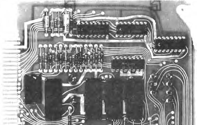
40 OUTPUT CARD PREEMPT CARD CONTROL CARD MEMORY CARD DSPLAY CARD MOTH ER BOARD PROGRAMMER /O BOARD 24V SHUT-OFF.? BOARD POWER SUPPLY SUBASSEMBLY BBON ONNECTORS (4) Figure 2-4. HMC-OOO Controller l Cover Removed to show nterior Elements 2-14
41 Preempt card Output card Power supply subassembly. The cards are interconnected to a mother board by card connectors and the power supply is connected to the mother board with plug-type connectors. Four Ribbon type cables connect the mother board to the programmer/inputoutput board. This board has the programmer connector, input-output connector, and three rotary switches mounted on it and the components for the noise filtering circuits. The interconnect diagram (see Appendix A, drawing number ) shows all interconnection wiring between cards, switches and connectors. The fuse, power on-off switch and mode switch are connected by wire to the programmer/input-output card Display Card (Figure 2-5) The Display card contains the NTERVAL and TME 1 SEC seven-segment readouts; the DAL, OFFSET, CLOCK and STOP TMNG LED's; a portion of the memory address logic; and the interval display logic. Referring to the schematic ( ) in Appendix A: U7, 11 and 14, the time display chips, contain a 4 bit latch, seven-segment decoder, segment drivers, sevensegment LED readout and decimal point circuitry needed to display the time. Data to the time display chips comes from the memory at a CMOS Level (12 volts high), via the DO, D1, D2, D3 inputs. Buffers convert the CMOS level to TTL levels. The strobes, Sl, S2, S3, coming from the memory card are also CMOS and are buffered to the TTL level When data is to be entered into the displays, data is first set up on the data lines and then the appropriate strobe line is pulled low to enter the data into the display's latch. U16 pin 3,. determines if the decimal point is turned on, switch position. times. based on the DSPLAY/PROGRAM The decimal point is turned on only for interval and dwell 2-15
42 ; 2-16
43 U1 and U2 display the interval. The four interval lines, coded as shown in Figure 2-6, are converted to decimal number by U15, a binary adder, and associated logic, U16. NTERVAL BTS NTERVAL DSPLAYED =+ 5 VOLTS, 0 =0 VOLTS <TTL LEVEl) Figure 2-6. nterval Coding The LED displays, CR5 through CR13, are buffered by appropriate buffers. Data selector chips U6, U12 and U 18 form a portion of the memory address logic. When no programmer is connected, U6 selects the interval address to be displayed. When the DSPLAY /PROGRAM switch is in the N1;:ERVAL position, U 12 and U18 select the display address to be the same as the interval. n the other switch positions, the display address is coded by diodes CR1, CR2, CR3, and CR4 and selected by U12. to an appropriate code for CYCLE, DWELL, OFFST 1, OFFSET 2, and OFFSET 3.
44 When a "serial" programmer (such as the HMC P-1000) is connected, the interval is switched by U6 to the programmer address inputs. When the DSPLAY /PROGRAM. switch is in the NTERVAL position the display address becomes the same as the programm.er inputs. When a "parallel" programmer is connected, the display address becomes the same as the programmer address via U18 when the programmer writes data to memory Memory Card (Figure 2-7) The Memory card contains the EAROM memory, memory addressing logic, buffers to and from the memory, the LS chip, restart circuit, and high frequency clock. The LS contains the 60Hz to 10Hz and 1Hz countdown circuit 7 three counter/timers, memory address logic, and multiplex timer logic. Figure 2-8 shows how the memory is addressed for the various types of data stored in EAROM. U4, U11, U12 and logic on the display card addresses the LS chip (U15) inputs 14, 13, 12, 11 and lo. The LS chip then generates a new multiplexed address that is presented to the column memory address inputs A4, A3, A2, A1, A'/J and row select logic input A. The new address has three states, one for each digit, as shown in Figure 2-8. n addition, one row at a time is selected by U14 depending on which dial is selected by card inputs B and C and the state of A. Figure 2-8 indicates that Row 1 (Rl) or Row 2 (R2) is selected for dial 1 depending on the present state of A. R3 or R4 is selected for dial 2, etc. The D input to Ul4 turns on a row only when the memory is being accessed. Transistor buffers between the LS chip and the EAROM convert the open drain LS outputs to the 24 volt level for the EAROM. n addition transistor buffers between the LS chip, U15, and the.ttl decoder, U 14, convert the open drain outputs to TTL logic levels. U14 is capable of driving the Row inputs through a resistive divider network. Note that Figure 2-8 contains a list of the various volt levels at the inputs and outputs to the LS and the address and r.ow inputs to the EAROM. buffered to the CMOS logic levels for use by the display and LS Data from the memory is
45 2-19
46 , O')r-:l o CCJr-:l CDO, LS NPUT. LS OUTPUT MEMORY ADDRESS DATA TYPE DG T NOTES A4 A3 A2 Al AO RO=A a a a NTERVAL 1 LSD 13, 12, 11, 10 SELECTED a MSD AS DESRED NTERVAL 1 a a a a DEFNED BY 1 LSD 11 AND 10 SELECTED AS 1 a a a AND 10 1 a a a MSD 1 X 1 X X a a 1 DWELL 1 LSD 1!< 1 X X a X 1 X X a 1 3 MSD SHOWN BELOW ROW SELECT 1 ACTVE DATA TYPE DAL D C B A=RO ROW PN a a OFFSET 1 1 X X X NONE X a 1 OFFSET 2 a Rl 1 1 a OFFSET 3 a a a 1 R CYCLE 1 a R3 2 a a 1 1 R4 2 LOGC LEVEL DEFNTONS 1 a R5 3 a 1 a 1 LOGC 1 R6 3 LOGC a 1 1 a R VOLTS a VOLTS a R VOLTS a VOLTS x = DON'T CARE MEMORY ADDRESS N ROW PN (READ) ROW PN (WRTE) ROW SELECT <TTL> a VOLTS +12 VOLTS a VOLTS + 5 VOLTS 24 VOLTS 24 VOLTS 24 VOLTS a VOLTS Figure 2-8. HMC-1000 Controller Memory Map
47 A clock formed by V8 pin 11, V9 pin 10, C6, R12, and R13 drives the multiplexer logic in the LS chip. Timing signals TO, and T1, from the chip are used to coordinate memory addressing, and display functions with the multiplexer. According to Figure 2-9, when T1=0 and TO=O, the multiplexer cycle is in the display/program mode. f MAO input is grounded (DSPLAY PROGRAM switch not in OFF position), the LS will generate three strobe outputs, one for each digit, and the address logic will address the memory rows and column to read the data selected by the DSPLAY / PROGRAM switches. When T1=0 and TO=l, the multiplexer cycle is in the load offset time mode. f MAl is not grounded, the multiplexer goes on to the next part of the cycle without loading any counters. f MAl is grounded, the offset counters is loaded with the selected offset time. n the same way the other two counters may be loaded during other parts of the multiplexer cycle. Address logic on the memory card is used to multiplex the address during the various portions of the multiplexer cycle. V13 decodes T1 and TO to four outputs, one for each part of the multiplexer cycle. When T1 and TO are 0, then the 2YO output, pin 9 of V13, is low causing V 12 to select the display address to address the memory via the LS chip. On other parts of the multiplex cycle, V12 selects the output of V11. When T1=1 and TO=O, V13 causes V 11 to select the interval input from the interval counter or the load dwell input for loading dwell times into the interval/dwell timer. On the remaining tw;,o parts of the multiplex cycle V11 selects the offset/cycle address logic. The 14 input to the LS chip is handled separately by individual gates in a similar logical combination manner. Figure 2-10 shows some typical waveforms found on the memory card for the switch positions and other conditions shown. Note that when the display is turned on, the waveform repeats once each multiplexer cycle and an oscilloscope can be triggered on the' display line V13-pin9, or memory card pin 44 (negative going pulse). the scope. The waveform will then be displayed repeatedly on When the display is off or it is desired to look at the waveforms 2-21
48 Tl TO EAROM DATA LOADED TO (FROM) LS FUNCTON LOGC 0 AT THS LS NPUT ACTVATES FUNCTON MEMORY ADDRESS DATA TYPE DAL (ROWS) SELECTED BY 0 0 DSPLAY (PROGRAMMER) STROBE Sl, S2, S3 MAO SELECTED BY DSPLAY/ DSPLAY/ PROGRAMMER SWTCH PROGRAM AND/OR PROGRAMMER SWTCH (J)t\:) o CO COt\:) O 1 OFFSET TME COUNTER LOAD COUNTER MAl SET TO OFFSET SELECTED ACTVE C10 BY OFFSET LOGC DAL SWTCH 1 0 NTERVAL/DWELL LOAD COUNTER MA2 SET TO NTERVAL SELECTED (MAY BE TME COUNTER C20 BY NTERVAL COUNTER OR REMOTE TO DWELL DURNG LOAD DWELL NPUTS)! 1 1 CYCLE TME COUNTER LOAD COUNTER MA3 SET TO CYCLE ADDRESS C30 LOGC 0 = 0 VOLTS LOGC 1 = 12 VOLTS TYPCAL WAVEFORM. NO FUNCTONS ACTVE (MAO =MAl:::: MA2 =MA3 =12 VOLTS =LOGC 1), TO (LS PN 28) Tl (LS PN 27) -, L- 12V OV 12V.- 25 ± 10 MCROSECONDS - OV Figure 2-9. Multiplexer Functions
49 ,. o' 0) t-.:> COt-.:> CO"" CLOCK TO Tl DSPLAY Ql Q3 Sl S2 S3 A Q A4 A3 A2 Al AQ 12Y - 12 =- -...r- 10 ± 5"S Lll ::::l 5Y V V _ 0 12V v- U U U L -U U U " STROBE DGT 1 STROBE DGT v- 0- ::= -U U U SV- t-.-- DAL STROBE DGT _o.+... DAL 2--! S:::::l 0 12V- 12V- 0 12V- 0 12V v V _ 0_ 24V - 0_ 0 24V- 24V- 0 24V V =============L ,U ---JL- U- --DGT DGT DGT n l u:-. CYCLE ADDRESS 1",lg DSPLAY/PROGRAM SWTCHES, DAL 1, CYCLE ACTVE DAL SWTCH, DAL 2 OTHER CONDTONS, OFFSET 1, NTERVAL b L CHP U15 US US U13 U0 U0 U1S U1S U1S U14 U14 U14 U14 Uls Uls Uls US U1S U0 UO U0 U0 U0 PN 29 2B 27 12V o - 12v _ o - o 12V o SV rdgt 1 DGT 2 --r NO STROBES (DSPLAY OFF> u u u DAL 4 DGT 3 -, 12V o SV V o _ :- L _ 12V- o _----1 ULr o 12V - 12V-_= l:-:=:11 U 12 0 V= r- --,u "- ill 1-"'"""'''---lill 111 " DSPLAY/PROGRAM SWTCHES, ACTVE, OFF ACTVE DAL SWTCH: DAL 4 OTHER CONDTONS, OFFSET 3, NTERVAL 8. LOAO DWELL COMMANOEO L TO Tl DSPLAY 20 U U, V - U _ U U U ' 12V, Sl S2 S Figure Example Waveforms on Memory Card
50 for loading the counters, the waveform will occur only once per counter load and therefore it is desirable to have a memory scope and trigger the scope on MAl, MA2, MA3 inputs (negative going pulse) U15 pin 23, 24, 25 or card pin 26, 28, 30 respectively. To make these signals occur more often, program the interval times to be O. 1 sec or program most of the intervals to be 0 seconds. Also program the cycle time short and the offset times to 0 sec. Generate offset sync pulses every 0.3 seconds of greater to make the offset counter load often. For this type of trouble shooting it is advisable to have a storage or memory scopes (2 channels desirable), The clock is derived from the 60 Hz signal. A 60 Hz output from the power supply is buffered by a programmable unijunction transistor, Q10, and an RC network to provide filtering, level detection and hysteresis. The 60 Hz is then counted down to 10Hz and 1Hz by the LS, both of which are available for use by other circuitry. The 60Hz signal is also used to generate a restart signal. f no power is applied to the HMC-1000, U8 pin 4 goes high upon applying 115 Vac for a period determined by C8 and R14. f power fails, the reset pulse will not be initiated until C8 discharges through R14 and R16 enough to go below the U8 threshold. A second input to U8, filtered by C7 and R15, is used as an external restart Control Card (Figure 2-11) The Control card contains the dial select logic, the offset select logic, most of the control logic, and the interval counter. The buffered remote dial inputs from the preempt card are applied to the remote dial priority logic, U16 pin 10, U20-11, U17-10, U17-11, U21-4, and U21-12, to select only one dial when more than one remote input is grounded. U6 is a 4 bit latch whose 'output is the same as the input when the transfer allow bit is low and whose output is the stored dial information when the transfer allow bit is high. U7 selects the active dial when the ACTVE DAL switch is in position's 1 through 4 and 2-24,.


51 " -o +> s:: o U 2-25
52 selects U6 output when the switch is in the REMOTE position. Wires to the display cause the active dial to be displayed. US selects the dial for memory address. When the DSPLAY /PROGRAM switch is in the ACTVE position, US selects the active dial all the time. When the switch is in position's 1 through 4, US selects the display dial when the multiplexer is calling for a display function and the active dial during the rest of the cycle. U2 pin 6 and U2 -S encode the 4 wire, one at a time logic, to a 2 wire binary code (B and C row select lines) for the memory address. The synchronized and offset inputs from the preempt card are applied to the synchronization logic, U10, Ul and Ul1. When a synchronized pulse is generated flip- flops U10 sample the offset 2 and 3 lines and store the present offset condition. U11 decodes the stored offset to a one at a time 3 wire format for use by memory address logic and the offset display. On power up reset, U10 is set to offset 1. The interval counter, U9 (pins 3, 4, 5, 6), is controlled by U11 (pin 12) and associated U16 gates. The counter is reset on power up and whenever an advance signal is generated by the control logic and the last interval input is low. f it is not the last interval, a clock pulse advances the counter one count at a time. U ls-11, prevents the interval counter from advancing if the controller is presently dwelling. Buffers in U5 and U3, convert the CMOS levels at the U9 outputs to TTL levels to drive the TTL gates that require interval information. The control logic outputs the advance interval, load interval timer command, load offset timer command, load cycle timer command and load dwell command. The load interval timer and advance interval command is generated by flip-flop U13-13 based on the advance logic formed by U19, U1S-10, U15-9, is combined by U14-13, and is synchronized to the multiplexer by the counter 2 input. Whenever one of the following conditions occur, a load interval command is generated: 2-26 "
53 1) f single step mode is 0 volts (U19-8) 1A) nterval timer times out (U18-8) at 12V) or 1B) End of dwell (offset timer times out (U18-9 at 12V) 2) f single step mode is 12 volts (U19-8) 2A) Guaranteed manual advance, automatic manual advance and single step advance at OV, (U15-8, U15-1, U15-2 at OV). or 2B) nterval timer times out (U 18-8 at 12V) and guaranteed manual advance bit set (U 19-1 at 12V). or 2C) nterval timer times out (U18-8 at 12V) and single step advance step (U19-12 at 0 volts). Figure 2-12 shows the waveforms that occur each time the interval timer times out. U13 pin 1 generates a load offset time and load background time every time a synchronization pulse is received, providing the background timer C30 has timed out. The two flip- flops, U22, detect whether synchronization is present by sampling for two consecutive cycles. U22-13 is set every time a synchronization pulse is received, and the fact that the synchronization pulse was received causes U22-2 to shift at the end of the dwell interval. f synchronization should fail, the logic directs the HMC-1000 to go to the Free mode. The output at U17 pin 4 determines whether dwell should be timed when the interval counter comes around to the dwell interval. U17-4 is 0 volts, dwell inhibited, if there is no synchronization (U15-5 at 12V), in the Manual or On Line mode (U15-4 at 12V), in the Stop Timing (Man Sync) mode (U15-3 at 14V), in the Free mode (U20-6 at OV), or if the offset timer has timed out in the last 0.5 second (U17-5 at 12V). f any of these conditions do not exist when the dwell interval comes around, U12-1 goes to 12V to command a loading of a dwell time. When a dwell time is loaded, the dwell flip-flop U12-13 is set so that
54 CHP PN +12V U20 1 COUNTER 2-0 U U -12V U13 8 U18 8 C20 COUNTER 0 12V U13 9 f\ f\ NOTE 4 12V 0_ 12V --- NOT E U13 13 LOAD NTERVAL TMER 0_ DSPLAY/PROGRAM SWTCH: OTHER CONDTONS: NOT OFF NTERVAL TME TMES OUT NTERVAL COUNTER ADVANCES. USE 10M, LOW CAPAC TANCE PROBE Figure NOTE 1. THE EDGES SHOWN MAY OCCUR ANY TME BETWEEN THE LMTS SHOWN. Typical Control Card Waveforms, nterval Time Out CHP PN +12 U20 1 COUNTER 2 0_ U18 8 C20-12V- 0-12V U U13 13 LOAD NTERVAL TMER 0_ b 12V U18 1 DWELL NTERVAL 0_ 12V U12 5 ENABLE DWELL 0_ 12V- U12 1 LOAD DWELL 0_ 12V- U12 13 DWELL 0_ DSPLAY/PROGRAM SWTCH: OTHER CONDTONS: NOT OFF U '-----NTERVAL COUNTER ADVANCES NTERVAL TMES OUT, DWELL REQURED (HMC-000 NOT N SYNC). Figure Typical Control Card Waveforms, Dwell Started 1' "
55 U is 12V. U12 is reset when the dwell time ends, or if the offset timer times out during dwell. Figure 2-13 shows the typical waveform when a dwell time is loaded into the interval counter. The other half of counter U9 (output pin 13) is used to generate a 0.5 second output every time the offset timer times out. When C 10 goes to 12V the output of U 17 goes to 12V for 0.5 second, preventing dwell, should the dwell interval be started during the 0.5 second window. This circuit is included to allow for "jitter" in the synchronization pulse if the master controller is electromechanical Preempt Card (Figure 2-14) The Preempt card contains the buffers for all inputs and the control logic for the manual advance and on line modes. The buffers, made of CMOS non inverting buffers, are used to provide level shifting from 24 volts to 12 volt levels. A pull up resistor pulls the inputs up to 24 volts until an external switch grounds the point. A resistor divider brings the voltage level at the CMOS gate inputs to 12 volts. A capacitor between the input and output of the CMOS buffers provide noise filtering and AC hysteresis. Note that a synchronization pulse is generated every time an offset input is grounded. The preempt board generates a stop timing command (U5 pin 6 at 12V) whenev.er one of the following conditions are true: Manual synchronization is grounded The stop time input is grounded The on line input or the manual input is grounded and both of the guaranted interval inputs are at 0 volts. 2-29

56 " ;.;: 2-30
57 A single step mode command is generated (U6-4 at 12V) when the on line or manual advance input is grounded. When either the manual advance or on line input are grounded, the single step advance is enabled. The flip flop, V1, stores the fact that an advance was commanded even though a advance has not yet occurred. This happens when an advance command is generated before a guaranteed interval has timed out. The flip flop, U1, clock input is controlled by select logic U4-6, U4-9 and U7-3. When the on line input is grounded, grounding the advance input causes the clock input to go high. When the manual input is grounded, grounding the manual advance input causes the clock input to go high. When both on line and manual advance are grounded, only the manual advance input causes the clock input to go high. Note that the flip flop is reset every time the interval counter is advanced or power up is reset Output Card (Figure 2-15) The output card contains PROMs and buffers for all outputs. Each PROM chip is organized as 32 eight bit words. The 32 words are addressed one at a time by a 5 wire binary code. Four of the wires are connected to the interval counter and one wire is connected to the 1Hz clock. When the 1Hz clock is high, one 8 bit word is addressed relating to the interval being addressed. When the 1Hz clock is low, another 8 bit word is addressed. For each interved there are two words programmed. f a bit in the word is programmed as a logic 0 or a logic 1 for both words, the output state for that bit will be a steady off or on, respectively. f a bit is programmed logic 0 in one word and logic 1 in the other word, the output will turn on and off at the 1Hz clock rate causing the flashing state. 2-31
58 2-32..
59 " For example. if for interval 5 (binary address 0100) the words are.programmed as follows: thz CLOCK EGHT BT WORD High Low MSB LSB all of the outputs will be steady on or off except the most significant bit (MSB). which will flash. The HPP-1000 Programmer automatically programs PROMs for the selected state (On. Off. Flash). There are five PROMs so that the output card can accommodate 40 circuits. All of the circuits are buffered with open collector high voltage inventors capable of driving load relays or other circuitry. Note that 32 signal light outputs are pulled up tp 24 volts with a pull up resistor and the 8 control outputs are pulled up to 12 volts. The output card contains an auxiliary flashing bus circuit that supplies a 24 volt square wave at the 1Hz clock rate High Current Output Card -- The High Current Output card performs the same function as the Output card except that the output current sink capability is increased. This card operates in the same manner as the card described in paragraph except that no pull up resistors are included. Note that when using the High Current Output card the 24 VDC supply limitations must be observed. The 32 outputs available at the connector are the only outputs modified by plugging the High Current Output card into the HMC-1000 instead of the normal Output card. Unless otherwise specified. the HMC-1000 Controller is supplied with the regulav, Output card. 2-33
60 2.2.7 Power Supply The Power Supply supplies all power to the HMC-1000 electronic circuitry, 24 volts for cabinet functions (including load relay drive) and 11 volts dc unregulated to the HMCP-1000 Programmer. Two transformers step the 115-volt ac 60 Hz down to lower voltage levels. Both transformer outputs are rectified and filtered by a capacitor input filter. (Before rectifying and filtering 30Vac p-p is supplied to the controllers restart and clock circuits.) These filtered voltages are regulated by three terminal integrated circuit regulators into 5 volts dc for the display card, memory address logic, dial select logic, and output board; 24 volts dc for the EAROM, and the input/ output circuits; and 12 volts dc for the CMOS control logic functions. The filter capacitors are sized to store considerable energy. When 60 Hz power fails, the capacitors can supply enough energy to allow the power supply voltages to remain regulated for some time after power loss. The 24 vdc stays regulated for at least 1.5 seconds after power loss while the 12 vdc stays regulated for at least 3 seconds after loss. Both times depend on the external load on the 24 volt supply. The 5 volt supply remain regulated for at least 75 milliseconds after power loss. The interval counter and timers ar.:e supplied by the 12 volt power supply, so for momentory power loss of less than 1 second duration, interval and timing functions continue. When power returns the power up reset circuit will restart the controller in nterval 1 if the power failure was at least 0.75 ± 0.25 second long. 2-34
61 A 24-volt shutoff circuit turns on the 24 volts dc to the memory, the, input/ output circuitry, and the external cabinet fun ctions, when either 60 Hz power is present for at least 50 milliseconds or the restart signal is low. The 24-volt shutoff circuit turns off the 24 volts dc when power has been interrupted for O. 75 ±.25 seco:ld and the controller is being restarted in interval 1. f a controller power failure occurs, the 24-volts the controller supplies to the cabinet functions will also be interrupted. This causes the cabinet's voltage monitor to switch the intersection to nashing operation. This occurs within one second of power failure. 2-35
62 SCHEMATCS, APPENDX A ASSEMBLY DRAWNGS AND PARTS LSTS A-l
 54 -o \"/1 J ;n';: 1[l}i-t :;:Y't====rm -;! ll.?:!'. Ftv.t\RAR. -_. e:5-1 :-..'J.\ E.")
B -,,)1:,\" e,r/lo,c.l..e.t, CON... 2023Z74-047 AP,2000U,t\", SV i:?f--rt:;lh!t\" T(.")
 _SRF-O ( t; '\ &- CQ.")
}( AS SHOWAJ. 4 PLACe:... $ -Foe BUR4J-N.C\"'otTuRe see L.l::'l1wn'-t 28\",',(;;-(.}. 2 -Foe TE r rl>tture ':,.")
 5.,5123-1=- - ;:QXii.;L - l_ J(::: Z'3C!.t::.!t.:4. _ U.!:Mqk....i:!:(CfP/-j{...1.D...PLA,V } c{f1} '-..;;;:.")
63 S-:l..V -002 L : ; _ ",-fer \'!J 01 CO CO fl Jl 1l '1l 115'0 j -)F '4),::) ", ::Af-'LE E'JUTJ-::' 1.JAr;2'/iM c..ale; /':"'/E 11"" // ; ).\1 [.:\_. /../.. TEM FWM /3 { K'E.P) Pl...!---l -"r.i-":. v _ PoLl: _ -.J ''U' F (A-/'"". f ',5 ----rue" -J RrM.'T (+- toljt.at\cne.j.'t-o ".'"'. C,",,M &.5:... (rwe) 54 -o "/1 J ;n';: 1[l}i-t :;:Y't====rm -;! ll.?:!'. Ftv.t\RAR. -_. e:5-1 :-..'J.\ E."-l['\,.A. 834.SS - F:JA,!"l.,:...';;.;. E34"5S-Z LAP.T'N 2. _ 11.5"5_14::OQ.. ell,,!. q.m-?, 2..Q. DA AP :::: S-71 "',)LOER /lj<>o/sno3 <> M':' ":.!-::;t- -4..' WA5ER, HELl -S-'<Nl3 J 1: Ol41DUsr COliER 'l".l ; ' Z80Z2.2SS-00ci. CAPou;-7'4ov,cc- 260ll':,)B -,,)1:," e,r/lo,c.l..e.t, CON Z AP,2000U,t", SV i:?f--rt:;lh!t" T(.,C:T e4'5 -z <48, SPR/illGUE 4 4 A1S i - str V(:>.Pft.-..:.:._ , 18 ":!...s!..:-sf A';;t{.fJ_!!!rE.c.!!:! 5 5 M v"''''/'61<:. V... r' 'r" 1.0, 10 M5.J.5O,,:z. ':'f'.f W.?;l.f.: -. '-''''' LG. c, 2 MJ5i'2"6 '-C...'eW,""M '9-?:Z..r % Li'. -:- i?:, Msis.:c";; ::."6 SE'E'w. ", M 4-"h 7/... L " M.='"" i,.,-"",.,-- -,",.., 2 ",,,,_,... Nur B34.r:.-3,../...'-!-Sw1rc:H) _SRF-O ( t; '\ &- CQ..047 OAP. ) A::'SY (Tt:M /3) WtH RJ/'vll:.J \L 'UEF (TOrl 27) BOTH SO.!:.s AN ) Ae":UNP e,decn CC/.,/NLCn:;..e.s AFTER SCXDE!!JNG TC b'c:-1ro "'SY (!rcm 6). NCC:11711'/f. ( CA.!1LES. N :;,wlrr;rles O CO,/N C7'VRS. -(.:emea./t,-n eaj::::/&c. MN 4PL4LC'. -: - LOCATE APpQ()}( AS SHOWAJ. 4 PLACe:... $ -Foe BUR4J-N.C"'otTuRe see L.l::'l1wn'-t 28",',(;;-(.}. 2 -Foe TE r rl>tture ':,.EE L-RAWn".:.B(,Zlj-;.-r, {:'('e,-e/,..j E E Di?/\'WA.tJ Z8o"'1()43. - ':01:1 SYSTEM NTERC0A.1NE':T DAGRAM SEE: RAW..., j:', 49' \ 3n' <.,,'...: 1-',::,-.11,',/-.h-R... lda ::;....'-,:-.:: :".;,: "'/....:..-- -",. '.N_ -_-.f...., :- ",,:.. '\ 4 '/,.,,40_,;";,_,,- <17 t t.,... '1M) 5.,5123-1=- - ;:QXii.;L - l_ J(::: Z'3C!.t::.!t.:4. _ U.!:Mqk....i:!:(CfP/-j{...1.D...PLA,V } c{f1} '-..;;;:._"._=--::@...L!.3J2.! _ 'i:l*(.z'(.79' 5 F-WK. vf.-fl.y AS:;) - -'U-:;z..":'':1 rp''s:.f.(,r'2. +-;._:. :;.;: ( f;pf/"as./s fir :t +U,;- p.
64 ,--., :J> 0, COt.) CO PART NO.. B ,.. J3-1 '. '".----:;,.J(,-7 -OO._ j>J{,- '2. UN(2.te -004 DC -OOS J L REVSONS ZONE LTR DEscPtlnlOH DATE APPROVED tk bl'j LJ R /;...J6-5VOC CRt-d.?. wt t:, 5 uf' DSFV.y T: \/1/4001 -r f"' 50V \6 CR VDc:. '.B1.J U2, kj- S <; VDc 4J>RE1 Cz. C"'f f- To'U CR" 20000Mt Jel Tv 50" '" J ---'>.J'-3. BLK --- BLK bo 1-11:. BLU 6RN RED '24VPC. 9N ORN GoRN J' 9 7'm.CP KEY" ;>J'- (, 5 Go 7 15 GRY BLU 12 WHT 13 JS- \ Kcf r--- q - 8 ' (P C-Cy:; ' VO T2. Z-5-Z 10 U3 H-vDe 1-0 J.4-1 C.R5, CR4-' HT '- 2 + BLK PWB -to c,4 - REC 2.4V P'O'" 0.1 UF SQl."'QA ORN SHUTOFF "!OO VDC 16JC".uf J- l C5 CR7 CR'- 4.JV '?> J.G-6,'- VDC GRN 2.0 ' --'>..)(,-11) J EJ6-i1 -,>JH _ c-cl "'RN J.- 1'- GNO... J(,-'3 1DOUTPUT : COMMON QTY PARTCR 1824 NPUT "'--i. - 'TvR REMARKS ':;' REQD DENTFYNG NO. GOVERNMENT AND AERONAUTCAL,.DDUCTlO TOLERANCES UNLESS/' O"AFT'$MAH M.KOLA (, NOTED OTHERWSE HONEYWELL DVStON OECKlEft -J\.030 red.. OEVENGfl, " (.-..:,-!,.xx.x ± GLES EHQlGMGT.04-:' l MA.xxx ± +2" 1 CONTRACT l HMC.1000C NO. NC. P "NN=:=:1J POWER SUPPLY ASSY SZE CODE DENT NO. DftAW1NG NO. UNLESS OTHERWSE SPE:C,F"ED', l ,8 HMC 1000 C RE'5'S'TCRS: '/4W 570 l NEXT ASSY USEOOH REFERENCE Al'f'LCATOH 1J1'NSH-SEE NOTE "- SCALE NONE _ET, OFl
65 EARTNO' ZONE LTR REVSONS OESCRlnlON DATE APPROVED. /! '" '. C3 REF- '2 T2 31 J -J, 01 CDH:>. CD o ORED T2. o 0 _CRS CR4 _CR 08"" CR7 t4-aod -C2... O"'T O.ro C' B"" MOV 4.701:.02.&.2S±.O & VEW A-A (TYP OF" 2.) /.100 DA f.()le OR.053 CA Pl.ATED "'HRU HOLE REF. &- SLK-SCREEN OR RUBBER. SJ1.MP APPRDPR\A,E D"'S NO. AND REV LETTER. NB. Po.":>c;',(. z..9o!.ol & & ZNC PLATNG QPTONAL ON ALL MS HDWE. &-ASSEMBLED PRNTED WRNG BOARD SZE PER NDCATE.D DMENSONS, y REOD DESCRPTON REMARKS NO. GOVERNMENT AND AERONAUTCAL ",OOUCTS DVSON 2CX RDGWAY """KWAY MNNEAPOLS. MNNESOTA 114'3 2..-FOR TEST FHURE SE.E DRAWNG \OZ. -WORKMANSHP STDS PER es8196-0/, -'-'----'-t' SECT G M. REFERENCE NEXT ASSY USED ON APPLCATON -SEE NOTE TRACTNa. SZE c POWER SUPPLY AS5V SHEET
66 " Honeywen SUPERSEDES S '..' REV. DATE E.O. REV. DATE E.O. ENGNEERNG PARTS LST POl.0E.e supl'f AS'S,!. TYPED BY PPRD. BY CHKO.BY DATE PRNTED N U. s. A. '2.sou>(.'79 SHEETS SHEET NO.'.'3 '30..- lit 0 C( 8 TEM PART NO. PART NAME \ NO ' R Sianal 1 Tl 1 ' -uu TRANSFORMER Signal 1 T Go-005 U1209K REGULATOR Fairchild 2 Ul U2 Z C7824CP REGULATOR lotoro1a 1 U3, r 1C7812CP REGULATOR Motorola 1lu4 } N4001 DODE 6 CRl, 4,1},7 ( uf 35v T Sprague ll}()nl f/u'j llff 1 r?.17 7 i;'{"!-ot/.;1" f TOR Z c.5.t. 2. R uf 50v ll}()nl./u'a C,, 1 C4 46, S / PJ\J HD 1 1ACH SCREl4 2 ' THEPOCOTE STOCK NO. 249 SLCONE GREASE ny 1? , P.S. CABLE (15 PN) 1 13 ' '-002 P..S.c"A6LE (15 PN) - 14 ' ' PW6 ASS, Z4V -, 15 HUTOFF S HEX NUT, SNALL V150LA1OA 10V GE flountng KT 4304 TO-3 CASE ThermaloY 2 Z HUUSEAL 1 GAL PER (50 UNTS) AR AR 22 M -M q A-5
ECTOR -:.")

W RE 22 AWG \"'-T An AR 1f> 28020'3 \as- '72. LEADWRE 22 AG RED AR All:. 37 223'BS -,qb LEAD.WRE 22 AG BLU AR AR 38 2.")
67 Honeywen PRNTED N U. S. A. SUPERSEDES S '" TYPED BY PPRO. ENGNEERNG PARTS LST REV. DATE E.O. REV. DATE E.O. P Ov.:>ev- SU"p., As,=>'(. 2BC2DCo19 BY CHKD.BV1DATE SHEETS SHEET NO. ""3. '36/ lit PART NO. PART NAME ' COt..\l<.)ECTOR -:.ET), Elec.T P.W.B. Arno 1?l; AAP-52 POP RVET CHERRY 4 28 /K// 'u/-u 6.00 Ui. X. JU U TY-272 M Wire tie T&B QOl P.O. Board, Power Supply 1 t OO Transformer Bracket 1 t 32 ; -/:su. B08853AOOl MCA MOTOROJ A? '2. '1'1 B51547F015 BUSHNG r l0torola 2 '2 34 -B03 B52200FOQ5 C(»tf. 1OTOROLA 2 ' cooa. 3 le5 ='79CJ LE()W RE 22 AWG "'-T An AR 1f> 28020'3 \as- '72. LEADWRE 22 AG RED AR All: 'BS -,qb LEAD.WRE 22 AG BLU AR AR ''2.b''-52.9 CS CAPAC.\TDR 0.1 UF 4OVC. 4 26?Q 3Co}. " A-6


68 PART NO / REVSONS OESCR'TOH DATE APPROVED,N"H:,.""Vl PMoU.', r- R' K l J "> "' V,... <: =i? Z l :: 7 b.- J,... q ty, :J> 0. CO...:J CO," 11, i / L\JtQ.l:ST ''is C'5" vg cr. 13 NOT u 'O ca L(SD P""T"OR DENTFYNG NO. A :: 13 n\i!634 5n 0'(1"_1" 32 5i "T 4' 2 t- ""1 -_... r>-:' - )c,. /.(. OOVERWEHT NJ AERONAUTCAL DVSON.. RDGWAY '...MAY.NNfNOU...-sorA NO. PRlNT O CRCUT B041W REFERENCE 280,0878 -MC-OQ(j.-xr,..-r USED C* Nft.lCATtoH MATERAL FJNH-sEE NOTE CONTRACT NO. _zs c ASSGWBLY, DSPLAY DRAWNG NO n 10.3
69 PARTg...- j-& REVSONS ZONE LTR DESCRPTON DATE APPROVED 0 B, \m,ce" 5 08 Cl Cl CR 0 --( 2LJ- ---@=:J-- " :J> 0, CO 00 CO ", J J G, 0 - t 0, <;'1 f- U/4- -c&lj- CR ---{ [J- ---c:slj-- ---j cos r-- - f U 1,/7 Cl B[J E] E] E1 B rj [J B, --au @fj-? U uz \ 0 0 BOTt 1 SDES &. i &-CC'T 5'DE " "Me" m. cco', "'- CONTNUED... CR (H:M 13) NDCATES CATOOE, SHORT LEADWRE.. 4-WORKMAN51-1P 5705 P R. E ;.. SECT G$M'\-.& Nc,TE. CONT\JuEO; COAT BOTH SDES OF P.w'B. WTH aty PART 0;:1 NUMtr«;LA URe OR HUMSEAL. DO NOT APPLY COATNG N "EMARKS REOD DENTFYNG NO. DESCRPTON f::,'" AREAS NDiCATED OR TO DSPLAYS U U2 U7 TOLERANCES UNLESS DftA"""AH HONEYWELL GOVERNMENT AND':,:'AUT'CAL..OOUCTS U AND U4 OR TO CRS _ CR3 ) J, NOTED OTHERWSE CHE.CKEft NCa :zeoo RDGWAY 'ARKWAY MNNEAPOLS, MNNESOTA DEl/ENGA.X + ffi- lo" FORMED RUBBER STAMP OR SLKSCREEN.XX ANGLES! NQftOMGT APPROPRATE DASH NO. AND REV LETTER.xxx + +2".,. PeiNTED CleCC/lT BOARO - FDC TE5T FlXTUe see DRA WNG J MATERAL CONTRACT NO. ASS&'v1L5'iy:, OSPLAY FO,e PROCcj:)t/, " SE.o,eAWNG 2802/038 ) ;;; 1";;20681 NEXT ASSY USED ON REFERENCE APPLCATON FNSH-SEE NOTE SCALE z.)(. SHEET 2 -

 4,t!")
 (;EN lnst. 2 Ck12 13 '7 28022272-269 402ES050AD104f\" O.")
 6100 CARD EXTRACTOR S;1.r ;; t1s 16562-209 ES-094 ROll P\"S 2 23 28020680-002. P.C. BD, DSPLAY 1 '2.4 182-001 la27 CONFORMAL COATNG HUmSEAl!. AR '25,.")
70 Honeywell ---- MCROCONTROLLER REV. E.O. REV. DATE...VE.O. rncd TYPb BV PPRD. BV C 6/29/76 v- SUPERSEDES PER5"D"U". ENGNEERNG PARTS LST CHKD.BV PRNTED N U. S. A. 2.80"2..0<08\ -00 DATE SHEETS SHEET NO. :=><... r i-"'"... PART NO. PART NAME ONTY USf T&\ :99000b TL C. Tl...' NS TR' 1!J 1 1 -UU UG8 1. C. 4 U H C04009 C RCA 2 i < L C C. -, U SN7400 C Sian 1 l': SN7402. U' 7 E,...J r r- SN7404 l. ". ') R q ' f SN7407 L v " 1!! ; '" SN7406 'f 1 '1,. i SN7483.-, 1 '11 r- ' r (' " SN74157,, l... if. 1/ i R rl91 4 oy' 1H 14Q DOD. 11 r. R 1 / ') 4,t! LED DALE., Rl;_- R ,.. ' v r, %.'.." RESSTOR 14 :R 1? l; q l!l / 1 1/11 / t; n.. i i 4\-1 5% C. C. RES:;TOR q RR- R116 ts RESSrOR R MV50154 L F:,) (;EN lnst. 2 Ck12 13 ' ES050AD104f" O. 1 u f SOv CAPACTOR 2 C v SPRAGUE k-l50d685x9035b2 _--6..,.!Luf_.:APACTO 1 C PRAGUE 150Dl05X9035A? : Ouf.v r'apl\rttor 1 -t;, _.. _- f ':fqt - NATURAL COU) 6100 CARD EXTRACTOR S;1.r ;; t1s ES-094 ROll P"S P.C. BD, DSPLAY 1 ' la27 CONFORMAL COATNG HUmSEAl!. AR '25,.- HE S-571 SOLDER SN60/63 An " '6 " l' A-9
SPt... \"'.q4 c-tug5' +.:$ 3 ft 03 \"/u ' t 03> \", 0). 0... COo CO lart:t.l.';:,. il..k p,lu\"4 =- ' 'P'''j:.ot 4,,)b. ol 1\"1 Ekz, C!V91 O\"... otl< 21-..l: :r-\"\"u», H/- -!Lt. T a...\" tel: Co.")
71 PART NO. Z8020G83-00lj flow Sl:"% -Row 4-S"oc. "tbb,g" 4,.'#3. "..., + D LA,a :, 3 ts., C.4 u> 0<-=2 '>,71; c«sl;t 3,7,7& oj. 1'11. +Zt J> '7,.CD, 3 '>< 02. r/u 39 O,?"".t 49 _ '9') (.. A 3'. --.=1'.,, f# A J')SPt... "'.q4 c-tug5' +.:$ 3 ft 03 "/u ' t 03> ", 0) COo CO lart:t.l.';:,. il..k p,lu"4 =- ' 'P'''j:.ot 4,,)b. ol 1"1 Ekz, C!V91 O"... otl< 21-..l: :r-""u», H/- -!Lt. T a..." tel: Co....""QC: 280zoe" , NtUl:ATlClll -.oclll t,.,.)'c. ---,"1-9 J'"... 9.lJy. S363 "'-""61 0 Yl "., 4,. c.o - -u ''" < Z4 '7 'PP< 'Fi;l z. ',."".. " l"'ll r.. ' J1 r 0i _ -:J::..,.q 17-._ '9., _ ' ClH.'(O..A '4-11-'" - 2Q.7b L..UST '1171 l{ <ll() V. JO v -- aavo_...,... 3 )-&> 'i \L...DQlMY PARKWAY A"" PCB ASSY-MEUORY _...
72 PART NO. ZONE LTR REVSONS DESCRPTON DATE """OVED o 0 o' CO... co... ". ErG ElG -±j cz r- '6 '6 '0 <&- e7'o,e/.3 tit c.elo -'E?/O e9.e7 8 -[ D- '8 '8 B--1E:} [QJ OQ4 (]J:J B\ r-"'- illl\ll\l QZ Gl7 Q.S D Da3 DDQ DD<D 1e3,e40 '8 UO -[ 0--- Q Gl8.e"'10 e. es7.e.:.3 e71 o <l?og WORKMANSHP ST05 P R E , G? M. PART OR DENTFYNG NO. ftemarks GOVERNMENT AND AEROf\AUTCAL Pft' VSK)N 2DD RDGWAY PA'U(WAY...ENOLS. MNNESOTA a. ALTERNATE.: MC14093BCP rx r'\./+r.-- roo... 9 P,eNTED elect/t BOARD / -FOR. TEST FXTVteESee W/NG( MATERAL CONTRACT NO. A.5SE"MBLY, MeMORY" FOC. PR.OO Dtllee Sec OR.4W/NS ftefeftence NEXT ASSY USED ON ""PtlCATON SH-SEE NOTE SZE c SCALE - ET
73 Honeywell PRNTED N U. S. A. SUPERSEDES ENGNEERNG PARTS LST 'ts....-"" MCROCONTROLLER 2.802OG.B3 REV. E.O. REV. DATE E.O. Ml:llnDY -OO C 6/29/76 ""-ft,t.1ll TYPED BV PPRD. BY CHKD. BY DATE SHEETS SHEET 3 NO. < ' TE'tJ -... PART NO. PART NAME No. YYUUUb NCR05 C NCR UO SN7400 -UU C Sign 2 U3,4 2- SN C U5 3 SN C U!l/U.UlJUlJ SN7407 C U2 99QG.G17(1-(101 SN7445 C YYUUU SN74155 C un YYUUU/ U4., N74157 C 2 Ull, n.uuujaf?""ool C RCA U9 YY.OO C RCA u BE C / RCA u UO C RCA u6 2.B02.0SO-OO C (Mor)otJwl.l. $SC,o,Ail2tOO20 U5 ( arg scale int ire) K RES,- k w 5% CC 13 R6.8.c i i ; K RES k,\\1 5% CC 8.R1i7 t ru 64 S RES, w, 5%, CC 47 K <0 R5 18 Rn RES, w, 5%, CC 1,>.6K q Rll 2 41 t ru 47 t l -4 10K RES.!o w 5% CC 31 R Hi lq thru _ K R.':.!.o w. 5%. CC " " look RS. k tj 5% CC R ,>10K RES!..: '( 5% CC 1 R'i'i UF 35 V 1'i00O'ixQ03'iA2 tant cild SDr C'i UF 35 V 15(0685)( tant cap Spr 2 C1, UF 50v 402ES50A0104M cad 3 C3 4 c 24 QQ-S-571 SOLDER SN60/63... AR 2.5 Hf,lQ1 l'.) CONFORMAL COATNG 'f AR A ,q


74 en Honeyw PRNTED N U. S. A. SUPERSEDES ENGNEERNG PARTS LST BY... MCROCONTROLLER 2.80'2.0(.83 REV. E.O. REV. DATE--"""'E.D. MEMORY - 00"2-6/2q/76 TYPED BY, PPRD. BY CHKD.BY DATE SHEETS SHEET C NO. e: 3 3b "":... ""- TEM --"' NO. PART NO. PART NAME v 402E050AD391K cap c N3904 transistor, NPN 9 Q thr u m6027 transistor, QO Nq14 nr ln414r diode CR tl ru pin C?nlU"e.?h_l rr"" T.r, 1 11n pin C ir20wff,40-1 rr"" T.rln" ; UF 20 V DC lc;noln6xq020b2 r"n C::;n..? nat color card,] nn C::;,,'"? "?>O 3\ f-' nr 34, -001 Pr.R Vle...f\rv 1.,. 3b 1S ( :'-2-s()q4 roll nins ",.. A-13
75 > o' col-' co PART NO. 2POlO(,8S,ool -m ' {ED- " /S 0, REVSONS L ZONE LTR. DESCRPTON DATE _ 1!',,", L..J L.J =BB=.e7 'R '8 't3 'B 'B '0 +1 C7 --c:: Z:::J- '8 1 r-v- - "" (O \e300 ZJ T3 'EJ 'EJ E [J JtlB' 'EJ 'EJ TJ 'B '8 -T }- -cm:::j- +1 CGo '\ 4 - WOR.,KMANSHP STD5 P R 1: ) ($ t M. RUBBER STP-MP OR 51L<SCREEN APPROPRATE ASSY DASH NUM3E:R AND REV LETTR PART OR R DENTFYNG NO. 2- FOR. T ST FXTURe Sec O,e.qWNG FOR. "'" TOLERANCES UNLESS / p,eoc{;ouec SEE D.e4iVlM> NOTED OTHERWSE CHECKER NO';,;' DR REMARKS ':.:. O,.Af'lWAH f7/7. /h"s l: sene-matc OAG-eAM ON SHeET.3.x EO OEVlNGft. /).,L:"..,,lAS.';', LES.xx f FO- ";UMP OPTON.xxx ± +7!'.,. cl MATERAL Z802.\l\,,\q HMC OODe HMCOOO J NEXT ASSY USED ON "EFERENCE APPLCATON SH-SEE NOTE / " NGRGMGT CONTRACT NO. GOVERNMENT HONEYWELL NC. AND AERONAUTCAL "'OOUCTS DVSON MNN=':::N:A13 PRNTED C,eCUT BOARD ;'; O8-;0685 ASSEMBLY., CONTROL SCALE z.", j""eet of':3


76 Honeywell SUPERSEDES -_...-ro-._-,-d ---r_..- -,-..,..-O::::'----l MC RO CO NTRO LL ER REV. E.O. REV. DAT:.., E.O. CONTROL PCB C6?1/229L/.!...76+!/iq,!()n,.ul+-::::""-_---i ':>1< ENGNEERNG PARTS LST 1 TYPED BY PPRD. BY CHKD. BY DATE PRNTED N U. S. A. 280'lOb8S -005 SHEETS SHEET NO. 2.l:L b t ::::...o;;::----l PART NO. PART NAME DNTY USF SN C. SGN 1 U1 SN7400. C. 1 U2-991) SN7404. C. 1 U C C. RCA 2 U C04042 C 1 Fi SN C. SGN? tjl R '::001 C C. RCA 1 Q C04013.C 5 u ': C04002 C C04025 C 1 U1 5 / C04023.C. 1 U16 / C04001.C. 3 U '- / C04011.C. 1 U C04049.e. 1 U21 /',J T K 1/4W. 5% RESSTOR 10 Rl-RlO ", K 1/4W. 5%. RESSTOR 3 R /" look 1/4W. 5% RESSTOR 3 R /7 2802? OOluf 50y CAPACTOR 2 C3,l L:>O::<::! nn 19Onf\ARlC Q03B uf -",-3..:...5v-,-----,C:..c..A..:...P...-.-:;.S,,-P.:...;.R:..;...AG.::...U::..;E::...r-=2,----;=-C.::...6,L.7=--t--t t---+--t--'/-''----;1 402ES050A0104M.1uf 50v CAP 2 14' E050A0471K 4700f 50y CAP K 1 /4w 5% RE S 1 R13 '2./ & PC Bd.. Control NATURAL COLOR 6100 Card Extractor SAE MS c.'2. -'Z.7"5..o4 OLL PNS 2? 7-4 A-5
77 Honeywell PRNTED N U. S. A. SUPERSEDES ENGNEERNG PARTS LST '... M \e.. Oc. OT ROLLE 280'2.0BS REV. DATE E.O. REV. DATE E.O. c...o",5t\<'ol Pc. -OOS- TYPED BY PPRD. BY CHKD.BY DATE -Oos PART NO. PART NAME QTY use SHEETS SHEET NO. 3 "2.b r.es., CC, look,!,m,!:i% 1 R19 7-(, t:'nj1)f NO CAP., CER, 0.1 uf 50v, 20% 1 C8 402Ep050J\D 041 (mcon) Z7 00-S-571 SOLDER SN60/63 AR V 11\27 (HUMSEAL) CONFORtL COATNG AR z..., \"750Sl-00qZt AW6,BARE.C;OL\t>W'Q.E AR (JM?R\ - E2.) 30 QqO004'7-oq'2..OK")/4W,SRES R,a 3/. " ". A- 16
78 :J> 0 1 CO... co'-:j r c '"<t O'Jt\L " \J l- e. \J> Ot"'L., W 0< "- s: D,L...)ff$Eil "'NC OfF'S'"' '3 e,::'-',/'-f( OPP5 10 Pi><> L" N.(q/lL U-f) l'h'k:() 42. '> j r" ')cr.-'r----,'t j j 4 >- u_.. _ v $\AJ''''(to' - A<..T...t.. /1. /3 40,i <>, ''J -t'" 47 /1. _ R'? /l<43 D5PL...'1 81'-1< J, L- 'JZ- 2,.' S r " 2l\ 3Po f 4-.+ ',,_ 'Rl W"' )! ;'.';' J.! (0 «J.'!ll ) J ---( 1' VOe )., L"rJg n: W ;. '1 21 " m= "1 1' '98 C>' J11e t Q \) "'l. D. --"'<.<; ', J +'2v 4'1...f.j',4 ""'" v C+. i.,i! 'M5'b CS'., 9 "'::' i C06' C. C), 1,., =====L:>79 l- )! T 4-4 ) n t --: "Uf l 4'6> S' Vh /01! "1 -, '> " u 4_. /,/7 u.. ---! -r--,v _ /" f 7.VS-r;; 94 >1'14'" 'fl L. j' '( _ -4/" '> r '1.1 H(,,,,1(.-:" 1J...i'O U R' c, "(.L" ',-TC;P lv-"f. "4-:»---,,,o.-:,J! ' '0'..-N\J... t\'\. ";l/o ":N: a' t:f==.el=::- JGi-: \..0"'0 OwE:u. 4-1,( (,'lap,..n<f"l U) v >-! 'e., _ c<:, T r '1 ;::;'. )0 /f-e'i:r 'H1(fl.'L ""." """"'" " ' ' (..O.)Ni(R '2 c;')' lot <:.-,- R D,.,CSL.L. '/o,ft.;,qv"l '2.2 30K ' '-:'MY,. p NO povlcr --L-<' 37 _. o lu '402 14'-1'7 A i <}' ') u ,4- - '. 1 U4)Ll 400 "e. a.k. '104'l. - 1(, '0 Ll?, ull "0/1, i. - 8 v' 4-<; l, U O,",Z, ,4 '.., V'4- J 400' , 1)1, 40v, -\ 14., Vi. 402; - 14 ') un,vb,v' 400' - 141L V'l ;4., _ \)11 404Q - 't 6..,0 CW('j oe, (l.o.. " orc;c-7\...,ts ('-..up-) ""<lo',,", <... LO:;: t: ND<.rnJt. lpps (C"OS) clo'corfs«,.,1m(fi \ l> fls-...".c:. C"'-J3ruiJPl JJ pelnted CiRCUT OAR.O ---- A5EMBLY, c..omol.. R.!. "9 NN 7G _VS ON J'M,C-.--:'O':'.9.._ :t',_ :-:l' ----l '-111.'/.,. AS5Y 280ZD8'1 r. 3 or-3 H-ONEYWELLlBlC lzs6 RG.» t J
79 Honeywell PRNTED N U. S. A. SUPERSEDES ENGNEE'''NG PARTS LST ". MCROCONTROLLER '2.80'2.0<087 REV. E.D. REV. DATE.-'...E.O. PREEMPT BOARD ASSY. - co,,?- c b/29/76 W TYPED BV BY CHKD. BY Pf'RD. DATE SHEETS SHEET NO. r:::: 3 /..,., ', TEM PART NO. PART NAME ONlY USE NO l-001 C C. RCA 1 Ul \ C C. 2 U2.3 ' C C. 1 U4 ' C04023.C C C C04001 C 1 U7 to K 1/4W. gx RESSTOR 12 R1- R11. R 5 ; look 1/4W. l).' RESSTOR 23 R ES50A0104M 0 luf 50v CAP 1 C3 q '''75'=> SO\)b85X03 S82.. b..8uf.35sv.cap 2 C /-0' uf 200v CAP CERMAC 1 C4 '2882l,l. C."-C'2.9 SPRAGUE 225P22491X uf 100v 'cad 11 C5-C15 1' NATURAL COLOR 6100 CARO EXTRACTOR SAE z. PC Bd.. PREMPT 1 14 MS "2-'<\. O:t4 ( ROLL PNS 2 S la27 (HUMSEAL) R2-00l COATNG AR to QQ--571 SOLDER SN60j63 AR 17 '3 A-8
80 PART No'1 ZONE LTR REVSONS DESCRPTON DATE J APPROVED 0' CO" COCO ': r o ij [J E],c:=J,E ij,f [J ij[] ij [],, ij [J [] o [J, r: 1,Q J CO ij C-J L:J l o o R DE:=NO =l)ft ftemaftks ---lr::- TOLERANCES UNLESS E HONEYWELL GOVERNMENTANDAERDNAUTCALPROllUC1S TED OTHERWSE otlckep D4VSON NC. RDGWAY 'ARKWAY :7' EAP'OLS. M...ESOTA WORKMANSHP STD5 p= ESe79-O, sec.t M. { - FOR. TEST =Y-TURE SEE DR>-WNG 2802/033. FOR. PROCEDUR.E SEE DRAWNG Z80'2\O1 ( ftefeftence PCB ASSY-PREMPT )......_.._......_&..._ OCALE 2/1 ""'
81 , > O col:\:) coo PART NO. e u 10 r P P.L1. i) \ (:l.,l 1..>11\<..4 {\\rgt2 ",,,...li r.. cnc::1:;" 3 l- '>o J'\ NuA' A OYANC'.. :l H () - /V ""V"... "'v""c"- ON LNE:.:, T' 11 /ll,:;. ;/('(Mt', ( '2, ><> > 3' >- 3+ >-, ,. l +14 cs"' 1 :WJ _.'l.' 1-'(-1 "..."'7..:0) 37 (;\ M. Z. 1 sa >- - -\'y'v-'', "l Dol<, - «H -7 c. '!le/ta, ;>, R(-C',ltc:,.b---t 1--- \/''; --- '3 - _.2-=-1!.+.!L' ) 9 42 _ U,U ).4-1 4t>>--- «4 R\8 -.'e-; P r-" - - >Li;l,,,-- -l - "'.... -;> 4') 44>--. R20 (,9 '; '-- _ f vz-<4- p ,\1, -,- -; L ih 43 4fl. en " O\1,.. ; VlltL4 c.fl'et' SYC l..) U h- -_v'.:...!' _ -l ) 4 7 oi'te"" <;1J>--!4 c." ' ". + t;l>-,- t-'t -U:- _v;l"1,..::.==t===- <;4>- G.. "9 (i2f.1- ",::!.l;;_ i -- ;;" 3 ' a-;;=>r- -L ::tg,; - ->L -- 61>--.+L4v ( -24 V (.J b.'6 f" +1;"..j.''l.'' '-- 4 C1..L 1.4-( lt "+'/ -,; ".f;l) c,l ''''17' b. i ", i" S ff(,l]l 'L 6>-- r J 9 -- >,J /V; l" M/WOJ' '.!'OVA/Ci 1( )--. / -ij' $v r.,f _. ' "2 ::> "VTO ACVNa:g > i +(1 L 1,1 "" J,,"< m 10",<", 4: v U c.. l l-.l. J.EVSO ZONE DESCRPTON A ",",OVED,:)"7'Qp lw1cp>lp"rs ) _9 t ;' 7 "7 SG,U" 5T«:,p ADVf,'oi(t 'K.(,:.1i\r;.1 'JE-<t SNCl.lO STEP (\')oof "TM \}Jr; PN (!,VO Vi 7 ll)j.', -,'4 -! 14, V' VG - i 14, V') -,4 11 1<':( R35 U7 (,17 U%', 1 DENTFYNG '''ft " NO. ftemaftks 110, TOLERANCES UNLESS NOTED OTHERWSE GOVeftNMENT AND AEROHAU'T1CAL "'OOUC1' DfYllON... RDGWAY 'AllnAY
82 z. Z. J :,md5.,,)mj.3.jx z/ov N\lW -, < f "Q a1.tw E 1.1+ Cl3sn '" r- :! 4 f '" "" J,.l.QN i: '" c t t :::J lj U o W 2 OZ (L l') 5 "- ll CJ' 0 r- <0... i; :J "-0 0 0! N r 0 >-.<0 (/l if) in i «L- i a i c oc!i GO f-- «g D w 0 :; z 0 ro f--- z au i ;a t O? b' 8t L / $, j : : 11 r,,'d " 3d.d "':1: <l';ili.., 7./n ld.;) ea -l'ijtl1 p/. "'2, Ot, 9 ", S 'Vlb'3.J./f1..,.,.MQ 'lt1'cj'3j,,,1.l..., /,. E Z 1.l"d.Lno... o ẓ... m: o, '" (J) '"o N oen L..- N A-21
83 DAS. V[ REVSONS DESCRPTON DATE APPROVED /<M\ ( o + "T"" '----' --- R9 --- R8 --- R7 --- R6 R R4 --- R --- RO "T"" U8 PROM "T"" "T"" U9 '""T"" U0 "T"" U "T"" U2 PROM 5 PROM 2 PROM 3 PROM 4 '----' --- R R R R R R R R42 "T"" '----' "T"" R9 R8 R7 R6 R5 R4 R3 R2 OUTPUT " o '----' '----' R R R R R R R R R R R24 R31 R R R26 "T"" "T"" --- R29 "T"", 0). a co"" co"" '----' U R R2 --- R3 --- C C2 C R46 + R45 C l U R R R R R R R R44 U3 '----' U4... U5... U6 R55 R59 R R58 R R57 R R56 R R60 R R61 R R62 R R 63 R R66 R R R65 R71 R S - WOP-KMAN5HP STD 5 PE t:s'-'791<.-o, sec.t G, M. & -COA.T BOTH SiDES OF PWB WTH HUM SEAL. DO NOT APPLY COAT""G Tq U8-U'2. A""D AREA. ""DCATED. U7 '----' -- R69 -- R68 -- R75 -- R74 -- R73 -- R67 -- R72 & +.., 0 LJ J t l f & BOTH SDES 1 &-RUBBER STAMP OR 51LKSCREEN APPROPRATE ASSY DASH NO. AND REV LETTER -LOA.D SOCKETS AT U8-U2. - FOR TEST FXTURE SEE DRAWNG FOR PROCEDURE SEE DRA.W NG '2. OTY AEDO DENTifYNG,..vtT NO DESCRPTON AEoAAll,S HONEYWELL TRAFFC MANAGEMENT CENTER NO Oft T NOMENCLATURE Oft 1" f:-:-:...,.,--+-"7"''''l---l NC
84 " Honeywell PRNTED N U. S. A. SUPERSEDES ENGNEERNG PARTS LST,BY... MCROCONTROLLER '2&>"2.0""8'3 REV. E.O. REV. DATE... VE.O. OUTPUT -001 C 6/29/76 TVPEDBV PPRD. BV CHKD.BV DATE SHEETS SHEET NO. 3 K 3 r to-... "'"... PART NO. PART NAME SN7406 C Sinn 7 A th u N82S23B C Nat 5 A8 th u > pin C 8201WE616-1 socket Thermalov K RES.!.:i \' 5%. CC R K RF<:; k \oj 5% CC R K ES, w 5% CC 40 R44 tl ru K RES k w 5 CC 40 R4 th u A, RES Yo w 5% CC 1 R N3906 transistor Q O. uf + 50 V 402ESQ50At>C)4fl1'\cap c b.b UF 35 V DC jsob2tant cap Spr 2 C1,3 rbib6 :269i 1.0 UF 35 VDC : ) l\ntl. tant cap Spr C2 :> PC boa rd, Ou.tpu.t nat OO extractor Sae 2 rvls r.?_?_c::nq1 rn n i n"? COt.JFORMAL COAilt.JC:" HUM5EAL AR 100-S-571 SOLDER SN60/63 AR. ( ),... A-23
85 DASH N '1 -em L.:-!.,..;;;;:.=-= )& lc 5 // [})REF r ZS 2P;4S,: / : i,. 0'>. O H:>- r CD \..BRWN WRE 8, & PPLY fwhe.5ve., rem 9 J PER BoNONb PRoCEDuRE X WORkMAN5;.,tP 5705 PER (,-Olr C;, /f. t c. ill PN 1 THS END. &- POLARZE PN NO.3 &-COAT BOAtei/ (TEM ) WTH HUMSEAL (TEM 7) 80TH SlOES ANO -4RO.NO CONN CTr:J/i!5 AFTe12 A5.SMBLY. NO CGJoTNG ON CABLE.5 OR. N CoNNECro.es. -DESGAfATOAf OR REF OAJLY, DOES AJOr APPEAR OAf Pl/l,RT- -B ;( ): ( ) 'Z80Z78 MC/{)OO 1fR. M.-A...,o5DB!tDHES/vE. -40#. LOc/(TTL 9 A Qa-S571 SOLOER 5NGO/SNb ()2/B2-001 CONORft7AL COATNC;. A27 (-UMS AL) 7. 2B02i74/.OO7CABl..E. FLAT e1880a/ -<!W ). 2-3"" '- t. 8 ' Z'cc. COl.NEC'i-OR. PCB.- lfsf!.340z-0000t 5 'j " eoa/vee TOR WAFER. - - MOLE-X) 2z-/o-Z/5/ '5 fi"s <: KEY. POLAelZNG (MC?O PlAS) "-OO, '5 z.s CONAECTORt OG 8(JA.RO {MCRO PlAS)/ofP-OOO-40-0W-S t OO2 PC8 - Mon-ER ::;, \':'..::. -..;go.-::- - '::'... '" 1 1f /t-m'''' Of... 'P _ L( 1t HONEYWELL 06.U...h,f...6 =.ufcil NC....:::"'...:.::=::.., PCB ASSY - MOTHER D'84sao /{ --
86 :> o' co COOl PART.C c:jie.,f\,t1 T_-:-JJ''L1=?UT Ql.l PUT CO N 115VAC &'2 -[.UTRAl..= b ---- (,3 Cf--ASSiS G-ND /9 SPAR[ SPARL PREMPT _ /'5 b--- 9 PPLYiPT RL,sT!\i-:n b /AL [)ij\l Dlr\L ::, OFTS[..T or-r:-s[..t ="T5E.T ADVANC[.. (01'-\ L1N;..)- 47 2fo-- 36 ON LNE MANUAL ADVA\JCL-? MANUA.L STOP TME rlasi-jng- BUS ?9 24 VDC- 4" fo \ / / , LOGC G-ND LOGC GND---- OGle &ND WORKMA.NS-\\' S,OS_ PER ES81'9'--O, Stc.,. co, M E. 6 - TOLERANCES NON-CUMULATVE &- CUT SPARE WRE TO LOf.JGEST LEf.JGTH,BUfJDLE AND TE AS NDCATED &- CABLE TE EVERY NCHES &- STRP NSULATOfJ 3/81f.JCH. ZONE 'ix3 LTRl REVSONS DEse'UPTOH APPROVED ---- DENO. NDEO:;:o" REMAfUCS r:: lb72(,50b-201 DENT TAG 481- r0847-oo4termnal LUG AR- DENT. MARKER AR ' \ CABLL T\ [... ARA(RlteO'2.318S-799 U.. A.DWRL 1555(19(1"l) J.oso b31512.' COt-lTACT. SOCKET 1\< CABLL CLAMP 7.BOB3\B-00\ PLUG gseo :fo f:'::':v..::..:""-..:._+-,,-,-,-, NPUT/oUTPUT ( ) CABLE... A5SY DATE MS338-S-"E 8 AM? BRADY io T B TYB-7.3M 15 ALP-lA,OSC,Ml:W- >8r8D 14 lamp "'" AMP 2.0,"\e, AMP '2.05B47.-1 ( ( &- MARl< WTH' ASSY NUMBER. 2.80' : : :=-=:..----L_=:..:::-+ --l REFERENCE FlN$H-8EE NOTE.tEET OJ:" 2.
87 r b.oo (jyjjj) " --j 6.00 ZONE LTR REVSONS DESCRPTON DATE ""ROVED 8.00 > 0' CON coo), "!J -003 WRE LST FROM TO ROM TO FROM TO ROM TO P -9 SPARE P-59 TB- P '21 T63-4 P :-3'3 TBE> " T -E> -47 E ; TB4-31, -& '2-2- -G TB ' '2-3 3G &3, '2& TB '29 TBl '25 -' '24 TB , -& " Eo se -44 -& GO -4'2 TB , -2, -18 TB >- SEE SHEET FOR tjotes AD LST OF MATL ' -41, -3 -ao T '1.50 J DLS lj DftAWlJllGHD on 2. 00'


88 y.l" r.j ct r J.J...1) ::O:tOlil :z 1NPU1"/ OUTPUT 115 ojac 1T1= Ell 1 El2 PROGRA"'MER NEUT (,1 'EC 55 ls VAC CHASSS GND 63 EC) S' \leu1" B 51 CHASS'El GkJD +2.4-vDC 5'; J4-S R'''' SP...RE. R8 -...jl- C-.l5-2.1 sp,a.,re. 2. to " l...ll-- CZ PREMPT" 16 '" R1A- l...t- en PR(lJPT '2. R" l...ll-- C<44 J4 S RESTARr '2 R'31 CZl JS-n D...L C40 13 D"L '3 25 R' =if C -2.2 O"L 4 3S C3' -12 OFF"SE1" 6 RA C37 -\0 OF"F5E.T f-- C," -8 O="FSET 3 7 R'31.u- C3' -Go ADV (OlJ L.J.J 10 '3. t-- c. J \1 U...E R'2. -it- C MAtJUN. PJJ'. ":3 R'''' lil-- Cl8 J 5-1 MANuAL 36 R2."t '--it-c JS-3 STQP1"ME 4 RZ Y-- C4 J4-2.0 FLA5HNl; BUS 37 R.SC7'--it- J5=; 1 2' ' R' -28 R4 S" " 51-2 R ".. CRCUTS 4C -24 "4' z ij:o. ::.> o. 1, 52 (J) 0 J4 CO... '-" 11 2 "0 CO -J '2 4' '2-24 LOGC C;t.JD h r> j L. -,2 R , Ul U0 q. 28 JS -34-1U J4-1'2. 7 2'.,. J5-6.., "5 "" l- S 33-7 R<o R4. S 8-4-,. R S 4-33 R> ' OllTPUT 1tl ",2-,CRCUTS, "" > -30 R ' RS " -' R4 2<' 4, -' Rzt R " &" WORKMANSHP STDS PER ES8;9b-O', SEC-T 4. "' -NTERCONNe.C.T PwB (TEM 10) S MANUl=AC.TURE.D N A SET 01= "TWO ("2.) PWB1S (PER 2802(080). QTY AS NOCA1"E.D '5 FOR Ot-lE () BOAR.D OF" SET. 6- RUBBER STAMP OR 5LKSCRE.EN APPROPRATE. AS5Y DASH NO. AND REV LETT:.R. -. E7 J -" , A.CTVE - 47 SERAL -3 3") PARALLEL -27 4" R.OW -' ' ' , Z5< b "1.-' ; ROW SEL A ; e 8 : C, DG'ET STR'J!3e: S i _ ' S : -S O\T... rio DO! -\'- <t ' D3 -l ZO PRORAM AOR 1' s ' t -, 30 J e N1"E.'!.VAl B : 1 -' Dwt.lL NTERVAL LAST NTERVAL J-"2. 2. DSPLAY NTERvAL - <f-' DSPLAY CYCLE DS PLAY OF -14 '" EXT CLOCK CLQC.K. NHlBi ' wrte -2\ «---'2.8 DSPLAY J2.-13 '23 LOGC GlW LOGC GRD - S + LOGc.. GRO REl=:OW -e f. 2,.4v 5\1111"(l-\l':> - 25_ UNRE DC!İ :12.80;e 4MCOOO J2-8<-e.'E1 8LU -H--::"-- -:C- 1 - DSPLAY/ pgogram SELE.CT - 3 (,t,(:tlve $1-5 " - 0-1'2. ( 2, 0-1C) ( 3 :> -b ( "". lnte?va _ E CYCLE E DWELL 0-20E QfF::.n 0-25E OFFseT 2, 0 -'be OFFSeT 3 0 DA.L SELECT -4 <- R,",,,,...,,,OTE:,-=-< -17 : S\ ( 2 0 -'24E.3 0 -?OE 4 0,,- --l*:it'f-.-. : --:=_ 1 AR 21l02316,,-7'Z LEADwRE, RED _"1."1. AWG U. AR zeob\8i;;'7'l-s LEADW'RE.-6RE--_.-.. 2:"2 AV./f,._- 2\- AQ, <.'OOB'O,?-''l'l LEADW:iE,w-Hln---' "Ti AWG "1.0 AR 2'OOZ'3,'B - 7QO le.aow1r.e. BLA,CK Z:z. A.we:, \ct lib()b.:9q" 1ER!!\L,TO"'C,UE,R"'C, _.- ('-\1» Re'!!."_=_._ '8 '2.. b17&? COJiAC.T,ELE:c..r.ONN AMP blll-1 11 AR 2.1l02Z7'12OO,CABTiE 'Ty-n-' _. b 1(071<0775-0t.""'3 SOCKET' A.MP 1-4S031'B-O 15!2i82:OC C3NFORM"'L COATN'C; _... {HUMisEA'L-5TA27 14 A.!-l. QQ--:"S'= S-6U)E 5t\J60/Si,,jG'._ '--. 1,'3C20 8C'OOL PC BO; PRORAM ii:.ug::-. _ Z fc77b V07sOCKET, Z'O'OF TYPE.4'l.SWR...,, : = TYE 4.ZS_WR. l"'/out.. l.-6&4s!-1 (AM.P)?B R::CE.PTAl:E_2.51._. G.l._Z064:,,"...!.. l_am) J2 RETA.CLE._23-._.. _ r/ol!tj 20584}.-1 (AM) 'L'"... -;... -(;{,.., SW'"TCH, ROTOROLD) (0...'0. i- ze;2 =., --;.i..-..!,c;t:'_''l.rotoryold) S_G'3" 5 1"73i',!l7io_K.- 4 7"- A.-:4-:-<)t; RE5TOR. 10 :t.,'14w/-/ _ R-'!t'.. _ CA,PAC1iOR 0.1 SOV EMCON (EMCON).q02,ESOSOAO04H,. C " Z n A G lf 1Of:':'C: NO. _ _ llu...1l1q g ::':" HONEYWELL lloyfll_lt...d Dl "":,:u'rc.o.l, vng_ NC. NN.:;.:,...,m -, PROGRAMUER lijp/out JTERCQWJECT PCB A55Y Sll COOllDlllTND DlAwtlOHO. o C2.088 CAUNQt-JE" OF2
89 2 S t ffi ! 11'1- t'l o " 0 LOW --a,. -- oz. " <., -- z. g 1--' to :.:o == :: -- "1'''0:;,;0 )) -- l. Y o: m-.. = :>.i!: -- e. -., :5;.O'O \ == -- / --. y, --zz --.. o o l
90 PART NO. ZONE LR. "EVSONS O'SCR'"'ON OAT' ""'"0"' / l.j,7., ",/",... J o it1"vt",?t LA NTE.VAL. rwe..l,..'elnl\c,. ourl'llr 31 } -u. AUlD. AWANGeJ,"vAll. '"',.. AP HTeflv.'" ALU>W 0 f" SPE.c, 1 2- J,?t.. O cot\j COCO..._:: " rzv v FLP.',HN'. FlU')? ) i -tv/v e.t '.n :- ('.'0 34-"'Z" ) j_l1> " b t-]' -1:> --: c."!. c.4 + ""fo,1.jl6 ' 7)9 - h 1i «4:- g';1> +<.4\1 ') " 4. \J., LN!.'l'OE) '3'0,4= /';'4-?2, W >"b <ij n....>.. i3 >;;_. L..J:::r...1'L- ),.;v Z >73 OVTP<l"., t f' lp 7.1 '% :14 U U 21 J 30 DESCft" REMARKS Q 'ART 0" NOUEACUfuHl6M. n 10,NTFY'NGNO r,'wlr P'N' Y'" i'";o -+5" 't'2v..v $oop ". -r s Na'Zsz.3B ,A,... JL\J lvoa All -:4{j "7 "",2 CioET USED!, q\ \(,1 (. 4 bv1 '_T 101'"5
91 REVSONS PARTNO., (& ZONE LTR DESCRlnlON DATE OVED 0 j A ' c E 0 ' ij ' o CO W CO 0 ij ' c:=j -.j C +1- ' 1 ' 0 0, '''RrOR "QD DENTFYNG NO. 1 REMARKS TOM DESCUPTOH NO. 4- ='C TEST P'-:OCEDURE SEE OWG,. " TOLERANCES UNLESS / - / HONEYWELL GOYE:NMENT AND,:,=,"CAL """"""" NOTEO OTHERWSE 3 -='CR TEST FXTURE: SEE DWG,.280'2f034. CHllli.<" / NC....=::':":A.. 2 WORKMANSHP STDS PER, ESS79"'-O; SECT Co $M..xx red alvno' / ± GLES -..." /.xxx ± +'P PRNT [) CRCUT BOAR ) ASSY; &-LO>-D 5OC\<..ETS AT A-S." "- / ( CONTRACT A WG CURRENT OUTPUT ( ( ) NEXT,..., taedofl / "'" c;;; 1;20940 V "" REFERENCE A'PlCATtON 16NSlt-SEE NOTE " lcal'2./l -ET 2
92 Honeywell PRNTED N U. S. A. SUPERSEDES S,t>. ENGNEERNG PARTS LST HMC-1000 OUTPUT BOARD REV. DATE E.O. REV. DATE E.O. HGH SNK CURRENT TYPED BY PPRD. BY CHKD. BY RR Roth DATE SHEETS SHEET NO..3 3 PART NO. PART NAME OTY P.C. BD, OUTPUT HE C. SOCKET THERNALOY 5 (T 1! 11U nv' r:1s C ROl PN? CARD EXTRACTOR 2 (S. E) -001 N32S23.C. } Al-A (N TONA.) ULN-2001A.e ) A6-A 10 (S 'RAGllF SN7406.C. 1 All (S GNET :s) D635X9035B2 6.8 uf 35v CAPACTOR 2 C1 C3 (S nague D105X9035A2 1 uf 35v CAPACTOR 1 C2. (S RAGUE ES050AO04M O. 1 uf 50V 10% CAPACTOr. 1 C K 14 \ 5% RESSTOR 40 R1 - R K H 5%,RESSTOR 8 R41 R K 14 w 5% RESSTOR 1 R K 14 w 5% RESSTOR 1 R SL w 5% RESSTOR 1 R N3906 TPJ\NS STOR SOLDER SN60/63 AR 1A27 { CONFORrlAL COATNG AR (H msea )! A-31


 / rore! (!?BOZOB?")
93 m 'z' / POWER SUPPLY & F'?EE; r;":'" 0:50< 55 RO"lT ANEL / 1 Qf="F 1 4 F L POWER,...P 1 J -2<> J5-25 >4 J4, ll> o CO CO W rv J,r 134 \., rj = MOTHER BOARD ,'" J ' 8 N/OUT 8 3. L T-' J4 ro: 1118 (0 J5,51,J tjtercotjtjec.t BOARD (FO,< SC.HEMATtc.. SEE ) cs (,NO TO POWER L } Vf 'l &- J-9 TO PREMPT -:33 ON oo?> &-EXAMPLE ";3-4": DAS BETWEEi'J P"l "lo,s l"locates THAT THEY ARE CO>JNECTED, (TYP) / rore! (!?BOZOB?8 _-.1 ij,,.""'....d... _ :: "Me 1000'-Ar:: -==- HONEY.:LL NC. L1...1t --,. NTERCONNECTON DAGRAM, HMC 1000 'F
G,O'S\JCQ3\" - - fi)1 \"'R.2.1l -qoje':'-ormlco...,.\t-.lg tull\lse.r..l) H:l'\l- t 2.'OO3!'O7q3 L..E..fo'p\"!:y1RfL '2.-z.")
 \"T'f'B-'2..3M 12. /O'.:\)rT\"'c.. E.LEC FEMLE. (MOLE.'l(, OB.5lO-oiO 480 001 :t,. CD4ol1 BE. J 48022.471-001 TRNS-:' C'lk MjE. 2\0 G 9 :C.7572.5-CX>i TR/rtt..\..lSc;.To :?t>j222z.")

94 OA:&i;o b--. v.,,_ OUC."lOH- ll...td o SS YEL "'0 GRW : 3 BLK E2 VO E QRW o - c ll>... t.:l t.:l B -, 1, WRo.JG DP..GRA..M t! P-EF P0 -t:::h D CD 12 -= " \ GmE RE.F D ogb ' L w :> 2 M B3 N y = l-",,, - l.. QQ.S-571 -S':>LPER St>,)G,O'S\JCQ3" - - fi)1 "'R.2.1l -qoje':'-ormlco...,.\t-.lg tull\lse.r..l) H:l'\l- t 2.'OO3!'O7q3 L..E..fo'p"!:y1RfL '2.-z.AwG RN 18,AR,. -,<: '' R...t> /111 'AR -19<. Yf [io;! B,A'-=_, GR." S' ttil-..1- ::.-.! -l.,. V'O A.R, '2.S0231SS-'':'O L.E.ADWRt.) 2'2. AWG BL.l<. r$, ' ;}-001 c...a...e,... 'E... TE. --, _ (T'\&) "T'f'B-'2..3M 12. /O'.:\)rT"'c.. E.LEC FEMLE. (MOLE.'l(, OB.5lO-oiO :t,. CD4ol1 BE. J TRNS-:' C'lk MjE. 2\0 G 9 :C CX>i TR/rtt..\..lSc;.To :?t>j222z... et'2 B 1 G75"cQ C,:lt.P TA.t<JT 3SV O?.. \.O,uF":1 f'rlgu 150t:\06"o3:('A 7 & e OO\ PRlJTE,t) WR\ BO,,",\7tD PRODl1C.ECl pj-c:000041o-0'k'r,e.s CC 1/2. W S'o 2.1<.. i! <0 W\,'to\ to Pr:..'R.T PR?"iE.L. :i=-oo4i:-oe7 RE.S Cc. 1/4W 1;'/.. \01<... R2,f& 5" & DME.l.J510NS Jlo,REFOR R.EFE.'RE.WC.e. ONL"'r'. 2. '39COCC'4-' 09 RES CC l/4-w 5'.. O".._ PRWiED WRNG BO"..,Rbc:. TO BoE. TRMMED TO BeJOCCC'4i-J07 RES C c. 1!4W 5". (OaK.....!. -.._ cop'pe.r. N't>lc..,llrr..ToR,<:;:. AFTe.R,... <:..ejo.el"(. S9CCCC99-oo DODE. 1}.J<')14 CRt 2. RUBBER 5T>.MP OR 5'U,S<:REO\J "PPROPR',E JiA:n'Z78-OO1 P.W.B. 2.4 V _S"U1.:-Qf-,=--,4\ A 1>.55Y '''S>1 \.l0. ",,-\1:> RE.V Le.TrER. :;., :,";:<: -;:"'._. '::,-,- FoR SCt\EM""C. dlb.gr"''''' "'E.E _ '_ 'o::";''<:;i"...." HOHEYWELL 1 '-..,.".',...,..,. A j !rt.. ',-". '. NC. 1-6' a ', 1.;:::::: :::;:,,''''' PR\\..rrm WR\NG BO"'-RD (,.."..,-, f>..ssy, 2.4 V S4UT -OFF ( ) STATUS 0' SHE ""' : :28GWG79,,_ '0C0 :' i>l'"'!-2boz.3l79 l,...-r 1'-l."...."_, _.... ",.- _..,. _."" t 7i?#d'l$.$' '1-/7 78 'CONTOOllel :2 B - c..
95 DASH REVSONS REV DESCRPTON DATE APPROVeD NOTE::. UNLE:SS OTHERW 15 SPECFED o Q.. ALL RESSTORS 1/4W J 5 % o el *1 B E3 RE. EE. RO"" POWER SUPPL.Y +12v 101( E R5 NQ,4 2K ES R CR E.aK 1/2W 2"V TO LOGC bo CPS Q2. R a loa A 101< R4 30K 4 0GtoJD -=- b E'a -=- RESTART e B, -:: A ON "00 9 TRAFFC MANAGEMENT CENTER TEM NO A CONTRACT NO MCOt:fO "78"t'd< 9.sS AGENCY APPROVAL /-/7 78'
96 APPENDX B NCR 1105 EAROM OPERATON MNOS TECHNOLOGY USED N THE 1105 EAROM The structure of a basic MNOS memory device is presented in Figure B-1. The gate insulator of the alterable portion consists of a thin oxide layer (approx. 30 A) and a much thicker overlay of silicon-nitride. The uniqueness of the structure is that, with the application of sufficient gate voltage, positive or negative charges can be made to tunnel through the very thin oxide layer. When the tunneling voltage is removed, the charge trapped at the oxide-nitride interface causes alternation of the device's threshold voltage. Application of a sufficiently high negative voltage results in the storage of a net positive charge, shifting the threshold voltage in the negative direction (the "written" state). Conversely, a sufficient positive voltage shifts the threshold voltage in the positive direction (the "erased" state). The split-gate structure, shown in Figure B-1, is used to prevent low drainsubstrate breakdown voltage in the written state and depletion mode operation \ of the transistor in the erased state. CRCUT OPERATON OF THE 1105 EAROM The basic circuit configuration of the 1105 EAROM is presented in Figure B-2 and the pin configuration is shown in Figure B-3. The circuit shown is duplicated for each of the four parallel bits forming one word. the four arrays of 8 x 64 MNOS memory transistors. Each uses two transistors per bit to provide a total of 256 words of 4 parallel bits each. Data is stored in A bit is stored in an MNOS transistor pair by first raising the threshold of both tranoistors to their positive limit (erasing) and then writing the left- or the right-hand device negatively, depending on whether a logical 0 or 1 is to be stored. B-1
97 Figure B-1. Cross Section of a split-gate MNOS Memory Transistor n - Substrate...t---- Si Column #1,/ Column #32 D o D _--+- o---:±::+--: _-+- Figure B-2. NCR 1105 EAROM Basic Schematic (1/4 chip, 2 56 bits) Voo 32 -st Voo VOO 'l. o-i Vss Vss A, 1 --i CS Split Gate Memory FET VSS vss Data n/out 1 Top View 24 a-----ov 23 r--v Figure B-3. Pin Configuration Data n/out 2 22 r-----'v cs o-- 21 r---'j N/C ts {V1 L;_ r---v!! ==== R r--v Column (Ao Addresses- Al t---()..._-_... Data n/out 4 Data n/out 3 Write 1/13 1>. RS} "R b Row nputs R 7 Rg A4} Column 3 Addresses B-2 A 2
98 n both writing and reading, a particular word is accessed by selecting one of the eight rows and one of the 32 memory array columns. The row and column selection is identical and parallel for each of the four bits of a word. Erasure is accomplished by applying a +30 v. pulse of 100 ms duration to the eight row lines either simultaneously or selectively. Writing uses the channel shielding principle. The source of the left- or righthand transistor of a particular location is grounded by a flip-flop that is set by input data. A -24 v. pulse of 10 ms duration is applied to the proper row line, and the threshold voltage of the transistor whose source is grounded is written negatively. Reading is accomplished by differentially sensing the threshold voltages of a pair of MNOS transistors. As shown in Figure B-2, one common sensing system, made up of the flip-flop and an input/output driver, is used for all 32 columns. A read cycle begins when a column is selected by means of the column address circuits, and the two data lines are momentarily grounded by 1. A negative pulse is applied to one of the eight memory row lines. The two selected memory transistors, acting as source followers, drive first one and then the other data line negative. The flip-flop will set into one of its two stable states, depending upon which of the two data lines falls negative first. The sensitivity of the flip-flop detection system to small threshold differences is. improved by slowing the negative-going edge of the row input pulse to a O. 5 fj,s fall time during reading. The 3 pulse increases the voltage difference between the data lines and drives the input /output driver. The data output switches true or false depending on the stored data. Several advantages result from the sensing method employed: (1) The absolute level of threshold voltage is relatively unimportant. Only the difference voltage is sensed; 'variations in device characteristics and circuit conditions have little effect on data storage. (2) A difference of a few tenths of a volt is sufficient to set the flip-flop. (3) The source and channel voltage of the transistor with the more positive B-3
99 threshold will follow the row input voltage. Consequently, the field in the gate insulator will be small, and degradation of the stored data resulting from application of the row input read pulse will be minimized. J B-4 J

100 : Honeywell
A MISSILE INSTRUMENTATION ENCODER
 A MISSILE INSTRUMENTATION ENCODER Item Type text; Proceedings Authors CONN, RAYMOND; BREEDLOVE, PHILLIP Publisher International Foundation for Telemetering Journal International Telemetering Conference
Vorne Industries. 87/719 Analog Input Module User's Manual Industrial Drive Itasca, IL (630) Telefax (630)
 Telefax (630)") Vorne Industries 87/719 Analog Input Module User's Manual 1445 Industrial Drive Itasca, IL 60143-1849 (630) 875-3600 Telefax (630) 875-3609 . 3 Chapter 1 Introduction... 1.1 Accessing Wiring Connections
Vorne Industries 87/719 Analog Input Module User's Manual 1445 Industrial Drive Itasca, IL 60143-1849 (630) 875-3600 Telefax (630) 875-3609 . 3 Chapter 1 Introduction... 1.1 Accessing Wiring Connections
ORDERING Page 6 BASLER RELAY STANDARDS, DIMENSIONS, ACCESSORIES Request bulletin SDA
 BE1-59NC CAPACITOR NEUTRAL OVERVOLTAGE RELAY The BE1-59NC Capacitor Neutral Overvoltage Relay provides sensitive protection for capacitor banks. ADDITIONAL INFORMATION INSTRUCTION MANUAL ADVANTAGES Helps
Revision 1.2d
 Specifications subject to change without notice 0 of 16 Universal Encoder Checker Universal Encoder Checker...1 Description...2 Components...2 Encoder Checker and Adapter Connections...2 Warning: High
V6118 EM MICROELECTRONIC - MARIN SA. 2, 4 and 8 Mutiplex LCD Driver
 EM MICROELECTRONIC - MARIN SA 2, 4 and 8 Mutiplex LCD Driver Description The is a universal low multiplex LCD driver. The version 2 drives two ways multiplex (two blackplanes) LCD, the version 4, four
Operating Instructions
 CNTX Contrast sensor Operating Instructions CAUTIONS AND WARNINGS SET-UP DISTANCE ADJUSTMENT: As a general rule, the sensor should be fixed at a 15 to 20 angle from directly perpendicular to the target
Computer Systems Architecture
 Computer Systems Architecture Fundamentals Of Digital Logic 1 Our Goal Understand Fundamentals and basics Concepts How computers work at the lowest level Avoid whenever possible Complexity Implementation
MODEL 2018 OPERATION MANUAL Firmware Version
 Reno A&E Telephone: (775) 826-2020 4655 Aircenter Circle Facsimile: (775) 826-9191 Reno, Nevada 89502 Internet: www.renoae.com USA e-mail: contact@renoae.com MODEL 2018 OPERATION MANUAL Firmware Version
Reno A&E Telephone: (775) Aircenter Circle Facsimile: (775)
 Aircenter Circle Facsimile: (775)") Reno A&E Telephone: (775) 826-2020 4655 Aircenter Circle Facsimile: (775) 826-9191 Reno, Nevada 89502 Internet: www.renoae.com USA e-mail: contact@renoae.com MODEL MMU2-1600G SERIES OPERATION MANUAL Firmware
Reno A&E Telephone: (775) 826-2020 4655 Aircenter Circle Facsimile: (775) 826-9191 Reno, Nevada 89502 Internet: www.renoae.com USA e-mail: contact@renoae.com MODEL MMU2-1600G SERIES OPERATION MANUAL Firmware
Part No. ENC-LAB01 Users Manual Introduction EncoderLAB
 PCA Incremental Encoder Laboratory For Testing and Simulating Incremental Encoder signals Part No. ENC-LAB01 Users Manual The Encoder Laboratory combines into the one housing and updates two separate encoder
ORDERING Page 6 STANDARDS, DIMENSIONS and ACCESSORIES Request bulletin SDA
 BE1-59NC CAPACITOR NEUTRAL OVERVOLTAGE RELAY The BE1-59NC Capacitor Neutral Overvoltage Relay provides sensitive protection for capacitor banks. ADVANTAGES Helps avoid cascading capacitor failures. Sensing
RD RACK MOUNT DIMMER OWNERS MANUAL VERSION /09/2011
 RD - 122 RACK MOUNT DIMMER OWNERS MANUAL VERSION 1.3 03/09/2011 Page 2 of 14 TABLE OF CONTENTS UNIT DESCRIPTION AND FUNCTIONS 3 POWER REQUIREMENTS 3 INSTALLATION 3 PLACEMENT 3 POWER CONNECTIONS 3 OUTPUT
16 Stage Bi-Directional LED Sequencer
 16 Stage Bi-Directional LED Sequencer The bi-directional sequencer uses a 4 bit binary up/down counter (CD4516) and two "1 of 8 line decoders" (74HC138 or 74HCT138) to generate the popular "Night Rider"
Solid-State Digital Timer
 Solid-State Digital Timer 1/16 DIN, Digital-Set Timer with 0.1 Second to 9,990 Hours Range 8 field-selectable operation modes Universal AC/DC supply voltage timers available Operations include ON-delay,
THE ASTRO LINE SERIES GEMINI 5200 INSTRUCTION MANUAL
 THE ASTRO LINE SERIES GEMINI 5200 INSTRUCTION MANUAL INTRODUCTION The Gemini 5200 is another unit in a multi-purpose series of industrial control products that are field-programmable to solve multiple
DM Segment Decoder/Driver/Latch with Constant Current Source Outputs
 DM9368 7-Segment Decoder/Driver/Latch with Constant Current Source Outputs General Description The DM9368 is a 7-segment decoder driver incorporating input latches and constant current output circuits
MC54/74F568 MC54/74F569 4-BIT BIDIRECTIONAL COUNTERS (WITH 3-STATE OUTPUTS) 4-BIT BIDIRECTIONAL COUNTERS (WITH 3-STATE OUTPUTS)
 4-BIT BIDIRECTIONAL COUNTERS (WITH 3-STATE OUTPUTS)") 4-BIT BIDIRECTIONAL COUNTERS (WITH 3-STATE OUTPUTS) The MC54/ 74F568 and MC54/74F569 are fully synchronous, reversible counters with 3-state outputs. The F568 is a BCD decade counter; the F569 is a binary
4-BIT BIDIRECTIONAL COUNTERS (WITH 3-STATE OUTPUTS) The MC54/ 74F568 and MC54/74F569 are fully synchronous, reversible counters with 3-state outputs. The F568 is a BCD decade counter; the F569 is a binary
www. ElectricalPartManuals. com l Basler Electric P. 0. BOX 269 HIGHLAND, ILLINOIS 62249, U.S.A. PHONE FAX
 - L M limn The BE1- Ground Fault Overvoltage Relay provides sensitive protection for ungrounded and high resistance grounded systems. ADVANTAGES Provides 1 00% stator ground fault protection. 100/120 Vac
DM Segment Decoder/Driver/Latch with Constant Current Source Outputs
 7-Segment Decoder/Driver/Latch with Constant Current Source Outputs General Description The DM9368 is a 7-segment decoder driver incorporating input latches and constant current output circuits to drive
Chapter 9 MSI Logic Circuits
 Chapter 9 MSI Logic Circuits Chapter 9 Objectives Selected areas covered in this chapter: Analyzing/using decoders & encoders in circuits. Advantages and disadvantages of LEDs and LCDs. Observation/analysis
S6B CH SEGMENT DRIVER FOR DOT MATRIX LCD
 64 CH SEGMENT DRIVER FOR DOT MATRIX LCD June. 2000. Ver. 0.0 Contents in this document are subject to change without notice. No part of this document may be reproduced or transmitted in any form or by
Build A Video Switcher
 Build A Video Switcher VIDEOSISTEMAS serviciotecnico@videosistemas.com www.videosistemas.com Reprinted with permission from Electronics Now Magazine September 1997 issue Copyright Gernsback Publications,
DLP200M 2 Relay Module for Heating and Cooling Plants
 Product Sheet TH6.24 Thermostat Type DLP200M DLP200M 2 Relay Module for Heating and Cooling Plants The DLP 200 M is a relay module for activation of loads (namely thermal actuators or circulators) in wireless
Special Applications Modules
 (IC697HSC700) datasheet Features 59 1 IC697HSC700 a45425 Single slot module Five selectable counter types 12 single-ended or differential inputs TTL, Non-TTL and Magnetic Pickup input thresholds Four positive
Industriefunkuhren. Technical Manual. IRIG-B Generator-Module for analogue / digital Signals of Type: IRIG-B / IEEE C / AFNOR NF S87-500
 Industriefunkuhren Technical Manual IRIG-B Generator-Module for analogue / digital Signals of Type: IRIG-B / IEEE C37.118 / AFNOR NF S87-500 Module 7628 ENGLISH Version: 02.01-06.03.2013 2 / 20 7628 IRIG-B
UNIVERSAL DIGITAL METER DC Volts and Amps AC RMS Volts and Amps Thermocouples and RTDs Process Signals Strain Gauge and Load Cell
 99 Washington Street Melrose, MA 02176 Fax 781-665-0780 TestEquipmentDepot.com UNIVERSAL DIGITAL METER DC Volts and Amps AC RMS Volts and Amps Thermocouples and RTDs Process Signals Strain Gauge and Load
64CH SEGMENT DRIVER FOR DOT MATRIX LCD
 64CH SEGMENT DRIVER FOR DOT MATRIX LCD INTRODUCTION The (TQFP type: S6B2108) is a LCD driver LSI with 64 channel output for dot matrix liquid crystal graphic display systems. This device consists of the
SPECIAL SPECIFICATION 6911 Fiber Optic Video Data Transmission Equipment
 2004 Specifications CSJ 3256-02-079 & 3256-03-082 SPECIAL SPECIFICATION 6911 Fiber Optic Video Data Transmission Equipment 1. Description. Furnish and install Fiber Optic Video Data Transmission Equipment
1995 Metric CSJ SPECIAL SPECIFICATION ITEM 6031 SINGLE MODE FIBER OPTIC VIDEO TRANSMISSION EQUIPMENT
 1995 Metric CSJ 0508-01-258 SPECIAL SPECIFICATION ITEM 6031 SINGLE MODE FIBER OPTIC VIDEO TRANSMISSION EQUIPMENT 1.0 Description This Item shall govern for the furnishing and installation of color Single
Side Street. Traffic Sensor. Main Street. Walk Button. Traffic Lights
 6.111 Laboratory 2 1 Laboratory 2 Finite State Machines Massachusetts Institute of Technology Department of Electrical Engineering and Computer Science 6.111 - Introductory Digital Systems Laboratory Handout
MG-XV operating instruction. Measuring of norm signals, 4-8-digit. Panel instrument type MG-BV Construction instrument type MG-AV
 MG-XV operating instruction Measuring of norm signals, 4-8-digit Panel instrument type MG-BV Construction instrument type MG-AV Contents 1. Brief description... 3 2. Safety instructions... 3 2.1. Proper
Technical data. General specifications. Indicators/operating means
 Model Number Single head system Features Sensor head bidirectional and rotatable Function indicators visible from all directions Quick mounting bracket Selectable sound lobe width Programmable Diagrams
User Manual CC DC 24 V 5A. Universal Control Unit UC-1-E. General Information SET. Universal Control Unit UC-1 Of Central Lubrication PAUSE CONTACT
 Universal Control Unit UC-1-E User Manual General Information Universal Control Unit UC-1 Of Central Lubrication CC DC 24 V 5A / M 15 SL /MK 31 M Z 30 General Information Contents Universal Control Unit
Weekly Timer. Mounting track 50 cm (1.64 ft) length PFP-50N 1 m (3.28 ft) length PFP-100N
 length PFP-50N 1 m (3.28 ft) length PFP-100N") Weekly Timer 1/4 DIN Size Timer Features Prompted Programming and Large LCD Display 24 hours x 7 days programming using just 5 switches 16 program steps and cycle operation Two independent 15 A control
Weekly Timer 1/4 DIN Size Timer Features Prompted Programming and Large LCD Display 24 hours x 7 days programming using just 5 switches 16 program steps and cycle operation Two independent 15 A control
THE ASTRO LINE SERIES GEMINI 4000 INSTRUCTION MANUAL
 THE ASTRO LINE SERIES GEMINI 4000 INSTRUCTION MANUAL INTRODUCTION The Gemini 4100 and 4200 are both units in a multi-purpose series of industrial control units that are field-programmable to solve multiple
(Cat. No IJ, -IK)
") (Cat. No. 1771-IJ, -IK) Product Data The Encoder/Counter Module Assembly (cat. no. 1771-IJ or 1771-IK) maintains a count, independent of the processor, of input pulses that may typically originate from
(Cat. No. 1771-IJ, -IK) Product Data The Encoder/Counter Module Assembly (cat. no. 1771-IJ or 1771-IK) maintains a count, independent of the processor, of input pulses that may typically originate from
FP-QUAD-510. Features. Power Requirement OPERATING INSTRUCTIONS. 4-Axis, Quadrature Input Module
 OPERATING INSTRUCTIONS FP-QUAD-510 4-Axis, Quadrature Input Module These operating instructions describe the installation, features, and characteristics of the FP-QUAD-510. For details on configuring and
EBU INTERFACES FOR 625 LINE DIGITAL VIDEO SIGNALS AT THE 4:2:2 LEVEL OF CCIR RECOMMENDATION 601 CONTENTS
 EBU INTERFACES FOR 625 LINE DIGITAL VIDEO SIGNALS AT THE 4:2:2 LEVEL OF CCIR RECOMMENDATION 601 Tech. 3267 E Second edition January 1992 CONTENTS Introduction.......................................................
210E - 210ECL ECL ECL
 210E - 210ECL - 2010ECL - 2018ECL RMS Signal Monitor Operations Manual THIS MANUAL CONTAINS TECHNICAL INFORMATION FOR THE FOLLOWING SERIES OF MODEL 210/2010/2018 SIGNAL MONITORS, PCB Issue G: 210E, 210ECL,
BUSES IN COMPUTER ARCHITECTURE
 BUSES IN COMPUTER ARCHITECTURE The processor, main memory, and I/O devices can be interconnected by means of a common bus whose primary function is to provide a communication path for the transfer of data.
Vorne Industries. 2000B Series Buffered Display Users Manual Industrial Drive Itasca, IL (630) Telefax (630)
 Telefax (630)") Vorne Industries 2000B Series Buffered Display Users Manual 1445 Industrial Drive Itasca, IL 60141849 (60) 875600 elefax (60) 875609 Page 2 2000B Series Buffered Display 2000B Series Buffered Display Release
Vorne Industries 2000B Series Buffered Display Users Manual 1445 Industrial Drive Itasca, IL 60141849 (60) 875600 elefax (60) 875609 Page 2 2000B Series Buffered Display 2000B Series Buffered Display Release
DM Segment Decoder Driver Latch with Constant Current Source Outputs
 DM9368 7-Segment Decoder Driver Latch with Constant Current Source Outputs General Description The DM9368 is a 7-segment decoder driver incorporating input latches and constant current output circuits
VOLTMETER, DIGITAL MODEL 2340 (NSN ) GENERAL MICROWAVE CORP.
 GENERAL MICROWAVE CORP.") TECHNICAL MANUAL OPERATOR S, ORGANIZATIONAL, DIRECT SUPPORT AND GENERAL SUPPORT MAINTENANCE MANUAL INCLUDING REPAIR PARTS LIST FOR VOLTMETER, DIGITAL MODEL 2340 (NSN 4933-01-018-9820) GENERAL MICROWAVE
TECHNICAL MANUAL OPERATOR S, ORGANIZATIONAL, DIRECT SUPPORT AND GENERAL SUPPORT MAINTENANCE MANUAL INCLUDING REPAIR PARTS LIST FOR VOLTMETER, DIGITAL MODEL 2340 (NSN 4933-01-018-9820) GENERAL MICROWAVE
Transfer Switch. OTECA (Spec A) OTECB (Spec A) OTECC (Spec A) OTECD (Spec A) Amperes. English Original Instructions (Issue 5)
 OTECB (Spec A) OTECC (Spec A) OTECD (Spec A) Amperes. English Original Instructions (Issue 5)") Operator Manual Transfer Switch 40-1000 Amperes OTECA (Spec A) OTECB (Spec A) OTECC (Spec A) OTECD (Spec A) English Original Instructions 10-2015 962-0131 (Issue 5) Table of Contents 1. SAFETY PRECAUTIONS...
Operator Manual Transfer Switch 40-1000 Amperes OTECA (Spec A) OTECB (Spec A) OTECC (Spec A) OTECD (Spec A) English Original Instructions 10-2015 962-0131 (Issue 5) Table of Contents 1. SAFETY PRECAUTIONS...
SPECIAL SPECIFICATION 1291 Fiber Optic Video Data Transmission Equipment
 1993 Specifications CSJ 0500-01-117 SPECIAL SPECIFICATION 1291 Fiber Optic Video Data Transmission Equipment 1. Description. This Item shall govern for the furnishing and installation of Fiber Optic Video
MUHAMMAD NAEEM LATIF MCS 3 RD SEMESTER KHANEWAL
 1. A stage in a shift register consists of (a) a latch (b) a flip-flop (c) a byte of storage (d) from bits of storage 2. To serially shift a byte of data into a shift register, there must be (a) one click
Chapter 7 Memory and Programmable Logic
 EEA091 - Digital Logic 數位邏輯 Chapter 7 Memory and Programmable Logic 吳俊興國立高雄大學資訊工程學系 2006 Chapter 7 Memory and Programmable Logic 7-1 Introduction 7-2 Random-Access Memory 7-3 Memory Decoding 7-4 Error
ANALOG I/O MODULES AD268 / DA264 / TC218 USER S MANUAL
 UM-TS02 -E026 PROGRAMMABLE CONTROLLER PROSEC T2-series ANALOG I/O MODULES AD268 / DA264 / TC218 USER S MANUAL TOSHIBA CORPORATION Important Information Misuse of this equipment can result in property damage
SPECIAL SPECIFICATION 1987 Single Mode Fiber Optic Video Transmission Equipment
 1993 Specifications CSJ 0027-12-086, etc. SPECIAL SPECIFICATION 1987 Single Mode Fiber Optic Video Transmission Equipment 1. Description. This Item shall govern for the furnishing and installation of color
Laboratory 8. Digital Circuits - Counter and LED Display
 Laboratory 8 Digital Circuits - Counter and Display Required Components: 2 1k resistors 1 10M resistor 3 0.1 F capacitor 1 555 timer 1 7490 decade counter 1 7447 BCD to decoder 1 MAN 6910 or LTD-482EC
DCP100 Digital Control Programmer Specifications
 DCP100 Digital Control Programmer Specifications EN01-6028 October 1996 Overview The DCP100 is a microprocessor based 1 /4 DIN programmer/controller for process variable versus time control of temperature,
NORTHWESTERN UNIVERSITY TECHNOLOGICAL INSTITUTE
 NORTHWESTERN UNIVERSITY TECHNOLOGICL INSTITUTE ECE 270 Experiment #8 DIGITL CIRCUITS Prelab 1. Draw the truth table for the S-R Flip-Flop as shown in the textbook. Draw the truth table for Figure 7. 2.
Laboratory 11. Required Components: Objectives. Introduction. Digital Displays and Logic (modified from lab text by Alciatore)
") Laboratory 11 Digital Displays and Logic (modified from lab text by Alciatore) Required Components: 2x lk resistors 1x 10M resistor 3x 0.1 F capacitor 1x 555 timer 1x 7490 decade counter 1x 7447 BCD to
Laboratory 11 Digital Displays and Logic (modified from lab text by Alciatore) Required Components: 2x lk resistors 1x 10M resistor 3x 0.1 F capacitor 1x 555 timer 1x 7490 decade counter 1x 7447 BCD to
Single Axis Position Controller
 SERIES P9511 Single Axis Position Controller Compact Construction Simple Go-to operation Integrated Relay Output Integrated Mains Power Supply ELEKTRO-TRADING sp. Z o.o. 44-109 Gliwice, ul. Mechaników
IT T35 Digital system desigm y - ii /s - iii
 UNIT - III Sequential Logic I Sequential circuits: latches flip flops analysis of clocked sequential circuits state reduction and assignments Registers and Counters: Registers shift registers ripple counters
DLP600M 6+1 Relay Module for Heating and Cooling Plants
 Product Sheet TH6.25 Thermostat Type DLP600M DLP600M 6+1 Relay Module for Heating and Cooling Plants The DLP 600 M is a relay module for activation of loads (namely thermal actuators or circulators) in
SPECIAL SPECIFICATION 6735 Video Optical Transceiver
 2004 Specifications CSJ 0924-06-244 SPECIAL SPECIFICATION 6735 Video Optical Transceiver 1. Description. This Item governs the furnishing and installation of Video optical transceiver (VOTR) in field location(s)
THE ASTRO LINE SERIES GEMINI 1000/2000 INSTRUCTION MANUAL
 THE ASTRO LINE SERIES GEMINI 1000/2000 INSTRUCTION MANUAL INTRODUCTION The Gemini 1000 and 2000 are both units in a multi-purpose series of industrial control units that are field-programmable to solve
ATVC-4 Plus Amateur Television Repeater Controller Copyright Intuitive Circuits, LLC
 ATVC-4 Plus Amateur Television Repeater Controller Copyright 2002-2010 Intuitive Circuits, LLC Description Installing an amateur television repeater takes some real planning and quality equipment. "Thinking
MAXTECH, Inc. BRC-1000 Series. C-Band Redundant LNB Systems. Technology for Communications. System Block Diagrams
 MAXTECH, Inc. Technology for Communications BRC-1000 Series C-Band Redundant LNB Systems Introduction Redundant LNB systems minimize system downtime due to LNB failure by providing a spare LNB and an automatic
VLC-3 USER'S MANUAL. Light Program Controller. M rev. 04 K rev. 00 & ( ( 5, 352*5$0 1 : $ 2 ' 6(77,1*6 )81&7,216
81&7,216") Light Program Controller VLC-3 USER'S MANUAL +50,1 +50,1 1 : $ ' 2 7. 6 8 ' 5, 7 6 6. $ ( 3 352*5$0 0,16(& )81&7,216 6(77,1*6 & 8 5 5 ( 1 7 3 ( 5, 2 ' M 890-00189 rev. 04 K 895-00406 rev. 00 GENERAL...
Light Program Controller VLC-3 USER'S MANUAL +50,1 +50,1 1 : $ ' 2 7. 6 8 ' 5, 7 6 6. $ ( 3 352*5$0 0,16(& )81&7,216 6(77,1*6 & 8 5 5 ( 1 7 3 ( 5, 2 ' M 890-00189 rev. 04 K 895-00406 rev. 00 GENERAL...
UDC100 Universal Digital Controller. Specification. Overview. Features. Features, continued /99 Page 1 of 4
 UDC100 Universal Digital Controller 51-52-03-29 11/99 Page 1 of 4 Specification Overview The UDC100 Universal Digital Controller is a microprocessor-based 1/4 DIN low cost temperature controller. It combines
Instruction Manual Model # Block Upconverter
 Instruction Manual Model 2115-278# Block Upconverter August 2018, Rev. A MODEL 2115 UPCONVERTER CROSS TECHNOLOGIES INC. EXT 10MHZ ALARM POWER Data, drawings, and other material contained herein are proprietary
Instruction Manual Model BlockUpconverter
 Instruction Manual Model 2115-55 BlockUpconverter June 2009 - Rev. 0 MODEL 2115 UPCONVERTER CROSS TECHNOLOGIES INC. EXT 10MHZ ALARM POWER Data, drawings, and other material contained herein are proprietary
Multifunction Digital Timer
 Multifunction Digital Timer 72 x72 mm Timer with Easy-to-use Functions Nine output modes accommodate a wide variety of applications. All parameters set by scroll-through menus accessed from the front panel.
SPECIFICATION NO NOTE
 NOTE The Model 207-1 is a special version of the standard M-207 Power Supply. It has been altered for a special applications requiring low current operation at high arc voltages in ambient and pressurized
FLIP-FLOPS AND RELATED DEVICES
 C H A P T E R 5 FLIP-FLOPS AND RELATED DEVICES OUTLINE 5- NAND Gate Latch 5-2 NOR Gate Latch 5-3 Troubleshooting Case Study 5-4 Digital Pulses 5-5 Clock Signals and Clocked Flip-Flops 5-6 Clocked S-R Flip-Flop
ED3. Digital Encoder Display Page 1 of 13. Description. Mechanical Drawing. Features
 Description Page 1 of 13 The ED3 is an LCD readout that serves as a position indicator or tachometer. The ED3 can display: Speed or position of a quadrature output incremental encoder Absolute position
PHYSICS 5620 LAB 9 Basic Digital Circuits and Flip-Flops
 PHYSICS 5620 LAB 9 Basic Digital Circuits and Flip-Flops Objective Construct a two-bit binary decoder. Study multiplexers (MUX) and demultiplexers (DEMUX). Construct an RS flip-flop from discrete gates.
82C55A CHMOS PROGRAMMABLE PERIPHERAL INTERFACE
 Y Y Y Y Y 82C55A CHMOS PROGRAMMABLE PERIPHERAL INTERFACE Compatible with all Intel and Most Other Microprocessors High Speed Zero Wait State Operation with 8 MHz 8086 88 and 80186 188 24 Programmable I
Ku-Band Redundant LNB Systems. 1:1 System RF IN (WR75) TEST IN -40 db OFFLINE IN CONTROLLER. 1:2 System POL 1 IN (WR75) TEST IN -40 db POL 2 IN
 TEST IN -40 db OFFLINE IN CONTROLLER. 1:2 System POL 1 IN (WR75) TEST IN -40 db POL 2 IN") BRK-1000 Series Ku-Band Redundant LNB Systems Introduction Redundant LNB systems minimize system downtime due to LNB failure by providing a spare LNB and an automatic means of switching to the spare upon
BRK-1000 Series Ku-Band Redundant LNB Systems Introduction Redundant LNB systems minimize system downtime due to LNB failure by providing a spare LNB and an automatic means of switching to the spare upon
OPERATION NOTES FOR PSIDEX AUDIO PGP-1A PRE-AMPLIFIER DESCRIPTION INSTALLATION
 OPERATION NOTES FOR PSIDEX AUDIO PGP-1A PRE-AMPLIFIER DESCRIPTION The Psidex Audio Laboratory PGP- 1A is a vacuum tube based microphone preamp and program line amplifier designed to provide solid, robust
Model /29S RF Splitter
 Instruction Manual Model 1584-29/29S RF Splitter March 2013, Rev. 0 LNB VOLTAGE A B MODEL 1584 COMBINER CROSS TECHNOLOGIES INC. GND+DC ON Data, drawings, and other material contained herein are proprietary
LAUREL. Laureate Digital Panel Meter for Load Cell & Microvolt Input ELECTRONICS, INC. Features. Description
 Description LAUREL ELECTRONICS, INC. Features Laureate Digital Panel Meter for Load Cell & Microvolt Input 20, 50, 100, 250 & 500 mv ranges Span adjust from 0 to ±99,999, zero adjust from -99,999 to +99,999
BE1-81O/U Frequency Protection. Washington State University Hands-On Relay School.
 Frequency Protection Washington State University Hands-On Relay School www.basler.com Relay Benefits As many as four independent, adjustable frequency setpoints and time delays Each setpoint has output
Telemetry Receiver Installation Guide
 BBV Telemetry Receiver Installation Guide Models covered Rx200 Building Block Video Ltd., Unit 1, Avocet Way, Diplocks Industrial Estate, Hailsham, East Sussex, UK. Tel: +44 (0)1323 842727 Fax: +44 (0)1323
PRODUCT MANUAL. Product Description. Waterproof 4 Channel DMX to RGB-W LED Controller
 4 Channel to RGB-W LED Controller Waterproof 4 Channel to RGB-W LED Controller Product Description Thank you for purchasing Solid Apollos Waterproof 4 Channel to RGBW LED Controller. It is a new standard
SceneStyle2 User Guide
 SceneStyle2 User Guide Mode Lighting (UK) Limited. The Maltings, 63 High Street, Ware, Hertfordshire, SG12 9AD, UNITED KINGDOM. Telephone: +44 (0) 1920 462121 Facsimile: +44 (0) 1920 466881 e-mail: website:
SignalTap Plus System Analyzer
 SignalTap Plus System Analyzer June 2000, ver. 1 Data Sheet Features Simultaneous internal programmable logic device (PLD) and external (board-level) logic analysis 32-channel external logic analyzer 166
Installation and User Guide 458/CTR8 8-Channel Ballast Controller Module
 Installation and User Guide 458/CTR8 8-Channel Ballast Controller Module Helvar Data is subject to change without notice. www.helvar.com i Contents Section Page Introduction 1 Installation 2 1. Attach
EECS 140 Laboratory Exercise 7 PLD Programming
 1. Objectives EECS 140 Laboratory Exercise 7 PLD Programming A. Become familiar with the capabilities of Programmable Logic Devices (PLDs) B. Implement a simple combinational logic circuit using a PLD.
PCMT Conflict Monitor Tester. User's Manual Revision 1.7
 PCMT-8000 Conflict Monitor Tester User's Manual Revision 1.7 Table of Contents 1. Explanation of Symbols, Terms, and Abbreviations... 3 2. Safety Information... 4 3. Introduction... 5 4. PCMT-8000 Test
Chapter 18. DRAM Circuitry Discussion. Block Diagram Description. DRAM Circuitry 113
 DRAM Circuitry 113 Chapter 18 DRAM Circuitry 18-1. Discussion In this chapter we describe and build the actual DRAM circuits in our SK68K computer. Since we have already discussed the general principles
Gamma instabus. Technical product information
 Gamma instabus Technical product information Universal dimmer N 554D31, 4 x 300 VA / 1x 1000 VA, AC 230 V Universal dimmer N 554D31 Control of dimmable lamps, including LED without minimum load Output
PEEL 18CV8-5/-7/-10/-15/-25 CMOS Programmable Electrically Erasable Logic Device
 PEEL 18V8-5/-7/-10/-15/-25 MOS Programmable Electrically Erasable Logic Device Multiple Speed, Power, Temperature Options Speeds ranging from 5ns to 25ns Power as low as 37mA at 25MHz ommercial and ndustrial
www. ElectricalPartManuals. com l Basler Electric VOLTAGE REGULATOR FEATURES: CLASS 300 EQUIPMENT AVC63 4 FEATURES AND APPLICATIONS
 Using enhanced technology, the AVC63-4 voltage regulator is designed for use on 50/60 Hz brushless generators. This encapsulated regulator is economical, small in size, ruggedly constructed, and incorporates
Report on 4-bit Counter design Report- 1, 2. Report on D- Flipflop. Course project for ECE533
 Report on 4-bit Counter design Report- 1, 2. Report on D- Flipflop Course project for ECE533 I. Objective: REPORT-I The objective of this project is to design a 4-bit counter and implement it into a chip
SPECIFICATION NO Model 207 Automatic GTAW Welding System
 1.0 Introduction The Model 207 is a completely self-contained Gas Tungsten Arc Welding (GTAW) System requiring only input power, inert gas and AMI Welding Head (or manual torch) for operation. Its small
clipping; yellow LED lights when limiting action occurs. Input Section Features
 ELX-1A Rack-Mount Mic/Line Mixer Four inputs, one output in a single rack space Very-highery-high-quality audio performance High reliability Extensive filtering circuitry and shielding protect against
Thank you for purchasing this product. If installing for someone else, please ensure that the instructions are handed to the householder.
 Instruction Manual TPSE201 (181422) - BOSS TM Universal Programmer TPSE101 (569565) - BOSS TM Universal Timeswitch Thank you for purchasing this product. If installing for someone else, please ensure that
Counters. The simplest circuit for binary counting is a multibit divider.
 Counters The simplest circuit for binary counting is a multibit divider. +5 CL 0 1 2 3 Each bit toggles on the downward edge of the preceding bit. The timing is asynchronous. This particular circuit is
Data Sheet. Electronic displays
 Data Pack F Issued November 0 029629 Data Sheet Electronic displays Three types of display are available; each has differences as far as the display appearance, operation and electrical characteristics
WINTER 14 EXAMINATION
 Subject Code: 17320 WINTER 14 EXAMINATION Model Answer Important Instructions to examiners: 1) The answers should be examined by key words and not as word-to-word as given in the model answer scheme. 2)
Chapter 7 Counters and Registers
 Chapter 7 Counters and Registers Chapter 7 Objectives Selected areas covered in this chapter: Operation & characteristics of synchronous and asynchronous counters. Analyzing and evaluating various types
MASTR II BASE STATION 12/24V POWER SUPPLY 19A149979P1-120 VOLT/60 Hz 19A149979P2-230 VOLT/50 Hz
 Mobile Communications MASTR II BASE STATION 12/24V POWER SUPPLY 19A149979P1-120 VOLT/60 Hz 19A149979P2-230 VOLT/50 Hz CAUTION THESE SERVICING INSTRUCTIONS ARE FOR USE BY QUALI- FIED PERSONNEL ONLY. TO
ASNT_PRBS20B_1 18Gbps PRBS7/15 Generator Featuring Jitter Insertion, Selectable Sync, and Output Amplitude Control
 ASNT_PRBS20B_1 18Gbps PRBS7/15 Generator Featuring Jitter Insertion, Selectable Sync, and Output Amplitude Control Broadband frequency range from 20Mbps 18.0Gbps Minimal insertion jitter Fast rise and
Master Time Clock MTC Users Manual
 Master Time Clock MTC-6000 Users Manual Midwest Time Control Phone (972)987-4408 Toll Free (888)713-0373 FAX (877)720-9291 www.midwest-time.com sales@midwest-time.com TABLE OF CONTENTS TOPIC PAGE GENERAL
SPECIAL SPECIFICATION 8311 LED Countdown Pedestrian Signal Module
 2004 Specifications CSJ 0542-06-041, Etc. SPECIAL SPECIFICATION 8311 LED Countdown Pedestrian Signal Module 1. Description. Furnish and install LED Walking Person and Hand icon pedestrian signal modules
Model 1476-C SuperQuad HR
 Model 1476-C SuperQuad HR Installation and Operating Instructions Table of Contents Page Table of Content... 2 System Description... 3 Features... 3 Installation... 4 Internal Setups... 4 Connections...
Standard signal metering in wall-mounting case
 User manual AKV-2VR4C Standard signal metering in wall-mounting case Technical features: Digit height: 20 mm Colour: red Range of display: -999 9999 Wall-mounting case: black, made of ABS-plastic Protection