EXOSTIV TM. Frédéric Leens, CEO
|
|
|
- Rhoda Baker
- 5 years ago
- Views:
Transcription
1 EXOSTIV TM Frédéric Leens, CEO
2 A simple case: a video processing platform Headers & controls per frame : bits pixels lines Pixels per frame: 2 21 Pixel encoding : 36 bit Frame rate: 24 fps
3 Something goes wrong Randomly Unknown time from cause to effect Occurs when system is put together Not everything was designed in-house
4 Typical debug case Emergent system type: function of not just the individual little pieces, but the way they collectively interact as a whole. Some history must be captured. We don t know how much of that history is necessary Simulation-only cannot be used: too long to be practical there is probably a problem of modelling since the bug was not detected during RTL verification. we need to narrow in on the bug first


5 Debugging with a traditional LA
6 Debugging with a traditional LA 1) Is there any usable connector on the FPGA I/Os? In our case : no connector we cannot use a LA. Supposing there is a connector 2) Can the interesting signals be routed as is? - Sampling speed: 200 MHz to 400 MHz. Can the I/O do it? - Can the PCB support that speed? - There aren t probably enough pins 3) Does the design need to be adapted? - Data buffering + clock speed adaptation - Time-multiplexing on the available debug I/Os Question: How can you foresee the required real estate when you don t know what you ll have to debug?

7 Debugging with an Embedded LA
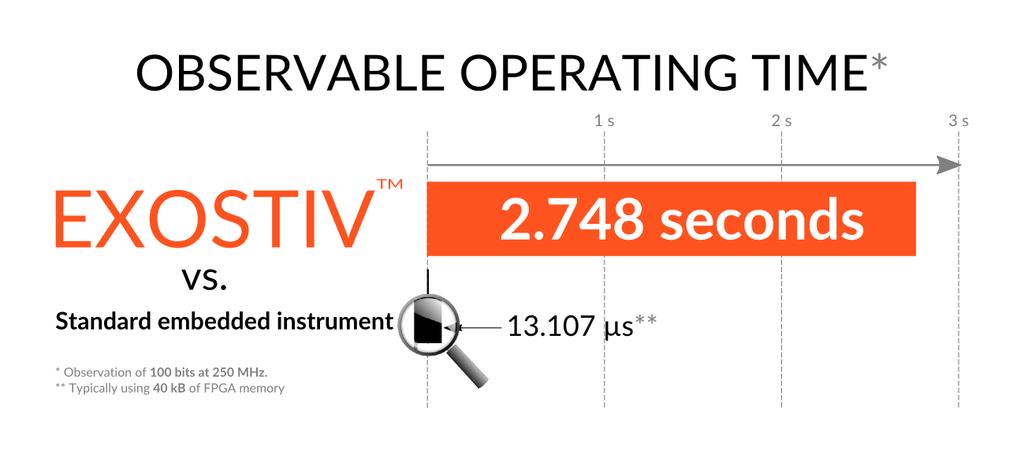
 Reality: 32 kbit RAM is available for debug in the FPGA. = Debug information for 32 frames Equivalent to 1,33 s of a 2 hours movie. Shooting in the dark?")
8 Debugging with an Embedded LA 1) Limit capture to header and controls : bit per frame 2) Worst case : full 2 hours movie at 24 fps: b x 2 h x s x 24 fps = b ~ 22 MB 3) Reality: 32 kbit RAM is available for debug in the FPGA. = Debug information for 32 frames Equivalent to 1,33 s of a 2 hours movie. Shooting in the dark? 4) Solution: we need a more clever triggering approach Question: how do you trigger on something you do not know?
9 What is EXOSTIV TM? EXOSTIV is a new kind of embedded instrument for FPGA debugging EXOSTIV uses a dedicated hardware with high bandwidth and large storage capacity to reach very large observability levels on FPGA during in-lab testing. Debug & Verification Pure Software Emulation & Hardware Acceleration Prototype board & Target board EXOSTIV
10 Problem Today s solutions New solution Due to FPGA complexity, Debugging & Verification times Increase 1. RTL Simulation (SW only) 2. Embedded LA Chipscope / SignalTap (in-lab) 3. Logic Analyzer / Scope (in-lab) Long runtime! Available FPGA memory Available I/Os Limited width Board issues with parallel bus At speed sampling...? EXOSTIV = embedded instrument 1. Transceivers (MGT) JTAG 2. Deep external memory 3. At speed (sampling & execution) 4. Analysis tools for (very) large traces


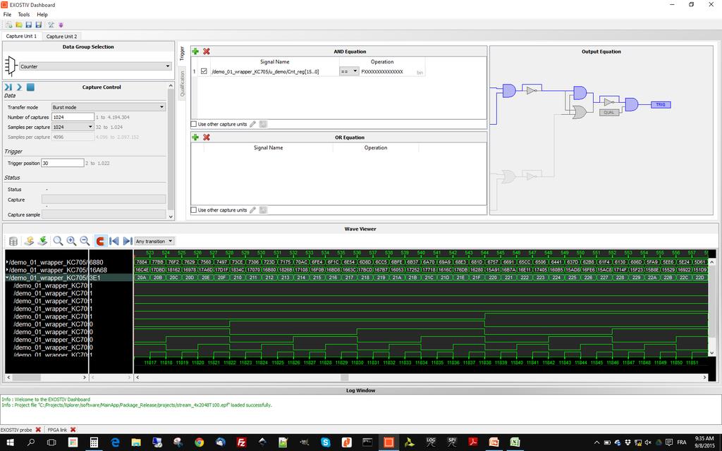
11 EXOSTIV TM - Overview Reach internal nodes Up to 16 capture units Up to 16 data sets per CU 1 trigger + 1 qualification unit per CU Up to nets per data set IP RAM does not grow with capture size system speed Extract trace Up to 8 GB for trace storage Up to 4 x 12.5 Gbps bandwidth Uses Multi Gigabit Transceivers HDMI and SFP+ cage connector Optional connector adapters Downstream channel for IP control USB 3.0 connection with workstation Control & Analyze IP configuration & insertion Trigger and data filter set up IP communication and control Trace reception and encoding Advanced waveform viewer
12

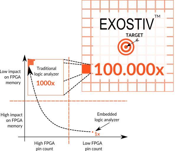
13 Indicative gain


14 EXOSTIV TM - Probe Power button Extra downstream control connector High-speed connector HDMI format up to 4 x 6.6 Gbps Status LED High-speed connector SFP+ format up to 4 x 6.6 Gbps DC power jack USB 3.0

15 EXOSTIV TM in Vivado flow System-level HDL Synthesis Chipscope definition Debug core insertion EXOSTIV definition Implementation Binary load Chipscope debug EXOSTIV debug
16
 Connection")


17 Demo Overview (1) Connection with EXOSTIV Probe FMC connector + Adapter HDMI input Xilinx Kintex-7 evaluation kit Demo design + EXOSTIV IP in Kintex-7
18 Demo Detail of design & IP 200 MHz CNT (16) RAND (16) SINE(16) + Random glitch generator EXOSTIV IP RAM buffer: 1024 x 16 CU 1 Trig only GTX To EXOSTIV Probe RAM buffer: 1024 x 46 1 x Gbps SDI color BAR (46) MHz Noisy sine CU 2 Trig + Qual. 16 bits used for trigger & as data 30 bits used as data only
19 Thank you - Any questions? FPGA Debug Reloaded
Tutorial 11 ChipscopePro, ISE 10.1 and Xilinx Simulator on the Digilent Spartan-3E board
 Tutorial 11 ChipscopePro, ISE 10.1 and Xilinx Simulator on the Digilent Spartan-3E board Introduction This lab will be an introduction on how to use ChipScope for the verification of the designs done on
Using the KC705 Kintex-7 evaluation kit
 EXOSTIV Using the KC705 Kintex-7 evaluation kit Rev. 1.0.3 - April 11, 2018 http://www.exostivlabs.com 1 Table of Contents EXOSTIV using the KC705 kit...3 Introduction...3 Using EXOSTIV with the KC705
Using SignalTap II in the Quartus II Software
 White Paper Using SignalTap II in the Quartus II Software Introduction The SignalTap II embedded logic analyzer, available exclusively in the Altera Quartus II software version 2.1, helps reduce verification
Certus TM Silicon Debug: Don t Prototype Without It by Doug Amos, Mentor Graphics
 Certus TM Silicon Debug: Don t Prototype Without It by Doug Amos, Mentor Graphics FPGA PROTOTYPE RUNNING NOW WHAT? Well done team; we ve managed to get 100 s of millions of gates of FPGA-hostile RTL running
Galore Systems. Profile
 Galore Systems Profile Mission Statement To provide world-class FPGA tools, Electronic Systems and T&M Equipment with timely and effective Technical support Focus Areas Market Segment Focus Defense and
Logic Analysis Basics
 Logic Analysis Basics September 27, 2006 presented by: Alex Dickson Copyright 2003 Agilent Technologies, Inc. Introduction If you have ever asked yourself these questions: What is a logic analyzer? What
Logic Analysis Basics
 Logic Analysis Basics September 27, 2006 presented by: Alex Dickson Copyright 2003 Agilent Technologies, Inc. Introduction If you have ever asked yourself these questions: What is a logic analyzer? What
SignalTap Analysis in the Quartus II Software Version 2.0
 SignalTap Analysis in the Quartus II Software Version 2.0 September 2002, ver. 2.1 Application Note 175 Introduction As design complexity for programmable logic devices (PLDs) increases, traditional methods
Implementing Audio IP in SDI II on Arria V Development Board
 Implementing Audio IP in SDI II on Arria V Development Board AN-697 Subscribe This document describes a reference design that uses the Audio Embed, Audio Extract, Clocked Audio Input and Clocked Audio
SignalTap Plus System Analyzer
 SignalTap Plus System Analyzer June 2000, ver. 1 Data Sheet Features Simultaneous internal programmable logic device (PLD) and external (board-level) logic analysis 32-channel external logic analyzer 166
Using the KCU105 Kintex Ultrascale evaluation kit
 EXOSTIV Using the KCU105 Kintex Ultrascale evaluation kit Rev. 1.0.2 - October 25, 2017 http://www.exostivlabs.com 1 Table of Contents EXOSTIV using the KCU105 kit... 3 Introduction... 3 Using EXOSTIV
Saving time & money with JTAG
 Saving time & money with JTAG AltiumLive 2017: ANNUAL PCB DESIGN SUMMIT Simon Payne CEO, XJTAG Ltd. Saving time and money with JTAG JTAG / IEEE 1149.X Take-away points Get JTAG right from the start Use
LMH0340/LMH0341 SerDes EVK User Guide
 LMH0340/LMH0341 SerDes EVK User Guide July 1, 2008 Version 1.05 1 1... Overview 3 2... Evaluation Kit (SD3GXLEVK) Contents 3 3... Hardware Setup 4 3.1 ALP100 BOARD (MAIN BOARD) DESCRIPTION 5 3.2 SD340EVK
Zebra2 (PandA) Functionality and Development. Isa Uzun and Tom Cobb
 Functionality and Development. Isa Uzun and Tom Cobb") Zebra2 (PandA) Functionality and Development Isa Uzun and Tom Cobb Control Systems Group 27 April 2016 Outline Part - I ZEBRA and Motivation Hardware Architecture Functional Capabilities Part - II Software
Zebra2 (PandA) Functionality and Development Isa Uzun and Tom Cobb Control Systems Group 27 April 2016 Outline Part - I ZEBRA and Motivation Hardware Architecture Functional Capabilities Part - II Software
On-Chip Instrumentation and In-Silicon Debug Tools for SoC Dr. Neal Stollon HDL Dynamics
 On-Chip Instrumentation and In-Silicon Tools for SoC Dr. Neal Stollon HDL Dynamics neals@hdldynamics.com So What do we mean by On-Chip Instrumentation and In-Silicon? What will this talk cover An Overview
Authentic Time Hardware Co-simulation of Edge Discovery for Video Processing System
 Authentic Time Hardware Co-simulation of Edge Discovery for Video Processing System R. NARESH M. Tech Scholar, Dept. of ECE R. SHIVAJI Assistant Professor, Dept. of ECE PRAKASH J. PATIL Head of Dept.ECE,
Sundance Multiprocessor Technology Limited. Capture Demo For Intech Unit / Module Number: C Hong. EVP6472 Intech Demo. Abstract
 Sundance Multiprocessor Technology Limited EVP6472 Intech Demo Unit / Module Description: Capture Demo For Intech Unit / Module Number: EVP6472-SMT949 Document Issue Number 1.1 Issue Data: 27th April 2012
COE758 Xilinx ISE 9.2 Tutorial 2. Integrating ChipScope Pro into a project
 COE758 Xilinx ISE 9.2 Tutorial 2 ChipScope Overview Integrating ChipScope Pro into a project Conventional Signal Sampling Xilinx Spartan 3E FPGA JTAG 2 ChipScope Pro Signal Sampling Xilinx Spartan 3E FPGA
CHAPTER 3 EXPERIMENTAL SETUP
 CHAPTER 3 EXPERIMENTAL SETUP In this project, the experimental setup comprised of both hardware and software. Hardware components comprised of Altera Education Kit, capacitor and speaker. While software
SERDES Eye/Backplane Demo for the LatticeECP3 Serial Protocol Board User s Guide
 for the LatticeECP3 Serial Protocol Board User s Guide March 2011 UG24_01.4 Introduction This document provides technical information and instructions on using the LatticeECP3 SERDES Eye/Backplane Demo
FPGA Development for Radar, Radio-Astronomy and Communications
 John-Philip Taylor Room 7.03, Department of Electrical Engineering, Menzies Building, University of Cape Town Cape Town, South Africa 7701 Tel: +27 82 354 6741 email: tyljoh010@myuct.ac.za Internet: http://www.uct.ac.za
VHDL Design and Implementation of FPGA Based Logic Analyzer: Work in Progress
 VHDL Design and Implementation of FPGA Based Logic Analyzer: Work in Progress Nor Zaidi Haron Ayer Keroh +606-5552086 zaidi@utem.edu.my Masrullizam Mat Ibrahim Ayer Keroh +606-5552081 masrullizam@utem.edu.my
Radar Signal Processing Final Report Spring Semester 2017
 Radar Signal Processing Final Report Spring Semester 2017 Full report report by Brian Larson Other team members, Grad Students: Mohit Kumar, Shashank Joshil Department of Electrical and Computer Engineering
Sundance Multiprocessor Technology Limited. Capture Demo For Intech Unit / Module Number: C Hong. EVP6472 Intech Demo. Abstract
 Sundance Multiprocessor Technology Limited EVP6472 Intech Demo Unit / Module Description: Capture Demo For Intech Unit / Module Number: EVP6472-SMT909 Document Issue Number 1.1 Issue Data: 25th Augest
Prototyping Solutions For New Wireless Standards
 Prototyping Solutions For New Wireless Standards Christoph Juchems IAF Institute For Applied Radio System Technology Berliner Str. 52 J D-38104 Braunschweig Germany www.iaf-bs.de Introduction IAF Institute
Solutions to Embedded System Design Challenges Part II
 Solutions to Embedded System Design Challenges Part II Time-Saving Tips to Improve Productivity In Embedded System Design, Validation and Debug Hi, my name is Mike Juliana. Welcome to today s elearning.
University of Pennsylvania Department of Electrical and Systems Engineering. Digital Design Laboratory. Lab8 Calculator
 University of Pennsylvania Department of Electrical and Systems Engineering Digital Design Laboratory Purpose Lab Calculator The purpose of this lab is: 1. To get familiar with the use of shift registers
Laboratory 4. Figure 1: Serdes Transceiver
 Laboratory 4 The purpose of this laboratory exercise is to design a digital Serdes In the first part of the lab, you will design all the required subblocks for the digital Serdes and simulate them In part
THE DIAGNOSTICS BACK END SYSTEM BASED ON THE IN HOUSE DEVELOPED A DA AND A D O BOARDS
 THE DIAGNOSTICS BACK END SYSTEM BASED ON THE IN HOUSE DEVELOPED A DA AND A D O BOARDS A. O. Borga #, R. De Monte, M. Ferianis, L. Pavlovic, M. Predonzani, ELETTRA, Trieste, Italy Abstract Several diagnostic
SERDES Eye/Backplane Demo for the LatticeECP3 Versa Evaluation Board User s Guide
 SERDES Eye/Backplane Demo for the LatticeECP3 Versa Evaluation Board User s Guide May 2011 UG44_01.1 Introduction This document provides technical information and instructions on using the LatticeECP3
FPGA-BASED EDUCATIONAL LAB PLATFORM
 FPGA-BASED EDUCATIONAL LAB PLATFORM Mircea Alexandru DABÂCAN, Clint COLE Mircea Dabâcan is with Technical University of Cluj-Napoca, Electronics and Telecommunications Faculty, Applied Electronics Department,
Programmable Logic Design Techniques II
 Programmable Logic Design Techniques II. p. 1 Programmable Logic Design Techniques II Almost all digital signal processing requires that information is recorded, possibly manipulated and then stored in
DEDICATED TO EMBEDDED SOLUTIONS
 DEDICATED TO EMBEDDED SOLUTIONS DESIGN SAFE FPGA INTERNAL CLOCK DOMAIN CROSSINGS ESPEN TALLAKSEN DATA RESPONS SCOPE Clock domain crossings (CDC) is probably the worst source for serious FPGA-bugs that
DMC550 Technical Reference
 DMC550 Technical Reference 2002 DSP Development Systems DMC550 Technical Reference 504815-0001 Rev. B September 2002 SPECTRUM DIGITAL, INC. 12502 Exchange Drive, Suite 440 Stafford, TX. 77477 Tel: 281.494.4505
AN 848: Implementing Intel Cyclone 10 GX Triple-Rate SDI II with Nextera FMC Daughter Card Reference Design
 AN 848: Implementing Intel Cyclone 10 GX Triple-Rate SDI II with Nextera FMC Daughter Card Reference Design Updated for Intel Quartus Prime Design Suite: 18.0 Subscribe Send Feedback Latest document on
EEM Digital Systems II
 ANADOLU UNIVERSITY DEPARTMENT OF ELECTRICAL AND ELECTRONICS ENGINEERING EEM 334 - Digital Systems II LAB 3 FPGA HARDWARE IMPLEMENTATION Purpose In the first experiment, four bit adder design was prepared
FPGA Development Techniques. Wednesday November 3, 2004 Polytech Orléans
 FPGA Development Techniques Wednesday November 3, 2004 Polytech Orléans Agenda Static Timing Analysis Constraining an FPGA design and ensuring it meets performance requirements On-Chip Debugging Using
ECE532 Digital System Design Title: Stereoscopic Depth Detection Using Two Cameras. Final Design Report
 ECE532 Digital System Design Title: Stereoscopic Depth Detection Using Two Cameras Group #4 Prof: Chow, Paul Student 1: Robert An Student 2: Kai Chun Chou Student 3: Mark Sikora April 10 th, 2015 Final
LogiCORE IP Spartan-6 FPGA Triple-Rate SDI v1.0
 LogiCORE IP Spartan-6 FPGA Triple-Rate SDI v1.0 DS849 June 22, 2011 Introduction The LogiCORE IP Spartan -6 FPGA Triple-Rate SDI interface solution provides receiver and transmitter interfaces for the
ASTRIX ASIC Microelectronics Presentation Days
 ASTRIX ASIC Microelectronics Presentation Days ESTEC, Noordwijk, 4 th and 5 th February 2004 Matthieu Dollon matthieu.dollon@astrium.eads.net Franck Koebel franck.koebel@astrium.eads.net Page 1 - ESA 4
Nutaq. PicoDigitizer-125. Up to 64 Channels, 125 MSPS ADCs, FPGA-based DAQ Solution With Up to 32 Channels, 1000 MSPS DACs PRODUCT SHEET. nutaq.
 Nutaq Up to 64 Channels, 125 MSPS ADCs, FPGA-based DAQ Solution With Up to 32 Channels, 1000 MSPS DACs PRODUCT SHEET QUEBEC I MONTREAL I N E W YO R K I nutaq.com Nutaq The PicoDigitizer 125-Series is a
2.6 Reset Design Strategy
 2.6 Reset esign Strategy Many design issues must be considered before choosing a reset strategy for an ASIC design, such as whether to use synchronous or asynchronous resets, will every flipflop receive
AN 776: Intel Arria 10 UHD Video Reference Design
 AN 776: Intel Arria 10 UHD Video Reference Design Subscribe Send Feedback Latest document on the web: PDF HTML Contents Contents 1 Intel Arria 10 UHD Video Reference Design... 3 1.1 Intel Arria 10 UHD
Ilmenau, 9 Dec 2016 Testing and programming PCBA s. 1 JTAG Technologies
 Ilmenau, 9 Dec 206 Testing and programming PCBA s JTAG Technologies The importance of Testing Don t ship bad products to your customers, find problems before they do. DOA s (Death On Arrival) lead to huge
Prototyping an ASIC with FPGAs. By Rafey Mahmud, FAE at Synplicity.
 Prototyping an ASIC with FPGAs By Rafey Mahmud, FAE at Synplicity. With increased capacity of FPGAs and readily available off-the-shelf prototyping boards sporting multiple FPGAs, it has become feasible
Altera's 28-nm FPGAs Optimized for Broadcast Video Applications
 Altera's 28-nm FPGAs Optimized for Broadcast Video Applications WP-01163-1.0 White Paper This paper describes how Altera s 40-nm and 28-nm FPGAs are tailored to help deliver highly-integrated, HD studio
JTAG-SMT1 Programming Module for Xilinx FPGAs. Overview. 23 mm. 21.5mm. Revised November 21, 2017 This manual applies to the JTAG-SMT1 rev.
 1300 Henley Court Pullman, WA 99163 509.334.6306 www.digilentinc.com JTAG-SMT1 Programming Module for Xilinx FPGAs Revised November 21, 2017 This manual applies to the JTAG-SMT1 rev. A Overview The JTAG-SMT1
FPGA Laboratory Assignment 4. Due Date: 06/11/2012
 FPGA Laboratory Assignment 4 Due Date: 06/11/2012 Aim The purpose of this lab is to help you understanding the fundamentals of designing and testing memory-based processing systems. In this lab, you will
OF AN ADVANCED LUT METHODOLOGY BASED FIR FILTER DESIGN PROCESS
 IMPLEMENTATION OF AN ADVANCED LUT METHODOLOGY BASED FIR FILTER DESIGN PROCESS 1 G. Sowmya Bala 2 A. Rama Krishna 1 PG student, Dept. of ECM. K.L.University, Vaddeswaram, A.P, India, 2 Assistant Professor,
How to overcome/avoid High Frequency Effects on Debug Interfaces Trace Port Design Guidelines
 How to overcome/avoid High Frequency Effects on Debug Interfaces Trace Port Design Guidelines An On-Chip Debugger/Analyzer (OCD) like isystem s ic5000 (Figure 1) acts as a link to the target hardware by
7 Nov 2017 Testing and programming PCBA s
 7 Nov 207 Testing and programming PCBA s Rob Staals JTAG Technologies Email: robstaals@jtag.com JTAG Technologies The importance of Testing Don t ship bad products to your customers, find problems before
FPGA Prototyping using Behavioral Synthesis for Improving Video Processing Algorithm and FHD TV SoC Design Masaru Takahashi
 FPGA Prototyping using Behavioral Synthesis for Improving Video Processing Algorithm and FHD TV SoC Design Masaru Takahashi SoC Software Platform Division, Renesas Electronics Corporation January 28, 2011
ChipScope Pro Serial I/O Toolkit User Guide
 ChipScope Pro Serial I/O Toolkit User Guide (ChipScope Pro Software 9.2i) R R Xilinx is disclosing this Document and Intellectual Property (hereinafter the Design ) to you for use in the development of
Image generator. Hardware Specification
 Image generator [SVO-03] Rev. NetVision Co., Ltd. Update History Revision Date Note 2018/07/02 New File(Equivalent to Japanese version 1.2) S.Usuba i index 1. Outline... 1 1.1. features and specification
16 Universe LED Matrix Panels Instructions
 Congratulations on buying the high performance LED matrix controller. Eight matrix LED panels 16x32 (8 to 1 scan) Four/Two LED panels 32x32 or 32x64 (16 to 1 scan) Full 24 bit color for 16 million colors,
UNIVERSITY OF TORONTO JOÃO MARCUS RAMOS BACALHAU GUSTAVO MAIA FERREIRA HEYANG WANG ECE532 FINAL DESIGN REPORT HOLE IN THE WALL
 UNIVERSITY OF TORONTO JOÃO MARCUS RAMOS BACALHAU GUSTAVO MAIA FERREIRA HEYANG WANG ECE532 FINAL DESIGN REPORT HOLE IN THE WALL Toronto 2015 Summary 1 Overview... 5 1.1 Motivation... 5 1.2 Goals... 5 1.3
DC Ultra. Concurrent Timing, Area, Power and Test Optimization. Overview
 DATASHEET DC Ultra Concurrent Timing, Area, Power and Test Optimization DC Ultra RTL synthesis solution enables users to meet today s design challenges with concurrent optimization of timing, area, power
University of Victoria. Department of Electrical and Computer Engineering. CENG 290 Digital Design I Lab Manual
 University of Victoria Department of Electrical and Computer Engineering CENG 290 Digital Design I Lab Manual INDEX Introduction to the labs Lab1: Digital Instrumentation Lab2: Basic Digital Components
An FPGA Platform for Demonstrating Embedded Vision Systems. Ariana Eisenstein
 An FPGA Platform for Demonstrating Embedded Vision Systems by Ariana Eisenstein B.S., Massachusetts Institute of Technology (2015) Submitted to the Department of Electrical Engineering and Computer Science
Remote Diagnostics and Upgrades
 Remote Diagnostics and Upgrades Tim Pender -Eastman Kodak Company 10/03/03 About this Presentation Motivation for Remote Diagnostics Reduce Field Maintenance costs Product needed to support 100 JTAG chains
1 Terasic Inc. D8M-GPIO User Manual
 1 Chapter 1 D8M Development Kit... 4 1.1 Package Contents... 4 1.2 D8M System CD... 5 1.3 Assemble the Camera... 5 1.4 Getting Help... 6 Chapter 2 Introduction of the D8M Board... 7 2.1 Features... 7 2.2
Memec Spartan-II LC User s Guide
 Memec LC User s Guide July 21, 2003 Version 1.0 1 Table of Contents Overview... 4 LC Development Board... 4 LC Development Board Block Diagram... 6 Device... 6 Clock Generation... 7 User Interfaces...
Serial Digital Interface II Reference Design for Stratix V Devices
 Serial Digital Interface II Reference Design for Stratix V Devices AN-673 Application Note This document describes the Altera Serial Digital Interface (SDI) II reference design that demonstrates how you
CprE 488 Embedded Systems Design
 CprE 488 Embedded Systems Design MP-2: Digital Camera Design Assigned: Monday of Week 6 Due: Monday of Week 8 Points: 100 + bonus for additional camera features [Note: at this point in the semester you
A Low Power Implementation of H.264 Adaptive Deblocking Filter Algorithm
 A Low Power Implementation of H.264 Adaptive Deblocking Filter Algorithm Mustafa Parlak and Ilker Hamzaoglu Faculty of Engineering and Natural Sciences Sabanci University, Tuzla, 34956, Istanbul, Turkey
Laboratory Exercise 4
 Laboratory Exercise 4 Polling and Interrupts The purpose of this exercise is to learn how to send and receive data to/from I/O devices. There are two methods used to indicate whether or not data can be
16 Dec Testing and Programming PCBA s. 1 JTAG Technologies
 6 Dec 24 Testing and Programming PCBA s JTAG Technologies The importance of Testing Don t ship bad products to your customers, find problems before they do. DOA s (Death On Arrival) lead to huge costs
Teletext Inserter Firmware. User s Manual. Contents
 Teletext Inserter Firmware User s Manual Contents 0 Definition 3 1 Frontpanel 3 1.1 Status Screen.............. 3 1.2 Configuration Menu........... 4 2 Controlling the Teletext Inserter via RS232 4 2.1
Laboratory 1 - Introduction to Digital Electronics and Lab Equipment (Logic Analyzers, Digital Oscilloscope, and FPGA-based Labkit)
") Massachusetts Institute of Technology Department of Electrical Engineering and Computer Science 6. - Introductory Digital Systems Laboratory (Spring 006) Laboratory - Introduction to Digital Electronics
Massachusetts Institute of Technology Department of Electrical Engineering and Computer Science 6. - Introductory Digital Systems Laboratory (Spring 006) Laboratory - Introduction to Digital Electronics
Copyright 2018 Lev S. Kurilenko
 Copyright 2018 Lev S. Kurilenko FPGA Development of an Emulator Framework and a High Speed I/O Core for the ITk Pixel Upgrade Lev S. Kurilenko A thesis submitted in partial fulfillment of the requirements
LogiCORE IP Video Timing Controller v3.0
 LogiCORE IP Video Timing Controller v3.0 Product Guide Table of Contents Chapter 1: Overview Standards Compliance....................................................... 6 Feature Summary............................................................
4-Ch. 250 MHz, 16-bit A/D, 2-Ch. 800 MHz, 16-bit D/A - FMC
 New! Model 3312 Features Four -bit s One digital upconverter Two 800 MHz -bit D/As Sample clock synchronization an external system reference VITA 57 FMC compatible Complete radar or software radio interface
C ch optical MADI & AoIP I/O. MASTER mode: A C8000 frame may be clocked via MADI input or AES67 network. AoIP Dante Brooklin II OEM module
 features Interface for AoIP (AES67 or DANTE) Two AoIP network ports for redundant or switch operation MADI I/O connection Optical SFP module / LC connectors (multi mode or single mode fiber) BNC parallel
Leveraging Reconfigurability to Raise Productivity in FPGA Functional Debug
 Leveraging Reconfigurability to Raise Productivity in FPGA Functional Debug Abstract We propose new hardware and software techniques for FPGA functional debug that leverage the inherent reconfigurability
ASNT_PRBS20B_1 18Gbps PRBS7/15 Generator Featuring Jitter Insertion, Selectable Sync, and Output Amplitude Control
 ASNT_PRBS20B_1 18Gbps PRBS7/15 Generator Featuring Jitter Insertion, Selectable Sync, and Output Amplitude Control Broadband frequency range from 20Mbps 18.0Gbps Minimal insertion jitter Fast rise and
Virtex-II Pro and VxWorks for Embedded Solutions. Systems Engineering Group
 Virtex-II Pro and VxWorks for Embedded Solutions Systems Engineering Group Embedded System Development Embedded Solutions Key components of Embedded systems development Integrated development environment
Digital Blocks Semiconductor IP
 Digital Blocks Semiconductor IP General Description The Digital Blocks IP Core decodes an ITU-R BT.656 digital video uncompressed NTSC 720x486 (525/60 Video System) and PAL 720x576 (625/50 Video System)
C8000. switch over & ducking
 features Automatic or manual Switch Over or Fail Over in case of input level loss. Ducking of a main stereo or surround sound signal by a line level microphone or by a pre recorded announcement / ad input.
Microprocessor Design
 Microprocessor Design Principles and Practices With VHDL Enoch O. Hwang Brooks / Cole 2004 To my wife and children Windy, Jonathan and Michelle Contents 1. Designing a Microprocessor... 2 1.1 Overview
TABLE 3. MIB COUNTER INPUT Register (Write Only) TABLE 4. MIB STATUS Register (Read Only)
 TABLE 4. MIB STATUS Register (Read Only)") TABLE 3. MIB COUNTER INPUT Register (Write Only) at relative address: 1,000,404 (Hex) Bits Name Description 0-15 IRC[15..0] Alternative for MultiKron Resource Counters external input if no actual external
TABLE 3. MIB COUNTER INPUT Register (Write Only) at relative address: 1,000,404 (Hex) Bits Name Description 0-15 IRC[15..0] Alternative for MultiKron Resource Counters external input if no actual external
SingMai Electronics SM06. Advanced Composite Video Interface: HD-SDI to acvi converter module. User Manual. Revision 0.
 SM06 Advanced Composite Video Interface: HD-SDI to acvi converter module User Manual Revision 0.4 1 st May 2017 Page 1 of 26 Revision History Date Revisions Version 17-07-2016 First Draft. 0.1 28-08-2016
Design and Implementation of SOC VGA Controller Using Spartan-3E FPGA
 Design and Implementation of SOC VGA Controller Using Spartan-3E FPGA 1 ARJUNA RAO UDATHA, 2 B.SUDHAKARA RAO, 3 SUDHAKAR.B. 1 Dept of ECE, PG Scholar, 2 Dept of ECE, Associate Professor, 3 Electronics,
Xilinx Answer Eye Qualification
 Xilinx Answer 70915 Eye Qualification Important Note: This downloadable PDF of an Answer Record is provided to enhance its usability and readability. It is important to note that Answer Records are Web-based
Lab #10 Hexadecimal-to-Seven-Segment Decoder, 4-bit Adder-Subtractor and Shift Register. Fall 2017
 University of Texas at El Paso Electrical and Computer Engineering Department EE 2169 Laboratory for Digital Systems Design I Lab #10 Hexadecimal-to-Seven-Segment Decoder, 4-bit Adder-Subtractor and Shift
Polar Decoder PD-MS 1.1
 Product Brief Polar Decoder PD-MS 1.1 Main Features Implements multi-stage polar successive cancellation decoder Supports multi-stage successive cancellation decoding for 16, 64, 256, 1024, 4096 and 16384
A Briefing on IEEE Standard Test Access Port And Boundary-Scan Architecture ( AKA JTAG )
") A Briefing on IEEE 1149.1 1990 Standard Test Access Port And Boundary-Scan Architecture ( AKA JTAG ) Summary With the advent of large Ball Grid Array (BGA) and fine pitch SMD semiconductor devices the
A Briefing on IEEE 1149.1 1990 Standard Test Access Port And Boundary-Scan Architecture ( AKA JTAG ) Summary With the advent of large Ball Grid Array (BGA) and fine pitch SMD semiconductor devices the
Keysight Technologies CAN/LIN Measurements (Option AMS) for InfiniiVision Series Oscilloscopes
 for InfiniiVision Series Oscilloscopes") Ihr Spezialist für Mess- und Prüfgeräte Keysight Technologies CAN/LIN Measurements (Option AMS) for InfiniiVision Series Oscilloscopes Data Sheet Introduction Debug the signal integrity of your CAN and
Ihr Spezialist für Mess- und Prüfgeräte Keysight Technologies CAN/LIN Measurements (Option AMS) for InfiniiVision Series Oscilloscopes Data Sheet Introduction Debug the signal integrity of your CAN and
Modeling and Implementing Software-Defined Radio Communication Systems on FPGAs Puneet Kumar Senior Team Lead - SPC
 Modeling and Implementing Software-Defined Radio Communication Systems on FPGAs Puneet Kumar Senior Team Lead - SPC 2012 The MathWorks, Inc. 1 Agenda Integrated Model-Based Design to Implement SDR on FPGA
SingMai Electronics SM06. Advanced Composite Video Interface: DVI/HD-SDI to acvi converter module. User Manual. Revision th December 2016
 SM06 Advanced Composite Video Interface: DVI/HD-SDI to acvi converter module User Manual Revision 0.3 30 th December 2016 Page 1 of 23 Revision History Date Revisions Version 17-07-2016 First Draft. 0.1
Display Interfaces. Display solutions from Inforce. MIPI-DSI to Parallel RGB format
 Display Interfaces Snapdragon processors natively support a few popular graphical displays like MIPI-DSI/LVDS and HDMI or a combination of these. HDMI displays that output any of the standard resolutions
Scalable, intelligent image processing board for highest requirements on image acquisition and processing over long distances by optical connection
 i Product Profile of Scalable, intelligent image processing board for highest requirements on image acquisition and processing over long distances by optical connection First Camera Link HS F2 Frame grabber
18 Nov 2015 Testing and Programming PCBA s. 1 JTAG Technologies
 8 Nov 25 Testing and Programming PCBA s JTAG Technologies The importance of Testing Don t ship bad products to your customers, find problems before they do. DOA s (Death On Arrival) lead to huge costs
FPGA Design with VHDL
 FPGA Design with VHDL Justus-Liebig-Universität Gießen, II. Physikalisches Institut Ming Liu Dr. Sören Lange Prof. Dr. Wolfgang Kühn ming.liu@physik.uni-giessen.de Lecture Digital design basics Basic logic
CSCB58 - Lab 4. Prelab /3 Part I (in-lab) /1 Part II (in-lab) /1 Part III (in-lab) /2 TOTAL /8
 /1 Part II (in-lab) /1 Part III (in-lab) /2 TOTAL /8") CSCB58 - Lab 4 Clocks and Counters Learning Objectives The purpose of this lab is to learn how to create counters and to be able to control when operations occur when the actual clock rate is much faster.
CSCB58 - Lab 4 Clocks and Counters Learning Objectives The purpose of this lab is to learn how to create counters and to be able to control when operations occur when the actual clock rate is much faster.
EE178 Lecture Module 4. Eric Crabill SJSU / Xilinx Fall 2005
 EE178 Lecture Module 4 Eric Crabill SJSU / Xilinx Fall 2005 Lecture #9 Agenda Considerations for synchronizing signals. Clocks. Resets. Considerations for asynchronous inputs. Methods for crossing clock
LAX_x Logic Analyzer
 Legacy documentation LAX_x Logic Analyzer Summary This core reference describes how to place and use a Logic Analyzer instrument in an FPGA design. Core Reference CR0103 (v2.0) March 17, 2008 The LAX_x
MODULAR DIGITAL ELECTRONICS TRAINING SYSTEM
 MODULAR DIGITAL ELECTRONICS TRAINING SYSTEM MDETS UCTECH's Modular Digital Electronics Training System is a modular course covering the fundamentals, concepts, theory and applications of digital electronics.
DE2-115/FGPA README. 1. Running the DE2-115 for basic operation. 2. The code/project files. Project Files
 DE2-115/FGPA README For questions email: jeff.nicholls.63@gmail.com (do not hesitate!) This document serves the purpose of providing additional information to anyone interested in operating the DE2-115
APPLICATION NOTE 4312 Getting Started with DeepCover Secure Microcontroller (MAXQ1850) EV KIT and the CrossWorks Compiler for the MAXQ30
 EV KIT and the CrossWorks Compiler for the MAXQ30") Maxim > Design Support > Technical Documents > Application Notes > Microcontrollers > APP 4312 Keywords: MAXQ1850, MAXQ1103, DS5250, DS5002, microcontroller, secure microcontroller, uc, DES, 3DES, RSA,
Maxim > Design Support > Technical Documents > Application Notes > Microcontrollers > APP 4312 Keywords: MAXQ1850, MAXQ1103, DS5250, DS5002, microcontroller, secure microcontroller, uc, DES, 3DES, RSA,
MSO-28 Oscilloscope, Logic Analyzer, Spectrum Analyzer
 Link Instruments Innovative Test & Measurement solutions since 1986 Store Support Oscilloscopes Logic Analyzers Pattern Generators Accessories MSO-28 Oscilloscope, Logic Analyzer, Spectrum Analyzer $ The