SV1C Personalized SerDes Tester. Data Sheet
|
|
|
- Elijah Welch
- 5 years ago
- Views:
Transcription

1 SV1C Personalized SerDes Tester Data Sheet
2 Table of Contents 1
3 Table of Contents Table of Contents Table of Contents... 2 List of Figures... 3 List of Tables... 3 Introduction... 4 Overview... 4 Key Benefits... 4 Applications... 5 Physical Connectors... 5 Features... 6 Multi-Lane Loopback... 6 Multiple-Source Jitter Injection... 6 Pre-Emphasis Generation... 8 Programmable SSC Generation and Frequency Synthesis... 9 Per-Lane Clock Recovery and Unique Dual-Path Architecture... 9 Auxiliary Control Port Analysis Automation Specifications
4 Table of Contents List of Figures Figure 1 SV1C connectors... 5 Figure 2 Illustration of loopback applications Figure 3 Illustration of calibrated jitter waveform Figure 4 Illustration of jitter tolerance curve Figure 5 Illustration of pre-emphasis design Figure 6 Illustration of multiple waveform shapes that can be synthesized using the pre-emphasis function of the SV1C Figure 7 Programmable SSC generation... 9 Figure 8 Per-lane clock recovery and dual-path architecture Figure 9 Photograph of the auxiliary control port on the SV1C Figure 10 Sampling of analysis and report windows Figure 11 Screen capture of IntrospectESP user environment List of Tables Table 1 General Specifications Table 2 Transmitter Characteristics Table 3 Receiver Characteristics Table 4 Clocking Characteristics Table 5 Pattern Handling Characteristics Table 6 Measurement and Throughput Characteristics Table 7 Instruction Sequence Cache Table 8 DUT Control Capabilities
5 Introduction and Features Introduction Overview The SV1C Personalized SerDes Tester is an ultra-portable, high-performance instrument that creates a new category of tool for high-speed digital product engineering teams. It integrates multiple technologies in order to enable the self-contained test and measurement of complex SerDes interfaces such as PCI Express Gen 3, MIPI M-PHY, Thunderbolt, or USB3. Coupled with a seamless, easy-to-use development environment, this tool enables product engineers with widely varying skills to efficiently work with and develop SerDes verification algorithms. The SV1C fits in one hand and contains 8 independent stimulus generation ports, 8 independent capture and measurement ports and various clocking, synchronization and lane-expansion capabilities. It has been designed specifically to address the growing need of a parallel, system-oriented test methodology while offering world-class signal-integrity features such as jitter injection and jitter measurement. With a small form factor, an extensive signal-integrity feature set, and an exceptionally powerful software development environment, the SV1C is not only suitable for signal-integrity verification engineers that perform traditional characterization tasks, but it is also ideal for FPGA developers and software developers who need rapid turnaround signal verification tools or hardwaresoftware interoperability confirmation tools. The SV1C integrates state of the art functions such as digital data capture, bit error rate measurement, clock recovery, jitter decomposition and jitter generation. Key Benefits True parallel bit-error-rate measurement across 8 lanes Fully-synthesized integrated jitter injection on all lanes Fully-automated integrated jitter testing on all lanes Optimized pattern generator rise-time for receiver stress test applications Flexible pre-emphasis and equalization Flexible loopback support per lane Hardware clock recovery per lane State of the art programming environment based on the highly intuitive Python language Integrated device control through SPI, I2C, or JTAG Reconfigurable, protocol customization (on request) 4

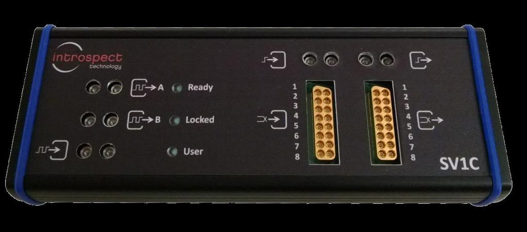
6 Applications Introduction and Features Physical Connectors Parallel PHY validation of serial bus standards such as: PCI Express (PCIe) HDMI UHS-2 Thunderbolt MIPI M-PHY XAUI CPRI JESD204B USB SATA Interface test of electrical/optical media such as: Backplane Cable CFP MSA, SFP MSA, SFP+ MSA Plug-and-play system-level validation such as: PCI Express DisplayPort sink/source MIPI M-PHY Timing verification: PLL transfer function measurement Clock recovery bandwidth verification Frequency ppm offset characterization Mixed-technology applications: High-speed ADC and DAC (JESD204) data capture and/or synthesis FPGA-based system development Channel and device emulation Clock-recovery triggering for external oscilloscope or BERT equipment Figure 1 shows the high-speed differential transmit and receive data pins, reference clock connectors, power and USB ports on the SV1C chassis. The auxiliary triggers and programmable SCSI ports are optional features. Figure 1 SV1C connectors 5


 to the DUT while stressing the DUT receiver with jitter, skew, or voltage swing.")
7 Introduction and Features Features Multi-Lane Loopback The SV1C is the only bench-top tool that offers instrument-grade loopback capability on all differential lanes. The loopback capability of the SV1C includes: Retiming of data for the purpose of decoupling DUT receiver performance from DUT transmitter performance Arbitrary jitter or voltage swing control on loopback data Figure 2 shows two common loopback configurations that can be used with the SV1C. In the first configuration, a single DUT s transmitter and receiver channels are connected together through the SV1C. In the second configuration, arbitrary pattern testing can be performed on an end-to-end communications link. The SV1C is used to pass data through from a traffic generator (such as an endpoint on a real system board) to the DUT while stressing the DUT receiver with jitter, skew, or voltage swing. (a) (b) Figure 2 Illustration of loopback applications. Multiple-Source Jitter Injection The SV1C is capable of generating calibrated jitter stress on any data pattern and any output lane configuration. Sinusoidal jitter injection is calibrated in the time and frequency domain in order to generate high-purity stimulus signals as shown in Figure 3. 6


8 Introduction and Features Figure 3 Illustration of calibrated jitter waveform. The jitter injection feature is typically exploited in order to perform automated jitter tolerance testing as shown in the example in Figure 4. As is the case for other features in the SV1C Personalized SerDes Tester, jitter tolerance testing happens in parallel across all lanes. For advanced applications, the SV1C also includes RJ injection and a third-source arbitrary waveform jitter synthesizer. Figure 4 Illustration of jitter tolerance curve. 7
9 Introduction and Features Pre-Emphasis Generation Conventionally offered as a separate instrument, per-lane pre-emphasis control is integrated on the 8-lane SV1C tester. The user can individually set the transmitter pre-emphasis using a built-in Tap structure. Pre-emphasis allows the user to optimize signal characteristics at the DUT input pins. Each transmitter in the SV1C implements a discrete-time linear equalizer as part of the driver circuit. An illustration of such equalizer is shown in Figure 5, and sample synthesized waveform shapes are shown in Figure 6. Figure 5 Illustration of pre-emphasis design. Figure 6 Illustration of multiple waveform shapes that can be synthesized using the pre-emphasis function of the SV1C. 8

10 Introduction and Features Programmable SSC Generation and Frequency Synthesis The SV1C incorporates precision frequency synthesis technology that allows for the generation of programmable SSC waveforms at any data rate. The SSC waveforms are superimposed on the pattern generator outputs, and they coexist with other jitter injection sources of the SV1C. Thus, a truly complete jitter cocktail can be produced for the most thorough receiver validation. Figure 7 illustrates the SSC capability of the SV1C. In the figure, the SV1C is programmed to synthesize four slightly different modulation frequencies showcasing the precision programmability of the tool. Figure 7 Programmable SSC generation. Per-Lane Clock Recovery and Unique Dual-Path Architecture Like pre-emphasis, conventional tools often require separate clock recovery instrumentation. In the SV1C, each receiver has its own embedded analog clock recovery circuit. Additionally, the clock recovery is monolithically integrated directly inside the receiver s high-speed sampler, thus offering the lowest possible sampling latency in a test and measurement instrument. The user does not have to make special connections or carefully match cable lengths. The monolithic nature of the SV1C clock recovery helps achieve wide tracking bandwidth for measuring signals that possess spread-spectrum clocking or very high amplitude wander. Figure 8 shows a block diagram of the clock recovery capability inside the SV1C Personalized SerDes Tester. 9


11 Introduction and Features Also shown in Figure 8 is the dual-path receiver architecture of the SV1C. This unique architecture allows the SV1C to operate as both a digital capture/analysis instrument and an analog measurement instrument. A feature rich clock management system allows for customization of the SV1C to specific customer requirements. Figure 8 Per-lane clock recovery and dual-path architecture. Auxiliary Control Port The SV1C includes a low-speed auxiliary control port that is based on a standard SCSI connector (Figure 9). This port enables controlling DUT registers through JTAG, I2C, or SPI. Additionally, the port includes reconfigurable trigger and flag capability for synchronizing the SV1C with external tools or events. Figure 9 Photograph of the auxiliary control port on the SV1C. 10
 data from a single input channel against a specified data pattern and reports the bit error count.")
12 Introduction and Features Analysis The SV1C instrument has an independent Bit Error Rate Tester (BERT) for each of its input channels. Each BERT compares recovered (retimed) data from a single input channel against a specified data pattern and reports the bit error count. Apart from error counting, the instrument offers a wide range of measurement and analysis features including: Jitter separation Eye mask testing Voltage level, pre-emphasis level, and signal parameter measurement Frequency measurement and SSC profile extraction Figure 10 illustrates a few of the analysis and reporting features of the SV1C. Starting from the top left and moving in a clock-wise manner, the figure illustrates bathtub acquisition and analysis, waveform capture, raw data viewing, and eye diagram plotting. As always, these analysis options are executed in parallel on all activated lanes. Figure 10 Sampling of analysis and report windows. 11
.")
13 Introduction and Features Automation The SV1C is operated using the award winning IntrospectESP Software. It features a comprehensive scripting language with an intuitive component-based design as shown in the screen shot in Figure 11(a). Component-based design is IntrospectESP s way of organizing the flexibility of the instrument in a manner that allows for easy program development. It highlights to the user only the parameters that are needed for any given task, thus allowing program execution in a matter of minutes. For further help, the SV1C features automatic code generation for common tasks such as Eye Diagram or Bathtub Curve generation as shown in Figure 11(b). (a) (b) Figure 11 Screen capture of IntrospectESP user environment. 12
14 Specifications Specifications Table 1 Ports General Specifications Parameter Value Units Description and Conditions Number of Differential Transmitters 8 Number of Differential Receivers 8 Number of Dedicated Clock Outputs 2 Individually synthesized frequency and output format. Number of Dedicated Clock Inputs 1 Used as external Reference Clock input. Number of Trigger Input Pins Multiple Consult user manual for included capability. Contact factory for customization. Number of Flag Output Pins Multiple Consult user manual for included capability. Contact factory for customization. Data Rates and Frequencies Minimum Programmable Data Rate 1 Mbps Maximum Programmable Data Rate 14 Gbps Maximum Data Rate Purchase Options 4 Gbps 8.5 Gbps 12.5 Gbps 14 Gbps Data Rate Field Upgrade Gbps Contact factory for details. Frequency Resolution of Programmed Data Rate 1 khz Finer resolution is possible. Contact factory for customization. Clock Input Frequency Range Single-ended Input Impedance Common mode/threshold voltage Minimum Differential Voltage Swing Clock Outputs Frequency Range Common mode/threshold voltage Differential Voltage Swing /40/60 1.8V 2.5V 1.95V 200 / /1.2/0.875/0.375/- 0.8/0.35/0.35/0.725/0.86 MHz k V V V mvpp MHz V Vpp Support for LVDS, LVPECL, CML, HCSL, and CMOS. min / typ / max min / typ / max min / typ / max min / typ / max fin < 212.5MHz / fin > 212.5MHz in steps of 1kHz typical LVPECL/LVDS V/LVDS1.8V/HCSL/CML typical LVPECL/LVDS V/LVDS1.8V/HCSL/CML also supports single-ended CMOS format Table 2 Transmitter Characteristics Parameter Value Units Description and Conditions Output Coupling DC common mode voltage 750 mv typical (different offsets are firmware programmable) AC Output Differential Impedance 100 Ohm typical Voltage Performance Minimum Differential Voltage Swing 20 mv Maximum Differential Voltage Swing mvpp mvpp Differential Voltage Swing Resolution 20 mv Mbps to 5 Gbps, 50 ohm AC coupled termination. 5 Gbps to 12.5 Gbps, 50 ohm AC coupled termination. 13
15 Specifications Accuracy of Differential Voltage Swing larger of: +/-10% %, mv of programmed value, and +/- 10mV Rise and Fall Time 50 ps Typical, 500 mvpp signal, 20-80%, 50 ohm AC coupled termination. 75 ps Typical, 500 mvpp signal, 10%-90%, 50 ohm AC coupled termination. Pre-emphasis Performance Pre-Emphasis Pre-Tap Range -4 to +4 db Both high-pass and low-pass functions are available. This is the smallest achievable range based on worstcase conditions. Typical operating conditions result in wider pre-emphasis range. Pre-Emphasis Pre-Tap Resolution Range / 32 db Pre-Emphasis Post1-Tap Range 0 to 6 db Only high-pass function is available. This is the smallest achievable range based on worst-case conditions. Typical operating conditions result in wider preemphasis range. Pre-Emphasis Post1-Tap Resolution Range / 32 db Pre-Emphasis Post2-Tap Range -4 to +4 db Both high-pass and low-pass functions are available. This is the smallest achievable range based on worstcase conditions. Typical operating conditions result in wider pre-emphasis range. Pre-Emphasis Post2-Tap Resolution Range / 32 db Jitter Performance Random Jitter Noise Floor 1000 fs Based on measurement with high-bandwidth scope and with first-order clock recovery. Minimum Frequency of Injected Deterministic Jitter Maximum Frequency of Injected Deterministic Jitter Frequency Resolution of Injected Deterministic Jitter Maximum Peak-to-Peak Injected Deterministic Jitter Magnitude Resolution of Injected Deterministic Jitter 0.1 khz Contact factory for further customization. 80 MHz 0.1 khz Contact factory for further customization ps This specification is separate from low-frequency wander generator and SSC generator. 500 fs Jitter injection is based on multi-resolution synthesizer, so this number is an effective resolution. Internal synthesizer resolution is defined in equivalent number of bits. Injected Deterministic Jitter Setting Per-bank Common across all channels within a bank. Maximum RMS Random Jitter Injection 0.1 UI Magnitude Resolution of Injected Jitter 0.1 ps Accuracy of Injected Jitter Magnitude larger of: +/-10% of programmed value, and +/-10 ps %, ps Injected Random Jitter Setting Common Common across all channels within a bank. Transmitter-to-Transmitter Skew Performance Lane to Lane Integer-UI Minimum Skew -20 UI Lane to Lane Integer-UI Maximum Skew 20 UI Effect of Skew Adjustment on Jitter Injection None Lane to Lane Skew +/- 30 ps 14
16 Table 3 Receiver Characteristics Specifications Input Coupling AC Performance Parameter Value Units Description and Conditions AC Input Differential Impedance 100 Ohm Minimum Detectable Differential Voltage Maximum Allowable Differential Voltage Minimum Programmable Comparator Threshold Voltage Maximum Programmable Comparator Threshold Voltage Differential Comparator Threshold Voltage Resolution Differential Comparator Threshold Voltage Accuracy 25 mv 2000 mv -550 mv +550 mv 10 mv larger of: +/-10% of programmed value, and +/- 10mV %, mv Measured Eye Width Accuracy 10% 15% 25% Maximum error, Mbps 2.0 Gbps, 200 mvpp minimum input amplitude Maximum error, 2.0 Mbps - 5 Gbps, 200 mvpp minimum input amplitude Maximum error, 5 Gbps 12.5 Gbps, 200 mvpp minimum input amplitude Resolution Enhancement & Equalization Jitter Performance DC Gain 0 db 2 db 4 db 6 db 8 db CTLE Maximum Gain 16 db CTLE Resolution 1 db DC Gain Control Equalization Control Input Jitter Noise Floor in System Reference Mode Input Jitter Noise Floor in Extracted Clock Mode Timing Generator Performance Skew Per-receiver Per-receiver 25 ps 10 ps Resolution at Maximum Data Rate mui Resolution (as a percentage of UI) improves for lower data rate. Contact factory for details. Differential Non-Linearity Error +/- 0.5 LSB Integral Non-Linearity Error +/- 5 ps Range Lane to Lane Skew Measurement Accuracy Unlimited +/- 10 ps 15
17 Table 4 Clocking Characteristics Parameter Value Units Description and Conditions Internal Time Base Number of Internal Frequency References 2 Relevant for future customization. Embedded Clock Applications Specifications Transmit Timing Modes System Clock can be extracted from one data receiver channels Extracted to drive all transmitter channels. Receive Timing Modes System All channels have clock recovery for extracted mode Extracted operation. Lane to Lane Tracking Bandwidth 4 MHz Single-Lane CDR Tracking Bandwidth 3-12 MHz Forwarded Clock Applications Transmit Timing Modes System Forwarded Channel 1 acts as forwarded clock for samplers. Receive Timing Modes System Forwarded Channel 1 acts as forwarded clock for samplers. Clock Tracking Bandwidth 4 MHz Second order critically damped response. Spread Spectrum Support Receive Lanes Track SSC Data Yes Requires operation in extracted clock mode. Transmit Lanes Generate SSC Data Yes Consult factory for availability. Minimum Spread 0.1 % Maximum Spread 2 % Spread Programming Resolution 0.01 % Minimum Spreading Frequency 31.5 khz Maximum Spreading Frequency 63 khz 16
18 Table 5 Pattern Handling Characteristics Parameter Value Units Description and Conditions Loopback Rx to Tx Loopback Capability Per channel Lane to Lane Latency Mismatch 0 UI Preset Patterns Standard Built-In Patterns Pattern Choice per Transmit Channel Pattern Choice per Receive Channel All Zeros D21.5 K28.5 K28.7 DIV.16 DIV.20 DIV.40 DIV.50 PRBS.5 PRBS.7 PRBS.9 PRBS.11 PRBS.13 PRBS.15 PRBS.21 PRBS.23 PRBS.31 Per-transmitter Per-receiver Specifications BERT Comparison Mode User Programmable Pattern Memory Automatic seed generation for PRBS Automatically aligns to PRBS data patterns. Total Available Memory 2 GByte Memory allocation is customizable. Contact factory. Individual Force Pattern Individual Expected Pattern Per-transmitter Per-receiver Minimum Pattern Segment Size 512 bits Total Memory Space for Transmitters 1 Mbits Memory allocation is customizable. Contact factory. Total Expected Memory Space for Receivers Pattern Sequencing Sequence Control Number of Sequencer Slots per Pattern Generator Maximum Loop Count per Sequencer Slot Additional Pattern Characteristics Pattern Switching 1 Mbits Memory allocation is customizable. Contact factory. Loop infinite Loop on count Play to end 4 This refers to the number of sequencer slots that can operate at any given time. The instrument has storage space for 16 different sequencer programs Wait to end of segment Immediate Raw Data Capture Length 8192 bits When sourcing PRBS patterns, this option does not exist. 17
19 Table 6 BERT Sync BERT Alignment Measurement and Throughput Characteristics Parameter Value Units Description and Conditions Specifications Alignment Modes Pattern Module can align to any user pattern or preset pattern. PRBS Minimum SYNC Error Threshold 3 bits Maximum SYNC Error Threshold bits Minimum SYNC Sample Count 1024 bits Maximum SYNC Sample Count 2 32 bits SYNC Time 20 ms Assumes a PRBS7 pattern that is stored in a user pattern segment and worst case misalignment between DUT pattern and expected pattern; data rate is 3.25 Gbps. Error Counter Size 32 bits Sample counts in the BERT are programmed in increments of 32 bits. Maximum Single-Shot Duration bits Repeat mode is available to continuously count over longer durations. Continuous Duration Indefinite CDR Lock Time 5 us Self-Alignment Time 50 ms Table 7 Instruction Sequence Cache Parameter Value Units Description and Conditions Simple Instruction Cache Instruction Learn mode Instruction Advanced Instruction Cache Local Instruction Storage Start Stop Replay 1M Instructions Instruction Sequence Segments 1000 Table 8 DUT Control Capabilities Parameter Value Units Description and Conditions DUT IEEE (JTAG) Port (Option) JTAG-Port Transmit Signals JTAG-Port Receive Signals TCK TRST TDI TDO JTAG-Port Transmit Voltage Swing 0 to 2.5 V (Fixed) JTAG-Port Receive Max Voltage Swing 0 to 2.5 V TDI Bit Memory TDO Bit Memory 4k 4k DUT SPI Port (Option) SPI Signals SCLK SSN MISO MOSI Voltage Swing (Fixed) 0 to 2.5 V 18

20 Introspect Technology Revision Number History Date 1.0 Document release Feb 27, Updated jitter injection specs, Oct 07, 2013 SSC specs, clock recovery specs; added block diagram descriptions 1.2 Minor edits Oct 07, Update to specifications Nov 12, Update to specifications Apr 15, Update to specifications; Aug 1, 2014 removed test sequences 1.6 Updated document template Jun 11, Added physical connectors info Mar 11, Update to specifications Nov 30, Update to specifications Apr 07, 2017 The information in this document is subject to change without notice and should not be construed as a commitment by Introspect Technology. While reasonable precautions have been taken, Introspect Technology assumes no responsibility for any errors that may appear in this document. Introspect Technology, 2017 Published on April 07, 2017 EN-D006E-E-17097
SV1C Personalized SerDes Tester
 SV1C Personalized SerDes Tester Data Sheet SV1C Personalized SerDes Tester Data Sheet Revision: 1.0 2013-02-27 Revision Revision History Date 1.0 Document release Feb 27, 2013 The information in this
Combating Closed Eyes Design & Measurement of Pre-Emphasis and Equalization for Lossy Channels
 Combating Closed Eyes Design & Measurement of Pre-Emphasis and Equalization for Lossy Channels Why Test the Receiver? Serial Data communications standards have always specified both the transmitter and
Combating Closed Eyes Design & Measurement of Pre-Emphasis and Equalization for Lossy Channels
 Combating Closed Eyes Design & Measurement of Pre-Emphasis and Equalization for Lossy Channels Why Test the Receiver? Serial Data communications standards have always specified both the transmitter and
32 G/64 Gbaud Multi Channel PAM4 BERT
 Product Introduction 32 G/64 Gbaud Multi Channel PAM4 BERT PAM4 PPG MU196020A PAM4 ED MU196040A Signal Quality Analyzer-R MP1900A Series Outline of MP1900A series PAM4 BERT Supports bit error rate measurements
Datasheet SHF A
 SHF Communication Technologies AG Wilhelm-von-Siemens-Str. 23D 12277 Berlin Germany Phone +49 30 772051-0 Fax ++49 30 7531078 E-Mail: sales@shf.de Web: http://www.shf.de Datasheet SHF 19120 A 2.85 GSa/s
Switching Solutions for Multi-Channel High Speed Serial Port Testing
 Switching Solutions for Multi-Channel High Speed Serial Port Testing Application Note by Robert Waldeck VP Business Development, ASCOR Switching The instruments used in High Speed Serial Port testing are
ASNT_PRBS20B_1 18Gbps PRBS7/15 Generator Featuring Jitter Insertion, Selectable Sync, and Output Amplitude Control
 ASNT_PRBS20B_1 18Gbps PRBS7/15 Generator Featuring Jitter Insertion, Selectable Sync, and Output Amplitude Control Broadband frequency range from 20Mbps 18.0Gbps Minimal insertion jitter Fast rise and
C65SPACE-HSSL Gbps multi-rate, multi-lane, SerDes macro IP. Description. Features
 6.25 Gbps multi-rate, multi-lane, SerDes macro IP Data brief Txdata1_in Tx1_clk Bist1 Rxdata1_out Rx1_clk Txdata2_in Tx2_clk Bist2 Rxdata2_out Rx2_clk Txdata3_in Tx3_clk Bist3 Rxdata3_out Rx3_clk Txdata4_in
Draft Baseline Proposal for CDAUI-8 Chipto-Module (C2M) Electrical Interface (NRZ)
 Electrical Interface (NRZ)") Draft Baseline Proposal for CDAUI-8 Chipto-Module (C2M) Electrical Interface (NRZ) Authors: Tom Palkert: MoSys Jeff Trombley, Haoli Qian: Credo Date: Dec. 4 2014 Presented: IEEE 802.3bs electrical interface
Draft Baseline Proposal for CDAUI-8 Chipto-Module (C2M) Electrical Interface (NRZ) Authors: Tom Palkert: MoSys Jeff Trombley, Haoli Qian: Credo Date: Dec. 4 2014 Presented: IEEE 802.3bs electrical interface
Synthesized Clock Generator
 Synthesized Clock Generator CG635 DC to 2.05 GHz low-jitter clock generator Clocks from DC to 2.05 GHz Random jitter
2016 PDV Conference. Time Alignment of Multiple Real-Time High Bandwidth Scope. Channels
 Time Alignment of Multiple Real-Time High Bandwidth Scope Channels 1 Time Synchronization Between Scope Channels for Data Acquisition Large Acquisition Systems Often Require Synchronization of Multiple
Technical Article MS-2714
 . MS-2714 Understanding s in the JESD204B Specification A High Speed ADC Perspective by Jonathan Harris, applications engineer, Analog Devices, Inc. INTRODUCTION As high speed ADCs move into the GSPS range,
PBR-310C E-BERT. 10Gb/s BERT System with Eye Diagram Tracer
 PBR-310C E-BERT 10Gb/s BERT System with Eye Diagram Tracer rate from 8.5~11.1Gb/s and extend data rate down to 125M~5Gb/s Support up to four channels Eye Diagram and Mask Test* Eye Contour and Histogram*
GALILEO Timing Receiver
 GALILEO Timing Receiver The Space Technology GALILEO Timing Receiver is a triple carrier single channel high tracking performances Navigation receiver, specialized for Time and Frequency transfer application.
Agilent Technologies Pulse Pattern and Data Generators Digital Stimulus Solutions
 Agilent Technologies Pattern and Data Generators Digital Stimulus Solutions Leading pulse, pattern, data and clock generation for all test needs in digital design and manufacturing Pattern Generators Agilent
Keysight Technologies M8048A ISI Channels
 Keysight Technologies M8048A ISI Channels Master Your Next Designs Data Sheet Key features Emulate a wide range of channel loss with cascadable ISI traces with fine resolution 4 short (7.7 to 12.8 ) and
PicoScope 6407 Digitizer
 YE AR PicoScope 6407 Digitizer HIGH PERFORMANCE USB DIGITIZER Programmable and Powerful 1 GHz bandwidth 1 GS buffer size 5 GS/s real-time sampling Advanced digital triggers Built-in function generator
SignalTap Plus System Analyzer
 SignalTap Plus System Analyzer June 2000, ver. 1 Data Sheet Features Simultaneous internal programmable logic device (PLD) and external (board-level) logic analysis 32-channel external logic analyzer 166
MSO-28 Oscilloscope, Logic Analyzer, Spectrum Analyzer
 Link Instruments Innovative Test & Measurement solutions since 1986 Store Support Oscilloscopes Logic Analyzers Pattern Generators Accessories MSO-28 Oscilloscope, Logic Analyzer, Spectrum Analyzer $ The
Receiver Testing to Third Generation Standards. Jim Dunford, October 2011
 Receiver Testing to Third Generation Standards Jim Dunford, October 2011 Agenda 1.Introduction 2. Stressed Eye 3. System Aspects 4. Beyond Compliance 5. Resources 6. Receiver Test Demonstration PCI Express
LMH0340/LMH0341 SerDes EVK User Guide
 LMH0340/LMH0341 SerDes EVK User Guide July 1, 2008 Version 1.05 1 1... Overview 3 2... Evaluation Kit (SD3GXLEVK) Contents 3 3... Hardware Setup 4 3.1 ALP100 BOARD (MAIN BOARD) DESCRIPTION 5 3.2 SD340EVK
Features. For price, delivery, and to place orders, please contact Hittite Microwave Corporation:
 HMC-C1 Typical Applications The HMC-C1 is ideal for: OC-78 and SDH STM-25 Equipment Serial Data Transmission up to 5 Gbps Short, intermediate, and long haul fiber optic applications Broadband Test and
DisplayPort TX & RX Testing Solutions
 DisplayPort TX & RX Testing Solutions Agenda DP Technology Overview DPC TX Solution DPC RX Solution 2 DP Technology Overview 3 DisplayPort Standards Standards DP 1.2 May, 2012 DP over Type-C Spec Aug,
HMC-C064 HIGH SPEED LOGIC. 50 Gbps, XOR / XNOR Module. Features. Typical Applications. General Description. Functional Diagram
 HMC-C4 Features Typical Applications The HMC-C4 is ideal for: OC-78 and SDH STM-25 Equipment Serial Data Transmission up to 5 Gbps Digital Logic Systems up to 5 Gbps Broadband Test and Measurement Functional
Next Generation Ultra-High speed standards measurements of Optical and Electrical signals
 Next Generation Ultra-High speed standards measurements of Optical and Electrical signals Apr. 2011, V 1.0, prz Agenda Speeds above 10 Gb/s: Transmitter and Receiver test setup Transmitter Test 1,2 : Interconnect,
PAM4 signals for 400 Gbps: acquisition for measurement and signal processing
 TITLE PAM4 signals for 400 Gbps: acquisition for measurement and signal processing Image V1.00 1 Introduction, content High speed serial data links are in the process in increasing line speeds from 25
DisplayPort 1.4 Link Layer Compliance
 DisplayPort 1.4 Link Layer Compliance Neal Kendall Product Marketing Manager Teledyne LeCroy quantumdata Product Family neal.kendall@teledyne.com April 2018 Agenda DisplayPort 1.4 Source Link Layer Compliance
Model 7330 Signal Source Analyzer Dedicated Phase Noise Test System V1.02
 Model 7330 Signal Source Analyzer Dedicated Phase Noise Test System V1.02 A fully integrated high-performance cross-correlation signal source analyzer from 5 MHz to 33+ GHz Key Features Complete broadband
PicoScope 6407 Digitizer
 YE AR HIGH PERFORMANCE USB DIGITIZER Programmable and Powerful 1 GHz bandwidth 1 GS buffer size 5 GS/s real-time sampling Advanced digital triggers Built-in function generator USB-connected Signals Analysis
Agilent N4965A Multi-Channel BERT 12.5 Gb/s Data Sheet
 Agilent Multi-Channel BERT 2.5 Gb/s Data Sheet Highly cost effective solution for characterizing crosstalk susceptibility, backplanes and multi-lane serial data systems Product highlights Modular architecture
40G SWDM4 MSA Technical Specifications Optical Specifications
 40G SWDM4 MSA Technical Specifications Specifications Participants Editor David Lewis, LUMENTUM The following companies were members of the SWDM MSA at the release of this specification: Company Commscope
2 MHz Lock-In Amplifier
 2 MHz Lock-In Amplifier SR865 2 MHz dual phase lock-in amplifier SR865 2 MHz Lock-In Amplifier 1 mhz to 2 MHz frequency range Dual reference mode Low-noise current and voltage inputs Touchscreen data display
Datasheet SHF A Multi-Channel Error Analyzer
 SHF Communication Technologies AG Wilhelm-von-Siemens-Str. 23D 12277 Berlin Germany Phone +49 30 772051-0 Fax +49 30 7531078 E-Mail: sales@shf.de Web: http://www.shf.de Datasheet SHF 11104 A Multi-Channel
7000 Series Signal Source Analyzer & Dedicated Phase Noise Test System
 7000 Series Signal Source Analyzer & Dedicated Phase Noise Test System A fully integrated high-performance cross-correlation signal source analyzer with platforms from 5MHz to 7GHz, 26GHz, and 40GHz Key
HMC-C060 HIGH SPEED LOGIC. 43 Gbps, D-TYPE FLIP-FLOP MODULE. Features. Typical Applications. General Description. Functional Diagram
 HMC-C Features Typical Applications The HMC-C is ideal for: OC-78 and SDH STM-25 Equipment Serial Data Transmission up to 43 Gbps Digital Logic Systems up to 43 Gbps Broadband Test and Measurement Functional
Agilent E4887A HDMI TMDS Signal Generator Platform
 Agilent E4887A HDMI TMDS Signal Generator Platform Data Sheet Version 1.9 Preliminary E4887A- 007 E4887A- 037 E4887A- 003 Page Convenient Compliance Testing and Characterization of HDMI 1.3 Devices The
Electrical and Optical Clock Data Recovery Solutions up to 32 Gb/s
 Agilent N4877A Clock Data Recovery and Demultiplexer 1:2 Agilent N1075A Optical Pick-Off/Converter Agilent N1070A Optical Clock Recovery Solution Version 1.0 Data Sheet Figure 1. N1070A optical clock data
Agilent MOI for HDMI 1.4b Cable Assembly Test Revision Jul 2012
 Revision 1.11 19-Jul 2012 Agilent Method of Implementation (MOI) for HDMI 1.4b Cable Assembly Test Using Agilent E5071C ENA Network Analyzer Option TDR 1 Table of Contents 1. Modification Record... 4 2.
WAVEEXPERT SERIES OSCILLOSCOPES WE 9000 NRO 9000 SDA 100G. The World s Fastest Oscilloscope
 WAVEEXPERT SERIES OSCILLOSCOPES WE 9000 NRO 9000 SDA 100G The World s Fastest Oscilloscope The Fastest Oscilloscope in the Marketplace The WaveExpert and SDA 100G are the first instruments to combine the
Features of the 745T-20C: Applications of the 745T-20C: Model 745T-20C 20 Channel Digital Delay Generator
 20 Channel Digital Delay Generator Features of the 745T-20C: 20 Independent delay channels - 100 ps resolution - 25 ps rms jitter - 10 second range Output pulse up to 6 V/50 Ω Independent trigger for every
Keysight N4965A Multi-Channel BERT 12.5 Gb/s. Data Sheet
 Keysight Multi-Channel BERT 2.5 Gb/s Data Sheet 02 Keysight Multi-Channel BERT 2.5 Gb/s - Data Sheet Highly cost effective solution for characterizing crosstalk susceptibility, backplanes and multi-lane
100G EDR and QSFP+ Cable Test Solutions
 100G EDR and QSFP+ Cable Test Solutions (IBTA, 100GbE, CEI) DesignCon 2017 James Morgante Anritsu Company Presenter Bio James Morgante Application Engineer Eastern United States james.morgante@anritsu.com
JESD204B IP Hardware Checkout Report with AD9250. Revision 0.5
 JESD204B IP Hardware Checkout Report with AD9250 Revision 0.5 November 13, 2013 Table of Contents Revision History... 2 References... 2 1 Introduction... 3 2 Scope... 3 3 Result Key... 3 4 Hardware Setup...
PRELIMINARY INFORMATION. Professional Signal Generation and Monitoring Options for RIFEforLIFE Research Equipment
 Integrated Component Options Professional Signal Generation and Monitoring Options for RIFEforLIFE Research Equipment PRELIMINARY INFORMATION SquareGENpro is the latest and most versatile of the frequency
Digital Delay / Pulse Generator DG535 Digital delay and pulse generator (4-channel)
") Digital Delay / Pulse Generator Digital delay and pulse generator (4-channel) Digital Delay/Pulse Generator Four independent delay channels Two fully defined pulse channels 5 ps delay resolution 50 ps
Digital Delay / Pulse Generator Digital delay and pulse generator (4-channel) Digital Delay/Pulse Generator Four independent delay channels Two fully defined pulse channels 5 ps delay resolution 50 ps
Tektronix Inc. DisplayPort Standard
 DisplayPort Standard 06-12-2008 DisplayPort Standard Tektronix MOI for Sink Tests (AWG Jitter Generation using Direct Synthesis and calibration using Real Time DPO measurements for Sink Devices) DisplayPort
Fast Ethernet Consortium Clause 25 PMD-EEE Conformance Test Suite v1.1 Report
 Fast Ethernet Consortium Clause 25 PMD-EEE Conformance Test Suite v1.1 Report UNH-IOL 121 Technology Drive, Suite 2 Durham, NH 03824 +1-603-862-0090 Consortium Manager: Peter Scruton pjs@iol.unh.edu +1-603-862-4534
Major Differences Between the DT9847 Series Modules
 DT9847 Series Dynamic Signal Analyzer for USB With Low THD and Wide Dynamic Range The DT9847 Series are high-accuracy, dynamic signal acquisition modules designed for sound and vibration applications.
Agilent Technologies 54522A
 Agilent Technologies 54522A Data Sheet Product Specifications General Specifications Maximum Sample Rate 54522A 2 GSa/s Number of Channels (all are simultaneous acquisition) 54522A: 2 Record Length 32,768
Altera JESD204B IP Core and ADI AD6676 Hardware Checkout Report
 2015.11.02 Altera JESD204B IP Core and ADI AD6676 Hardware Checkout Report AN-753 Subscribe The Altera JESD204B IP Core is a high-speed point-to-point serial interface intellectual property (IP). The JESD204B
Loop Bandwidth Optimization and Jitter Measurement Techniques for Serial HDTV Systems
 Abstract: Loop Bandwidth Optimization and Jitter Measurement Techniques for Serial HDTV Systems Atul Krishna Gupta, Aapool Biman and Dino Toffolon Gennum Corporation This paper describes a system level
The Challenges of Measuring PAM4 Signals
 TITLE The Challenges of Measuring PAM4 Signals Panelists: Doug Burns, SiSoft Stephen Mueller, Teledyne LeCroy Luis Boluña, Keysight Technologies Mark Guenther, Tektronix Image Jose Moreira, Advantest Martin
InfiniBand Trade Association
 InfiniBand Trade Association Revision 1.04 2/27/2014 IBTA Receiver MOI for FDR Devices For Tektronix BERTScope Bit Error Rate Tester and Agilent 86100D with module 86108B and FlexDCA S/W for stressed signal
Altera JESD204B IP Core and ADI AD9144 Hardware Checkout Report
 2015.12.18 Altera JESD204B IP Core and ADI AD9144 Hardware Checkout Report AN-749 Subscribe The Altera JESD204B IP core is a high-speed point-to-point serial interface intellectual property (IP). The JESD204B
Logic Analysis Basics
 Logic Analysis Basics September 27, 2006 presented by: Alex Dickson Copyright 2003 Agilent Technologies, Inc. Introduction If you have ever asked yourself these questions: What is a logic analyzer? What
Logic Analysis Basics
 Logic Analysis Basics September 27, 2006 presented by: Alex Dickson Copyright 2003 Agilent Technologies, Inc. Introduction If you have ever asked yourself these questions: What is a logic analyzer? What
Benefits of the R&S RTO Oscilloscope's Digital Trigger. <Application Note> Products: R&S RTO Digital Oscilloscope
 Benefits of the R&S RTO Oscilloscope's Digital Trigger Application Note Products: R&S RTO Digital Oscilloscope The trigger is a key element of an oscilloscope. It captures specific signal events for detailed
40 Gb/s PatternPro Programmable Pattern Generator PPG4001 Datasheet
 40 Gb/s PatternPro Programmable Pattern Generator PPG4001 Datasheet The Tektronix PPG4001 PatternPro programmable pattern generator provides stressed pattern generation for high-speed Datacom testing.
Laboratory 4. Figure 1: Serdes Transceiver
 Laboratory 4 The purpose of this laboratory exercise is to design a digital Serdes In the first part of the lab, you will design all the required subblocks for the digital Serdes and simulate them In part
Analyzing 8b/10b Encoded Signals with a Real-time Oscilloscope Real-time triggering up to 6.25 Gb/s on 8b/10b encoded data streams
 Presented by TestEquity - www.testequity.com Analyzing 8b/10b Encoded Signals with a Real-time Oscilloscope Real-time triggering up to 6.25 Gb/s on 8b/10b encoded data streams Application Note Application
GHz Sampling Design Challenge
 GHz Sampling Design Challenge 1 National Semiconductor Ghz Ultra High Speed ADCs Target Applications Test & Measurement Communications Transceivers Ranging Applications (Lidar/Radar) Set-top box direct
Display Interfaces. Display solutions from Inforce. MIPI-DSI to Parallel RGB format
 Display Interfaces Snapdragon processors natively support a few popular graphical displays like MIPI-DSI/LVDS and HDMI or a combination of these. HDMI displays that output any of the standard resolutions
Precision Waveform Analysis for High-Speed Digital Communications Using the 86100C and 86108A. Application Note
 Precision Waveform Analysis for High-Speed Digital Communications Using the 86100C and 86108A Application Note Table of Contents Introduction...3 The 86108A Precision Waveform Analyzer...4 Measurement
SMPTE STANDARD Gb/s Signal/Data Serial Interface. Proposed SMPTE Standard for Television SMPTE 424M Date: < > TP Rev 0
 Proposed SMPTE Standard for Television Date: TP Rev 0 SMPTE 424M-2005 SMPTE Technology Committee N 26 on File Management and Networking Technology SMPTE STANDARD- --- 3 Gb/s Signal/Data Serial
Data Pattern Generator DG2020A Data Sheet
 Data Pattern Generator DG2020A Data Sheet DG2000 Series Features & Benefits Data Rate to 200 Mb/s Data Pattern Depth 64 K/channel Speeds Characterization Multiple Output Channels Increases Flexibility
USB 3.1 ENGINEERING CHANGE NOTICE
 Title: SSP System Jitter Budget Applied to: USB_3_1r1.0_07_31_2013 Brief description of the functional changes: Change to the 10Gbps system jitter budget. The change reduces the random jitter (RJ) budget
40 Gb/s PatternPro Programmable Pattern Generator PPG4001 Datasheet
 40 Gb/s PatternPro Programmable Pattern Generator PPG4001 Datasheet Applications Semiconductor device testing Optical component testing Transceiver module testing The Tektronix PPG4001 PatternPro programmable
InfiniBand Trade Association
 InfiniBand Trade Association Revision 1.02 3/30/2014 IBTA Receiver MOI for FDR Devices For Anritsu MP1800A Signal Analyzer and Agilent 86100D with module 86108B and FlexDCA S/W for stressed signal calibration
40GBd QSFP+ SR4 Transceiver
 Preliminary DATA SHEET CFORTH-QSFP-40G-SR4 40GBd QSFP+ SR4 Transceiver CFORTH-QSFP-40G-SR4 Overview CFORTH-QSFP-40G-SR4 QSFP+ SR4 optical transceiver are base on Ethernet IEEE P802.3ba standard and SFF
MTP200B WLAN / BT LE Tester
 www.tescom.co.kr MTP200B WLAN / BT LE Tester Introduction Tescom s MTP200B is a non-signaling test-based WLAN or BT LE (Low Energy) tester. As one-body equipment incorporating both Signal Generator and
C-PHY Essentials Transmitter Test Solution TekExpress C-PHY Essentials Tx
 C-PHY Essentials Transmitter Test Solution TekExpress C-PHY Essentials Tx Applications Camera CMOS Image sensors Display Driver ICs Application processor for Mobile devices Tektronix C-PHY TX Essentials
White Paper Lower Costs in Broadcasting Applications With Integration Using FPGAs
 Introduction White Paper Lower Costs in Broadcasting Applications With Integration Using FPGAs In broadcasting production and delivery systems, digital video data is transported using one of two serial
GFT Channel Digital Delay Generator
 Features 20 independent delay Channels 100 ps resolution 25 ps rms jitter 10 second range Output pulse up to 6 V/50 Ω Independent trigger for every channel Fours Triggers Three are repetitive from three
HMC958LC5 HIGH SPEED LOGIC - SMT. Typical Applications. Features. Functional Diagram. General Description
 Typical Applications Features The HMC958LC5 is ideal for: SONET OC-192 and 1 GbE 16G Fiber Channel 4:1 Multiplexer Built-In Test Broadband Test & Measurement Functional Diagram Supports High Data Rates:
40G SWDM4 MSA Technical Specifications Optical Specifications
 40G SWDM4 MSA Technical Specifications Specifications Participants Editor David Lewis, LUMENTUM The following companies were members of the SWDM MSA at the release of this specification: Company Commscope
SERDES Eye/Backplane Demo for the LatticeECP3 Serial Protocol Board User s Guide
 for the LatticeECP3 Serial Protocol Board User s Guide March 2011 UG24_01.4 Introduction This document provides technical information and instructions on using the LatticeECP3 SERDES Eye/Backplane Demo
EVALUATION KIT AVAILABLE Multirate SMPTE SD/HD Cable Driver with Selectable Slew Rate TOP VIEW +3.3V. 10nF IN+ IN- MAX3812 SD/HD GND RSET +3.
 19-3571; Rev ; 2/5 EVALUATION KIT AVAILABLE Multirate SMPTE SD/HD Cable Driver General Description The is a multirate SMPTE cable driver designed to operate at data rates up to 1.485Gbps, driving one or
PicoScope 9300 Series migration guide
 sampling oscilloscopes since 2009 The 9300 Series is a leading-edge product family resulting from a long program of product development. From late 2017, in the process of adding new 15 GHz and 25 GHz models,
AR SWORD Digital Receiver EXciter (DREX)
") Typical Applications Applied Radar, Inc. Radar Pulse-Doppler processing General purpose waveform generation and collection Multi-channel digital beamforming Military applications SIGINT/ELINT MIMO and
Typical Applications Applied Radar, Inc. Radar Pulse-Doppler processing General purpose waveform generation and collection Multi-channel digital beamforming Military applications SIGINT/ELINT MIMO and
New Serial Link Simulation Process, 6 Gbps SAS Case Study
 ew Serial Link Simulation Process, 6 Gbps SAS Case Study Donald Telian SI Consultant Session 7-TH2 Donald Telian SI Consultant About the Authors Donald Telian is an independent Signal Integrity Consultant.
o-microgigacn Data Sheet Revision Channel Optical Transceiver Module Part Number: Module: FPD-010R008-0E Patch Cord: FOC-CC****
 o-microgigacn 4-Channel Optical Transceiver Module Part Number: Module: FPD-010R008-0E Patch Cord: FOC-CC**** Description Newly developed optical transceiver module, FUJITSU s o-microgigacn series supports
BRR Tektronix BroadR-Reach Compliance Solution for Automotive Ethernet. Anshuman Bhat Product Manager
 BRR Tektronix BroadR-Reach Compliance Solution for Automotive Ethernet Anshuman Bhat Product Manager anshuman.bhat@tektronix.com Agenda BroadR-Reach Automotive Market Technology Overview Open Alliance
Using the MAX3656 Laser Driver to Transmit Serial Digital Video with Pathological Patterns
 Design Note: HFDN-33.0 Rev 0, 8/04 Using the MAX3656 Laser Driver to Transmit Serial Digital Video with Pathological Patterns MAXIM High-Frequency/Fiber Communications Group AVAILABLE 6hfdn33.doc Using
QSFP SV-QSFP-40G-PSR4
 Features 4 independent full-duplex channels Up to 11.2Gb/s data rate per channel MTP/MPO optical connector QSFP+ MSA compliant Digital diagnostic capabilities Up to 100m transmission on OM3 multi-mode
PCI Express. Francis Liu Project Manager Agilent Technologies. Nov 2012
 PCI Express Francis Liu Project Manager Agilent Technologies Nov 2012 PCI Express 3.0 Agilent Total Solution Physical layer interconnect design Physical layertransmitter test Physical layerreceiver test
Agilent 5345A Universal Counter, 500 MHz
 Agilent 5345A Universal Counter, 500 MHz Data Sheet Product Specifications Input Specifications (pulse and CW mode) 5356C Frequency Range 1.5-40 GHz Sensitivity (0-50 deg. C): 0.4-1.5 GHz -- 1.5-12.4 GHz
Nutaq. PicoDigitizer-125. Up to 64 Channels, 125 MSPS ADCs, FPGA-based DAQ Solution With Up to 32 Channels, 1000 MSPS DACs PRODUCT SHEET. nutaq.
 Nutaq Up to 64 Channels, 125 MSPS ADCs, FPGA-based DAQ Solution With Up to 32 Channels, 1000 MSPS DACs PRODUCT SHEET QUEBEC I MONTREAL I N E W YO R K I nutaq.com Nutaq The PicoDigitizer 125-Series is a
DT9857E. Key Features: Dynamic Signal Analyzer for Sound and Vibration Analysis Expandable to 64 Channels
 DT9857E Dynamic Signal Analyzer for Sound and Vibration Analysis Expandable to 64 Channels The DT9857E is a high accuracy dynamic signal acquisition module for noise, vibration, and acoustic measurements
Benchtop Portability with ATE Performance
 Benchtop Portability with ATE Performance Features: Configurable for simultaneous test of multiple connectivity standard Air cooled, 100 W power consumption 4 RF source and receive ports supporting up
AMI Modeling Methodology and Measurement Correlation of a 6.25Gb/s Link
 May 26th, 2011 DAC IBIS Summit June 2011 AMI Modeling Methodology and Measurement Correlation of a 6.25Gb/s Link Ryan Coutts Antonis Orphanou Manuel Luschas Amolak Badesha Nilesh Kamdar Agenda Correlation
Part 2. LV5333 LV5381 LV5382 LV7390 LV7770 LV7330 LV5838 LT4610 LT4600 LT4446 LT4100 LT4110 Accessories
 Part 2 LV5333 LV5381 LV5382 LV7390 LV7770 LV7330 LV5838 LT4610 LT4600 LT4446 LT4100 LT4110 Accessories LT4610SER01 OPTION LTC IN/OUT GPS IN CW IN AES/EBU/OUT SILENCE OUT WCLK OUT ETHERNET GENLOCK
10Gbps SFP+ Optical Transceiver, 10km Reach
 10Gbps SFP+ Optical Transceiver, 10km Reach Features Optical interface compliant to IEEE 802.3ae 10GBASE-LR Electrical interface compliant to SFF-8431 Hot Pluggable 1310nm DFB transmitter, PIN photo-detector
Memory-Depth Requirements for Serial Data Analysis in a Real-Time Oscilloscope
 Memory-Depth Requirements for Serial Data Analysis in a Real-Time Oscilloscope Application Note 1495 Table of Contents Introduction....................... 1 Low-frequency, or infrequently occurring jitter.....................
Boosting Performance Oscilloscope Versatility, Scalability
 Boosting Performance Oscilloscope Versatility, Scalability Rising data communication rates are driving the need for very high-bandwidth real-time oscilloscopes in the range of 60-70 GHz. These instruments
Dual Link DVI Receiver Implementation
 Dual Link DVI Receiver Implementation This application note describes some features of single link receivers that must be considered when using 2 devices for a dual link application. Specific characteristics
Eye Doctor II Advanced Signal Integrity Tools
 Eye Doctor II Advanced Signal Integrity Tools EYE DOCTOR II ADVANCED SIGNAL INTEGRITY TOOLS Key Features Eye Doctor II provides the channel emulation and de-embedding tools Adds precision to signal integrity
Altera JESD204B IP Core and ADI AD9250 Hardware Checkout Report
 2015.06.25 Altera JESD204B IP Core and ADI AD9250 Hardware Checkout Report AN-JESD204B-AV Subscribe The Altera JESD204B IP core is a high-speed point-to-point serial interface intellectual property (IP).
Digital Audio Design Validation and Debugging Using PGY-I2C
 Digital Audio Design Validation and Debugging Using PGY-I2C Debug the toughest I 2 S challenges, from Protocol Layer to PHY Layer to Audio Content Introduction Today s digital systems from the Digital
Powering Collaboration and Innovation in the Simulation Design Flow Agilent EEsof Design Forum 2010
 Powering Collaboration and Innovation in the Simulation Design Flow Agilent EEsof Design Forum 2010 Channel Simulator and AMI model support within ADS Page 1 Contributors to this Paper José Luis Pino,
COPYRIGHT 2018 AXON DIGITAL DESIGN BV ALL RIGHTS RESERVED NO PART OF THIS DOCUMENT MAY BE REPRODUCED IN ANY FORM WITHOUT THE PERMISSION OF
 3Gb/s, HD and SD preset based dual logo inserter/generator A Synapse product COPYRIGHT 2018 AXON DIGITAL DESIGN BV ALL RIGHTS RESERVED NO PART OF THIS DOCUMENT MAY BE REPRODUCED IN ANY FORM WITHOUT THE