Chapter 5: Synchronous Sequential Logic
|
|
|
- Isaac Hutchinson
- 6 years ago
- Views:
Transcription

1 Chapter 5: Synchronous Sequential Logic NCNU_2016_DD_5_1 Digital systems may contain memory for storing information. Combinational circuits contains no memory elements the outputs depends only on the inputs Sequential circuits, however, act as storage elements and have memory. to store, retain, and then retrieve information when needed at a later time. Block diagram of a sequential circuit: present state next state A combinational circuit with memory elements forming a feedback path. The binary information stored in memory defines the state. Outputs are determined by Inputs and present state. Next state is also determined by Inputs and present state.
2 Synchronous vs. Asychronous NCNU_2016_DD_5_2 There are two main types of sequential circuits: synchronous and asynchronous. The behavior of a synchronous sequential circuit can be defined from the knowledge of its signals at discrete instants of time. The behavior of an asynchronous sequential circuit depends upon the input signals at any instant of time and the order in which the inputs change. The storage elements commonly used in asynchronous sequential circuits are time-delay devices. Thus, an asynchronous sequential circuit may be regarded as a combinational circuit with feedback (no actual storage elements are necessary). Asynchronous sequential circuit may become unstable at times, imposing many difficulties on the designer, and will not be covered in this course.
3 Clocked Sequential Circuits NCNU_2016_DD_5_3 Synchronous sequential circuits affect the storage elements at only discrete instants of time. A clock generator performs the synchronization, which provides a clock signal having a periodic train of clock pulses, commonly denoted as clock or clk. The storage elements are affected only with the arrival of each clock pulse. In practice, the clock pulses determine when computational activity will occur within the circuit, and other signals (external inputs and otherwise) determine what changes will take place affecting the storage elements and the outputs. Synchronous sequential circuits that use clock pulses to control storage elements are called clocked sequential circuits and are the type most frequently encountered in practice; also called synchronous circuits because the activity within the circuit and the resulting updating of stored values is synchronized to the clock pulses. The design of synchronous circuits is feasible because they seldom manifest instability problems and their timing is easily broken down into independent discrete steps, each of which can be considered separately. Design system with synchronous circuits as you can.
4 Filp-Flops as Storage Elements NCNU_2016_DD_5_4 Flip-flops (FF), 1-bit memory, are used as the basic storage elements. A sequential circuit may use many flip-flops to store as many bits as necessary. The output of a flip-flop is either 0 or 1 (two states). The outputs (and next states) are combinational logic function of the inputs to the circuit and/or the values stored in the flip-flops (the previous states). The new value is stored (updated) in flip-flop when the clock pulse occurs. present states next states
5 Clock Synchronization NCNU_2016_DD_5_5 The next value of the flip-flops must have reached a stable value before the occurrence of the clock pulse, consequently, the combinational logic must respond to a change in the state of the flip-flops in time to be updated before the next clock pulse arrives. Propagation delay of the combinational logic determines the minimum interval between clock pulses to allow the circuit to operate correctly. The state of the flip-flops changes only by a clock pulse transition for example, when the value of the clock signals changes from 0 to 1 (positive edge). If the clock pulse is not active, the input and output of the flip-flop is effectively isolated; flip-flop can be regarded as two gates controlled complementarily. Thus, the transition from one state to the next occurs only at predetermined intervals dictated by the clock pulses, that is so called synchronization. Storage elements that operate with signal levels (rather than signal transitions) are referred to as latches; those controlled by a clock transition are flip-flops. Latches are said to be level sensitive devices; flip-flops are edge-sensitive ones. For design simply and function correctly, use flip-flops as possible as you can.

6 5-3 Latches NCNU_2016_DD_5_6 The SR latch has two cross-coupled NOR gates (or two cross-coupled NAND gates) and two inputs labeled with S for set and R for reset. When output Q = 1 and Q = 0, the latch is said to be in the set state, and Q = 0 and Q = 1, is in the reset state. Forbidden state: Inputs Q and Q are normally the complement of each other When both inputs are 1 at the same time result both outputs equal to 0 If both inputs then change to 0 simultaneously, the device will enter an unpredictable or undefined state or a metastable state The unpredictable state will depend on the order in which S and R return to 0. Q Q
.")
7 SR Latch with NAND Gates NCNU_2016_DD_5_7 Both inputs are normally at 1. Input 0 to the S (R) causes Q (Q ) to be 1, putting the latch in the set (reset) state. The forbidden condition is both inputs being 0 at the same time. The NAND latch is low activated (active low). 0 x 0 1 Q Q 0 x 1 1 Q Q 1 x 1 0 Q Q Q Q 1 x 0 0 Q 0 disables AND, 1 enables AND 0 enables OR, 1 disables OR Q
8 SR Latch with Enable NCNU_2016_DD_5_8

9 D Latch (Transparent Latch) NCNU_2016_DD_5_9 Ensure S and R are never equal to 1 at the same time to eliminate the undesirable condition of the indeterminate state in the SR latch. As En is at 0, the cross-coupled SR latch has both inputs at 1 and the circuit cannot change state regardless of the value of D. Transparent: as En = 1, Q (Q ) follows the change of D When En transits from 1 to 0, the binary information at D at the transition time is retained (i.e., stored) at Q until En raises to 1 again. Q Q Characteristic equation: Q(t+1) = D regard En as the Clk signal transparent
10 Trigger Trigger: a latch or flip-flop is switched by a change of the control input Level triggered latches Edge triggered flip-flops NCNU_2016_DD_5_10 race 1 The transparent latch (level sensitive) may fail due to a race condition. The state of a latch changes as soon as the clock changes to 1, and the new state appears at the output while the clock is still active (due to transparent). This output may race through the combinational circuit to the latch input. If the clock is still active, the latch will respond to the new value again and a new output state may occur resulting an unpredictable situation. To avoid race, the output of a latch cannot be applied directly or through combinational logic to the input of the same or another latch when all the latches are triggered by a common clock source.

, the transition of the clock from 1 to 0.")
11 Master slave D Flip-flop NCNU_2016_DD_5_11 D flip-flop consists of two D latches and an inverter, the first latch is called the master and the second the slave. The two latches are controlled (enabled) complementarily; they flip and flop alternatively. Samples D and changes Q only at the negative edge of the clock (Clk), the transition of the clock from 1 to 0. Positive edge triggered D flip-flop can also be constructed by adding an inverter to the Clk input. Clk D latch Clk
12 D-type Positive-edge-triggered Flip-flop NCNU_2016_DD_5_12 A more compact realization. Two latches respond to the D (data) and Clk (clock) inputs, and the third latch provides the outputs for the flip-flop. 1 If Clk = 0 S = R = 1, Q unchanged. If D = 0 when Clk becomes 1 R = 0 Q = 0. Then any change in D while Clk = 1 R remains 0 does not affect the output Q (Q ) Similarly. If D = 1 when Clk becomes 1 S = 0 Q = 1. Then any change in D while Clk = 1 S remains 0 does not affect the output Q (Q ). The output only responds to the positive edge of Clk.
13 Timing Parameters NCNU_2016_DD_5_13 Setup time D input must be maintained at a constant value prior to the application of the positiveedge of Clk pulse (rise) equal to the propagation delay through gates 4 and 1 data to the internal latches Hold time D input must not changes after the application of the positive Clk pulse equal to the propagation delay of gate 3 clock to the internal latch Clk Propagation delays, clock to output. D setup hold


14 Graphic Symbols NCNU_2016_DD_5_14 Latch Edge-triggered D flip-flop - low active - edge triggered

15 JK Flip-Flop NCNU_2016_DD_5_15 Edge-triggered D flip-flop requires the smallest number of gates, and is the most economical and efficient flip-flop constructed in VLSI IC design. Other types of flip-flops can be constructed by D flip-flop and external logic. JK and T flip-flops are two other used flip-flops. JK flip-flop: (to avoid the forbidden indeterminate state) D = JQ + K Q Characteristic equation: Q(t+1) = JQ + K Q J K Q(t) Q(t+1)


 =")
16 T Flip-Flop NCNU_2016_DD_5_16 T (toggle) flip-flop can be obtained from a JK flip-flop with J and K tied together. Can also be constructed with a D flip-flop and an exclusive-or gate. D = T Q = TQ + T Q Characteristic equation: Q(t+1) = TQ + T Q Useful for designing binary counters. T Q(t) Q(t+1)
 independently of the clock. Preset or direct set sets the flip-flop to 1.")
17 Asynchronous Inputs NCNU_2016_DD_5_17 The state of the flip-flops is unknown when power is turned on. Asynchronous inputs are used to force the flip-flop to a known starting state (initialization) independently of the clock. Preset or direct set sets the flip-flop to 1. Clear or direct reset clears the flip-flop to 0. D flip-flop with asynchronous reset: 1 1


18 NCNU_2016_DD_5_18 Positive Edge-triggered D-FF with Preset and Clear 74HC74 dual D flip-flop
19 5-5 Analysis of Clocked Sequential Ckts NCNU_2016_DD_5_19 Analysis describes what a circuit will do under certain operating conditions. For clocked sequential circuits, the outputs and the next state are both a function of the inputs and the present state. The analysis of a sequential circuit consists of obtaining a state table or a state diagram for the time sequence of inputs, outputs, and internal states. Boolean expressions can also describe the behavior of the sequential circuit. A logic diagram is recognized as a clocked sequential circuit if it includes flip-flops with clock inputs. The flip-flops may be of any type (D, JK, T), and the logic diagram may or may not include combinational logic gates.
20 NCNU_2016_DD_5_20 State Equations The behavior of a clocked sequential circuit can be described algebraically by means of state equations; also called transition equations, specifies the next state as a function of the present state and inputs. Example: 0-detector two D flip-flops A and B, an input x and output y State equations: A(t + 1) = A(t)x(t) + B(t)x(t) B(t + 1) = A (t)x(t) t: Present time t+1: Next time Output: y(t) = [A(t) + B(t)]x (t)
21 State Table NCNU_2016_DD_5_21 State table (also called a transition table) enumerates the time sequence of inputs, outputs, and flip-flop states. The table consists of four labels: present state, input, next state, and output. List all possible binary combinations of present states and inputs. State equations are derived as: A(t + 1) = Ax + Bx B(t + 1) = A x Output equation: y = (A + B)x similar to a truth table Also can be expressed with flip-flop input equations: D A = Ax + Bx D B = A x y = (A + B)x
22 Second Form of State Table NCNU_2016_DD_5_22 In general, a sequential circuit with m flip-flops and n inputs needs 2 m+n rows in the state table. A second from of state table uses only three labels: present state, next state, and output; and the input conditions are enumerated under the next-state and output sections. similar to a K-map
23 State Diagram NCNU_2016_DD_5_23 Graphical representation of a state table Well matched with the second form of state table Each circle represents an assigned state Directed lines, indicate a state transition, are labeled with input/output In this example, every circle (state) has two outgoing directed lines to other circles A directed line connecting a circle with itself indicates that no change of state occurs. The analysis steps are summarized as: circuit equations state table state diagram
24 Analysis with D Flip-flops NCNU_2016_DD_5_24 A sequential circuit with state equation: D A = A x y D A : D flip-flop with output A; x and y: inputs; and no output given. For a D flip-flop, the state equation is the same as the input equation. One flip-flop has two states. Two inputs have four possible combinations for each state.
25 Analysis with JK Flip-flops NCNU_2016_DD_5_25 The next-state values of JK or T flip-flops can be derived as follows: 1. Determine the flip-flop input equations in terms of the present state and input variables. 2. List the binary values of each input equation. 3. Use the corresponding flip-flop characteristic table to determine the next-state values in the state table. The flip-flop input equations J A = B K A = Bx J B = x K B = A x + Ax = A x
26 NCNU_2016_DD_5_26 J A = B, K A = Bx J B = x, K B = A x + Ax = A x The above equations determine the flip-flop inputs to derive the next state Or, derive the state equations using characteristic eq.
27 Using Characteristic Equations NCNU_2016_DD_5_27 Characteristic equation of JK FF: Q(t+1) = JQ + K Q So for the two JK FFs A(t + 1) = J A A + K A A, B(t + 1) = J B B + K B B Substituting the values of J A, K A, J B, and K B A(t + 1) = BA + (Bx ) A= A B + AB + Ax B(t + 1) = x B + (A x) B = B x + ABx + A Bx The Next state can be derived from the above two equations. State diagram: J A = B, K A = Bx J B = x, K B = A x + Ax = A x
28 Analysis with T Flip-flops NCNU_2016_DD_5_28 Example: two T flip-flops A and B, one input x, and one output y Two input equations and an output equation: T A = Bx T B = x y = AB
29 NCNU_2016_DD_5_29 Input equations and an output equation: T A = Bx, T B = x, y = AB Characteristic equation of T flip-flops: Q(t + 1) = T Q = T Q + TQ The values for the next state A(t + 1) = (Bx) A + (Bx)A = AB + Ax + A Bx B(t + 1) = x B


30 Finite State Machines (FSM) NCNU_2016_DD_5_30 A sequential circuit has inputs, outputs, and internal states. Two commonly used finite state machine models of sequential circuits, the Mealy model and the Moore model, differing only in the way the output is generated. The outputs of Moore circuit are synchronized with the clock, depend only on flip-flop outputs that are synchronized with the clock. The output of the Mealy machine is the value that is present immediately before the active edge of the clock.
31 5-7 State Reduction and Assignment NCNU_2016_DD_5_31 The design (synthesis) of a sequential circuit starts from a set of specifications and culminates in a logic diagram. Two sequential circuits may exhibit the same input output behavior (function), but have a different number of internal states in their state diagram. The current section discusses certain properties of sequential circuits that may simplify a design by reducing the number of gates and flip-flops it uses. In general, reducing the number of flip-flops reduces the cost of a circuit. State-reduction, reducing the number of states in a state table, while keeping the external input output requirements unchanged, can reduce the number of flip-flops used in a sequential circuit. Since m flip-flops produce 2 m states, a reduction in the number of states may (or may not) result in a reduction in the number of flip-flops. Reducing the number of flip-flops sometimes results the equivalent circuit with fewer flip-flops but more combinational gates to realize its next state and output logic.
32 State Reduction Example NCNU_2016_DD_5_32 Two circuits are equivalent if identical input sequences are applied to the two circuits and identical outputs occur for all input sequences, then one may be replaced by the other. State reduction reduces the number of states in a sequential circuit without altering the input output relationships. Only the input-output sequences are important in this example. Consider the input sequence starting from the initial state a. Complete the sequence to get the follows:
33 NCNU_2016_DD_5_33 State table is more convenient for state reduction than a diagram. State reduction algorithm: Two states are said to be equivalent if, for each member of the set of inputs, they give exactly the same output and send the circuit either to the same state or to an equivalent state. When two states are equivalent, one of them can be removed without altering the input output relationships. Back to the example: States e and g both go to states a and f and have outputs of 0 and 1 for x = 0 and x = 1, respectively. States g and e are equivalent, and one of these states can be removed. States f and d are also equivalent, so state f can be removed and replaced by d.
34 Original State Table NCNU_2016_DD_5_34
35 Reduced State Diagram NCNU_2016_DD_5_35
36 State Assignment NCNU_2016_DD_5_36 States must be assigned with unique coded binary values to implement the physical components. For a circuit with m states, the assigned codes must contain n bits, where 2 n m. Unused states (codes) are treated as don t-care conditions during the design. Don t-care conditions usually help in obtaining a simpler circuit. The simplest way to code states is to use binary counting code or Gray code without guaranteeing a better result. One-hot assignment, uses one flip-flop per state, ensures only one bit is equal to 1 while all others are kept at 0, usually leads to simpler decoding logic for the next state and output, results a faster machines, and the silicon area required by the extra flip-flops can be offset by the area saved by using simpler decoding logic.
37 Binary Assignment NCNU_2016_DD_5_37 A different assignment will result in a state table with different binary values for the states. The binary form of the state table is used to derive the next state and output --forming combinational logic part of the sequential circuit. The complexity of the combinational circuit depends on the binary state assignment chosen. Sometimes, the name transition table is used for a state table with a binary assignment. a b c d e A great many possible binary assignments may exist.
38 5-8 Design Procedure NCNU_2016_DD_5_38 A synchronous sequential circuit is made up of flip-flops and combinational gates. The design of the circuit consists of choosing the flip-flops and then finding a combinational gate structure that, together with the flip-flops, produces a circuit which fulfills the stated specifications. The design steps for synchronous sequential circuits can be summarized as: 1. From the word description and specifications of the desired operation, derive a state diagram for the circuit. 2. Reduce the number of states if necessary. 3. Assign binary values to the states. 4. Obtain the binary-coded state table. 5. Choose the type of flip-flops to be used. 6. Derive the simplified flip-flop input equations and output equations. 7. Draw the logic diagram.
39 Synthesis using D Flip-flops NCNU_2016_DD_5_39 Example: detect a sequence of three or more consecutive 1 s in a string of bits coming through an input line. x Clock Sequence Detector y Assign binary codes to the states and list the state table. Two D FFs (A and B) represent the four states, and one input x and one output y. S i : i consecutive 1 s is detected S 0 : starting state Moore FSM
40 NCNU_2016_DD_5_40 The characteristic equation of the D flip-flop is Q(t + 1) = D Q The flip-flop input equations can be obtained directly from the next-state columns of A and B and expressed in sum-of-minterms form as A(t + 1) = D A (A,B, x) = (3, 5, 7) B(t + 1) = D B (A,B, x) = (1, 5, 7) y(a,b, x) = (6, 7) The Boolean equations are simplified by K-maps: D A = Ax + Bx D B = Ax + B x y = AB
41 Logic Diagram of the Sequence Detector NCNU_2016_DD_5_41 D A = Ax + Bx D B = Ax + B x y = AB

42 Excitation Tables NCNU_2016_DD_5_42 The advantage of designing with D FFs is that the Boolean equations describing the inputs to the flip-flops can be obtained directly from the state table, the input equations are obtained directly from the next state. This is not the case for the JK and T types of flip-flops. T Q(t) Q(t+1) A state diagram flip-flop input functions straightforward for D flip-flops we need excitation tables for JK and T flip-flops a table that lists the required inputs for a given change of state. J K Q(t) Q(t+1)
43 Synthesis using JK Flip-flops NCNU_2016_DD_5_43 The same example + The state table and JK flip-flop inputs

44 K-Maps for JK Input Equations NCNU_2016_DD_5_44
45 Logic Diagram with JK Flip-flops NCNU_2016_DD_5_45 J A = Bx K A = Bx J B = x K B = (A x)

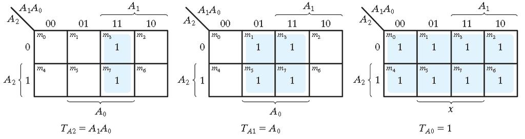
46 Synthesis using T Flip-flops NCNU_2016_DD_5_46 Example: n-bit binary counter consists of n flip-flops that can count in binary from 0 to 2 n - 1. The state diagram of a 3-bit counter is shown below, the input is the clock and the output is the state. A 2 A 1 A 0 3-bit Counter Clock
47 NCNU_2016_DD_5_47 Binary counters are constructed most efficiently with T flip-flops. Three flip-flops A 2, A 1, and A 0 are used. +
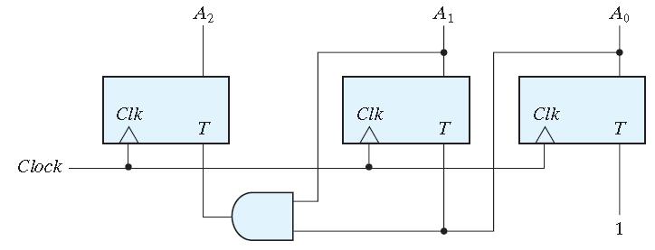
48 NCNU_2016_DD_5_48

49 NCNU_2016_DD_5_49 Flip-Flop Applications: Parallel Data Storage A group of flip-flops can store several bits of data from parallel lines simultaneously. Parallel data lines connected to the D inputs of flip-flops. All the clock inputs of the flip-flops are connected together, so that all the flip-flops are triggered by the same clock pulse. CLR is for asynchronous reset. It is a basic register, will be covered in the next chapter.


50 Flip-Flop Applications: Frequency Division NCNU_2016_DD_5_50 The D flip-flop and J-K flip-flop as a divide-by-2 device. Two D flip-flops used to divide the clock frequency by 4.

51 Flip-Flop Applications: Counting NCNU_2016_DD_5_51 Two J-K flip-flops used to generate a binary count sequence (00, 01, 10, 11).
 = xy + xb B(t + 1) = xa + xb z = A")
52 Homework #5 NCNU_2016_DD_5_ A sequential circuit with two D flip-flops A and B, two inputs, x and y ; and one output z is specified by the following next-state and output equations: A(t + 1) = xy + xb B(t + 1) = xa + xb z = A (a) Draw the logic diagram of the circuit. (b) List the state table for the sequential circuit. (c) Draw the corresponding state diagram. 5.8 Derive the state table and the state diagram of the sequential circuit shown below. Explain the function that the circuit performs.
53 NCNU_2016_DD_5_ A sequential circuit has two JK flip-flops A and B, two inputs x and y, and one output z. The flip-flop input equations and circuit output equation are JA = Bx + B y KA = B x + y JB = A x KB = A + xy z = (A + B)x y (a) Draw the logic diagram of the circuit. (b) Tabulate the state table. (c) Derive the state equations for A and B For the following state table (a) Draw the corresponding state diagram. (b) Tabulate the reduced state table. (c) Draw the state diagram corresponding to the reduced state table.
54 NCNU_2016_DD_5_ Design a sequential circuit with two D flip-flops A and B, and one input x_in. (a) When x_in = 0, the state of the circuit remains the same. When x_in = 1, the circuit goes through the state transitions from 00 to 01, to 11, to 10, back to 00, and repeats. (b) When x_in = 0, the state of the circuit remains the same. When x_in =1, the circuit goes through the state transitions from 00 to 11, to 01, to 10, back to 00, and repeats.
Digital Design, Kyung Hee Univ. Chapter 5. Synchronous Sequential Logic
 Chapter 5. Synchronous Sequential Logic 1 5.1 Introduction Electronic products: ability to send, receive, store, retrieve, and process information in binary format Dependence on past values of inputs Sequential
Sequential Circuits. Output depends only and immediately on the inputs Have no memory (dependence on past values of the inputs)
") Sequential Circuits Combinational circuits Output depends only and immediately on the inputs Have no memory (dependence on past values of the inputs) Sequential circuits Combination circuits with memory
Sequential Circuits Combinational circuits Output depends only and immediately on the inputs Have no memory (dependence on past values of the inputs) Sequential circuits Combination circuits with memory
Synchronous Sequential Logic. Chapter 5
 Synchronous Sequential Logic Chapter 5 5-1 Introduction Combinational circuits contains no memory elements the outputs depends on the inputs Synchronous Sequential Logic 5-2 5-2 Sequential Circuits Sequential
B.Tech CSE Sem. 3 15CS202 DIGITAL SYSTEM DESIGN (Regulations 2015) UNIT -IV
 UNIT -IV") B.Tech CSE Sem. 3 5CS22 DIGITAL SYSTEM DESIGN (Regulations 25) UNIT -IV SYNCHRONOUS SEQUENTIAL CIRCUITS OUTLINE FlipFlops SR,D,JK,T Analysis of Synchronous Sequential Circuit State Reduction and Assignment
B.Tech CSE Sem. 3 5CS22 DIGITAL SYSTEM DESIGN (Regulations 25) UNIT -IV SYNCHRONOUS SEQUENTIAL CIRCUITS OUTLINE FlipFlops SR,D,JK,T Analysis of Synchronous Sequential Circuit State Reduction and Assignment
Sequential Logic Circuits
 Sequential Logic Circuits By Dr. M. Hebaishy Digital Logic Design Ch- Rem.!) Types of Logic Circuits Combinational Logic Memoryless Outputs determined by current values of inputs Sequential Logic Has memory
Part II. Chapter2: Synchronous Sequential Logic
 課程名稱 : 數位系統設計導論 P-/77 Part II Chapter2: Synchronous Sequential Logic 教師 : 郭峻因教授 INSTRUCTOR: Prof. Jiun-In Guo E-mail: jiguo@cs.ccu.edu.tw 課程名稱 : 數位系統設計導論 P-2/77 Special thanks to Prof. CHING-LING SU for
Chapter 5 Synchronous Sequential Logic
 EEA051 - Digital Logic 數位邏輯 Chapter 5 Synchronous Sequential Logic 吳俊興國立高雄大學資訊工程學系 December 2005 Chapter 5 Synchronous Sequential Logic 5-1 Sequential Circuits 5-2 Latches 5-3 Flip-Flops 5-4 Analysis of
Synchronous Sequential Logic
 Synchronous Sequential Logic ( 范倫達 ), Ph. D. Department of Computer Science National Chiao Tung University Taiwan, R.O.C. Fall, 2012 ldvan@cs.nctu.edu.tw http://www.cs.nctu.edu.tw/~ldvan/ Outlines Sequential
UNIT III. Combinational Circuit- Block Diagram. Sequential Circuit- Block Diagram
 UNIT III INTRODUCTION In combinational logic circuits, the outputs at any instant of time depend only on the input signals present at that time. For a change in input, the output occurs immediately. Combinational
Digital Logic Design Sequential Circuits. Dr. Basem ElHalawany
 Digital Logic Design Sequential Circuits Dr. Basem ElHalawany Combinational vs Sequential inputs X Combinational Circuits outputs Z A combinational circuit: At any time, outputs depends only on inputs
Synchronous Sequential Logic
 Synchronous Sequential Logic ( 范倫達 ), Ph. D. Department of Computer Science National Chiao Tung University Taiwan, R.O.C. Fall, 2017 ldvan@cs.nctu.edu.tw http://www.cs.nctu.edu.tw/~ldvan/ Outlines Sequential
Chapter 5 Synchronous Sequential Logic
 Chapter 5 Synchronous Sequential Logic Chih-Tsun Huang ( 黃稚存 ) http://nthucad.cs.nthu.edu.tw/~cthuang/ Department of Computer Science National Tsing Hua University Outline Introduction Storage Elements:
Synchronous Sequential Logic
 Synchronous Sequential Logic -A Sequential Circuit consists of a combinational circuit to which storage elements are connected to form a feedback path. The storage elements are devices capable of storing
Synchronous Sequential Logic
 Synchronous Sequential Logic Ranga Rodrigo August 2, 2009 1 Behavioral Modeling Behavioral modeling represents digital circuits at a functional and algorithmic level. It is used mostly to describe sequential
Synchronous Sequential Logic
 MEC520 디지털공학 Synchronous Sequential Logic Jee-Hwan Ryu School of Mechanical Engineering Sequential Circuits Outputs are function of inputs and present states Present states are supplied by memory elements
Digital Logic Design I
 Digital Logic Design I Synchronous Sequential Logic Mustafa Kemal Uyguroğlu Sequential Circuits Asynchronous Inputs Combinational Circuit Memory Elements Outputs Synchronous Inputs Combinational Circuit
Unit 11. Latches and Flip-Flops
 Unit 11 Latches and Flip-Flops 1 Combinational Circuits A combinational circuit consists of logic gates whose outputs, at any time, are determined by combining the values of the inputs. For n input variables,
MC9211 Computer Organization
 MC9211 Computer Organization Unit 2 : Combinational and Sequential Circuits Lesson2 : Sequential Circuits (KSB) (MCA) (2009-12/ODD) (2009-10/1 A&B) Coverage Lesson2 Outlines the formal procedures for the
Chapter. Synchronous Sequential Circuits
 Chapter 5 Synchronous Sequential Circuits Logic Circuits- Review Logic Circuits 2 Combinational Circuits Consists of logic gates whose outputs are determined from the current combination of inputs. Performs
CHAPTER 4: Logic Circuits
 CHAPTER 4: Logic Circuits II. Sequential Circuits Combinational circuits o The outputs depend only on the current input values o It uses only logic gates, decoders, multiplexers, ALUs Sequential circuits
NH 67, Karur Trichy Highways, Puliyur C.F, Karur District UNIT-III SEQUENTIAL CIRCUITS
 NH 67, Karur Trichy Highways, Puliyur C.F, 639 114 Karur District DEPARTMENT OF ELETRONICS AND COMMUNICATION ENGINEERING COURSE NOTES SUBJECT: DIGITAL ELECTRONICS CLASS: II YEAR ECE SUBJECT CODE: EC2203
CHAPTER 4: Logic Circuits
 CHAPTER 4: Logic Circuits II. Sequential Circuits Combinational circuits o The outputs depend only on the current input values o It uses only logic gates, decoders, multiplexers, ALUs Sequential circuits
D Latch (Transparent Latch)
") D Latch (Transparent Latch) -One way to eliminate the undesirable condition of the indeterminate state in the SR latch is to ensure that inputs S and R are never equal to 1 at the same time. This is done
D Latch (Transparent Latch) -One way to eliminate the undesirable condition of the indeterminate state in the SR latch is to ensure that inputs S and R are never equal to 1 at the same time. This is done
ELCT201: DIGITAL LOGIC DESIGN
 ELCT201: DIGITAL LOGIC DESIGN Dr. Eng. Haitham Omran, haitham.omran@guc.edu.eg Dr. Eng. Wassim Alexan, wassim.joseph@guc.edu.eg Lecture 6 Following the slides of Dr. Ahmed H. Madian ذو الحجة 1438 ه Winter
Flip-Flops. Because of this the state of the latch may keep changing in circuits with feedback as long as the clock pulse remains active.
 Flip-Flops Objectives The objectives of this lesson are to study: 1. Latches versus Flip-Flops 2. Master-Slave Flip-Flops 3. Timing Analysis of Master-Slave Flip-Flops 4. Different Types of Master-Slave
The reduction in the number of flip-flops in a sequential circuit is referred to as the state-reduction problem.
 State Reduction The reduction in the number of flip-flops in a sequential circuit is referred to as the state-reduction problem. State-reduction algorithms are concerned with procedures for reducing the
Chapter 5 Synchronous Sequential Logic
 Chapter 5 Synchronous Sequential Logic Sequential Circuits Latches and Flip-Flops Analysis of Clocked Sequential Circuits HDL Optimization Design Procedure Sequential Circuits Various definitions Combinational
`COEN 312 DIGITAL SYSTEMS DESIGN - LECTURE NOTES Concordia University
 `OEN 32 IGITL SYSTEMS ESIGN - LETURE NOTES oncordia University hapter 5: Synchronous Sequential Logic NOTE: For more eamples and detailed description of the material in the lecture notes, please refer
Chapter 5 Sequential Circuits
 Logic and omputer Design Fundamentals hapter 5 Sequential ircuits Part 1 Storage Elements and Sequential ircuit Analysis harles Kime & Thomas Kaminski 2008 Pearson Education, Inc. (Hyperlinks are active
CHAPTER1: Digital Logic Circuits
 CS224: Computer Organization S.KHABET CHAPTER1: Digital Logic Circuits 1 Sequential Circuits Introduction Composed of a combinational circuit to which the memory elements are connected to form a feedback
Other Flip-Flops. Lecture 27 1
 Other Flip-Flops Other types of flip-flops can be constructed by using the D flip-flop and external logic. Two flip-flops less widely used in the design of digital systems are the JK and T flip-flops.
Combinational / Sequential Logic
 Digital Circuit Design and Language Combinational / Sequential Logic Chang, Ik Joon Kyunghee University Combinational Logic + The outputs are determined by the present inputs + Consist of input/output
The word digital implies information in computers is represented by variables that take a limited number of discrete values.
 Class Overview Cover hardware operation of digital computers. First, consider the various digital components used in the organization and design. Second, go through the necessary steps to design a basic
Lecture 11: Synchronous Sequential Logic
 Lecture 11: Synchronous Sequential Logic Syed M. Mahmud, Ph.D ECE Department Wayne State University Aby K George, ECE Department, Wayne State University Contents Characteristic equations Analysis of clocked
Chapter 5. Introduction
 Chapter 5 Synchronous Sequential Logic Chapter 5 Introduction Circuits require memory to store intermediate data Sequential circuits use a periodic signal to determine when to store values. A clock signal
Chapter 8 Sequential Circuits
 Philadelphia University Faculty of Information Technology Department of Computer Science Computer Logic Design By 1 Chapter 8 Sequential Circuits 1 Classification of Combinational Logic 3 Sequential circuits
ECE 25 Introduction to Digital Design. Chapter 5 Sequential Circuits ( ) Part 1 Storage Elements and Sequential Circuit Analysis
 Part 1 Storage Elements and Sequential Circuit Analysis") EE 25 Introduction to igital esign hapter 5 Sequential ircuits (5.1-5.4) Part 1 Storage Elements and Sequential ircuit Analysis Logic and omputer esign Fundamentals harles Kime & Thomas Kaminski 2008 Pearson
EE 25 Introduction to igital esign hapter 5 Sequential ircuits (5.1-5.4) Part 1 Storage Elements and Sequential ircuit Analysis Logic and omputer esign Fundamentals harles Kime & Thomas Kaminski 2008 Pearson
COE 202: Digital Logic Design Sequential Circuits Part 1. Dr. Ahmad Almulhem ahmadsm AT kfupm Phone: Office:
 COE 202: Digital Logic Design Sequential Circuits Part 1 Dr. Ahmad Almulhem Email: ahmadsm AT kfupm Phone: 860-7554 Office: 22-324 Objectives Sequential Circuits Memory Elements Latches Flip-Flops Combinational
NH 67, Karur Trichy Highways, Puliyur C.F, Karur District DEPARTMENT OF INFORMATION TECHNOLOGY CS 2202 DIGITAL PRINCIPLES AND SYSTEM DESIGN
 NH 67, Karur Trichy Highways, Puliyur C.F, 639 114 Karur District DEPARTMENT OF INFORMATION TECHNOLOGY CS 2202 DIGITAL PRINCIPLES AND SYSTEM DESIGN UNIT 4 SYNCHRONOUS SEQUENTIAL LOGIC Sequential circuits
Introduction to Sequential Circuits
 Introduction to Sequential Circuits COE 202 Digital Logic Design Dr. Muhamed Mudawar King Fahd University of Petroleum and Minerals Presentation Outline Introduction to Sequential Circuits Synchronous
Logic Design. Flip Flops, Registers and Counters
 Logic Design Flip Flops, Registers and Counters Introduction Combinational circuits: value of each output depends only on the values of inputs Sequential Circuits: values of outputs depend on inputs and
ELCT201: DIGITAL LOGIC DESIGN
 ELCT201: DIGITAL LOGIC DESIGN Dr. Eng. Haitham Omran, haitham.omran@guc.edu.eg Dr. Eng. Wassim Alexan, wassim.joseph@guc.edu.eg Lecture 7 Following the slides of Dr. Ahmed H. Madian محرم 1439 ه Winter
UNIT IV. Sequential circuit
 UNIT IV Sequential circuit Introduction In the previous session, we said that the output of a combinational circuit depends solely upon the input. The implication is that combinational circuits have no
Sequential Logic. E&CE 223 Digital Circuits and Systems (A. Kennings) Page 1
 Page 1") Sequential Logic E&CE 223 igital Circuits and Systems (A. Kennings) Page 1 Sequential Circuits Have considered only combinational circuits in which circuit outputs are determined entirely by current circuit
Sequential Logic E&CE 223 igital Circuits and Systems (A. Kennings) Page 1 Sequential Circuits Have considered only combinational circuits in which circuit outputs are determined entirely by current circuit
Chapter 6. Flip-Flops and Simple Flip-Flop Applications
 Chapter 6 Flip-Flops and Simple Flip-Flop Applications Basic bistable element It is a circuit having two stable conditions (states). It can be used to store binary symbols. J. C. Huang, 2004 Digital Logic
ELCT201: DIGITAL LOGIC DESIGN
 ELCT201: DIGITAL LOGIC DESIGN Dr. Eng. Haitham Omran, haitham.omran@guc.edu.eg Dr. Eng. Wassim Alexan, wassim.joseph@guc.edu.eg Lecture 8 Following the slides of Dr. Ahmed H. Madian محرم 1439 ه Winter
Unit 9 Latches and Flip-Flops. Dept. of Electrical and Computer Eng., NCTU 1
 Unit 9 Latches and Flip-Flops Dept. of Electrical and Computer Eng., NCTU 1 9.1 Introduction Dept. of Electrical and Computer Eng., NCTU 2 What is the characteristic of sequential circuits in contrast
CS T34-DIGITAL SYSTEM DESIGN Y2/S3
 UNIT III Sequential Logic: Latches versus Flip Flops SR, D, JK, Master Slave Flip Flops Excitation table Conversion of Flip flops Counters: Asynchronous, synchronous, decade, presettable Shift Registers:
Vignana Bharathi Institute of Technology UNIT 4 DLD
 DLD UNIT IV Synchronous Sequential Circuits, Latches, Flip-flops, analysis of clocked sequential circuits, Registers, Shift registers, Ripple counters, Synchronous counters, other counters. Asynchronous
RS flip-flop using NOR gate
 RS flip-flop using NOR gate Triggering and triggering methods Triggering : Applying train of pulses, to set or reset the memory cell is known as Triggering. Triggering methods:- There are basically two
Combinational vs Sequential
 Combinational vs Sequential inputs X Combinational Circuits outputs Z A combinational circuit: At any time, outputs depends only on inputs Changing inputs changes outputs No regard for previous inputs
Chapter 3 Unit Combinational
 EE 2: igital Logic ircuit esign r Radwan E Abdel-Aal, OE Logic and omputer esign Fundamentals hapter 3 Unit ombinational 4 Sequential Logic esign ircuits Part Implementation Technology and Logic esign
MODULE 3. Combinational & Sequential logic
 MODULE 3 Combinational & Sequential logic Combinational Logic Introduction Logic circuit may be classified into two categories. Combinational logic circuits 2. Sequential logic circuits A combinational
SEQUENTIAL LOGIC. Satish Chandra Assistant Professor Department of Physics P P N College, Kanpur
 SEQUENTIAL LOGIC Satish Chandra Assistant Professor Department of Physics P P N College, Kanpur www.satish0402.weebly.com OSCILLATORS Oscillators is an amplifier which derives its input from output. Oscillators
Introduction. NAND Gate Latch. Digital Logic Design 1 FLIP-FLOP. Digital Logic Design 1
 2007 Introduction BK TP.HCM FLIP-FLOP So far we have seen Combinational Logic The output(s) depends only on the current values of the input variables Here we will look at Sequential Logic circuits The
2 Sequential Circuits
 2 2.1 State Diagrams and General Form 0/0 1/0 Start State 0 /0 1/1 State 1 /1 0/1 State Diagram of a Change Detector ( Mealy-machine). The output Y assumes 1 whenever the input X has changed. Otherwise
Solution to Digital Logic )What is the magnitude comparator? Design a logic circuit for 4 bit magnitude comparator and explain it,
What is the magnitude comparator? Design a logic circuit for 4 bit magnitude comparator and explain it,") Solution to Digital Logic -2067 Solution to digital logic 2067 1.)What is the magnitude comparator? Design a logic circuit for 4 bit magnitude comparator and explain it, A Magnitude comparator is a combinational
Solution to Digital Logic -2067 Solution to digital logic 2067 1.)What is the magnitude comparator? Design a logic circuit for 4 bit magnitude comparator and explain it, A Magnitude comparator is a combinational
ECE 341. Lecture # 2
 ECE 341 Lecture # 2 Instructor: Zeshan Chishti zeshan@pdx.edu October 1, 2014 Portland State University Announcements Course website reminder: http://www.ece.pdx.edu/~zeshan/ece341.htm Homework 1: Will
IT T35 Digital system desigm y - ii /s - iii
 UNIT - III Sequential Logic I Sequential circuits: latches flip flops analysis of clocked sequential circuits state reduction and assignments Registers and Counters: Registers shift registers ripple counters
6. Sequential Logic Flip-Flops
 ection 6. equential Logic Flip-Flops Page of 5 6. equential Logic Flip-Flops ombinatorial components: their output values are computed entirely from their present input values. equential components: their
EMT 125 Digital Electronic Principles I CHAPTER 6 : FLIP-FLOP
 EMT 125 Digital Electronic Principles I CHAPTER 6 : FLIP-FLOP 1 Chapter Overview Latches Gated Latches Edge-triggered flip-flops Master-slave flip-flops Flip-flop operating characteristics Flip-flop applications
Chapter 3. Boolean Algebra and Digital Logic
 Chapter 3 Boolean Algebra and Digital Logic Chapter 3 Objectives Understand the relationship between Boolean logic and digital computer circuits. Learn how to design simple logic circuits. Understand how
Logic Design II (17.342) Spring Lecture Outline
 Spring Lecture Outline") Logic Design II (17.342) Spring 2012 Lecture Outline Class # 05 February 23, 2012 Dohn Bowden 1 Today s Lecture Analysis of Clocked Sequential Circuits Chapter 13 2 Course Admin 3 Administrative Admin
Logic Design II (17.342) Spring 2012 Lecture Outline Class # 05 February 23, 2012 Dohn Bowden 1 Today s Lecture Analysis of Clocked Sequential Circuits Chapter 13 2 Course Admin 3 Administrative Admin
Module -5 Sequential Logic Design
 Module -5 Sequential Logic Design 5.1. Motivation: In digital circuit theory, sequential logic is a type of logic circuit whose output depends not only on the present value of its input signals but on
Problems with D-Latch
 Problems with -Latch If changes while is true, the new value of will appear at the output. The latch is transparent. If the stored value can change state more than once during a single clock pulse, the
Final Exam review: chapter 4 and 5. Supplement 3 and 4
 Final Exam review: chapter 4 and 5. Supplement 3 and 4 1. A new type of synchronous flip-flop has the following characteristic table. Find the corresponding excitation table with don t cares used as much
The outputs are formed by a combinational logic function of the inputs to the circuit or the values stored in the flip-flops (or both).
.") 1 The outputs are formed by a combinational logic function of the inputs to the circuit or the values stored in the flip-flops (or both). The value that is stored in a flip-flop when the clock pulse occurs
1 The outputs are formed by a combinational logic function of the inputs to the circuit or the values stored in the flip-flops (or both). The value that is stored in a flip-flop when the clock pulse occurs
INTRODUCTION TO SEQUENTIAL CIRCUITS
 NOTE: Explanation Refer Class Notes Digital Circuits(15EECC203) INTRODUCTION TO SEQUENTIAL CIRCUITS by Nagaraj Vannal, Asst.Professor, School of Electronics Engineering, K.L.E. Technological University,
CPS311 Lecture: Sequential Circuits
 CPS311 Lecture: Sequential Circuits Last revised August 4, 2015 Objectives: 1. To introduce asynchronous and synchronous flip-flops (latches and pulsetriggered, plus asynchronous preset/clear) 2. To introduce
EE292: Fundamentals of ECE
 EE292: Fundamentals of ECE Fall 2012 TTh 10:00-11:15 SEB 1242 Lecture 23 121120 http://www.ee.unlv.edu/~b1morris/ee292/ 2 Outline Review Combinatorial Logic Sequential Logic 3 Combinatorial Logic Circuits
EET2411 DIGITAL ELECTRONICS
 5-8 Clocked D Flip-FlopFlop One data input. The output changes to the value of the input at either the positive going or negative going clock trigger. May be implemented with a J-K FF by tying the J input
 WWW.STUDENTSFOCUS.COM + Class Subject Code Subject Prepared By Lesson Plan for Time: Lesson. No 1.CONTENT LIST: Introduction to Unit III 2. SKILLS ADDRESSED: Listening I year, 02 sem CS6201 Digital Principles
Logic and Computer Design Fundamentals. Chapter 7. Registers and Counters
 Logic and Computer Design Fundamentals Chapter 7 Registers and Counters Registers Register a collection of binary storage elements In theory, a register is sequential logic which can be defined by a state
Chapter 11 Latches and Flip-Flops
 Chapter 11 Latches and Flip-Flops SKEE1223 igital Electronics Mun im/arif/izam FKE, Universiti Teknologi Malaysia ecember 8, 2015 Types of Logic Circuits Combinational logic: Output depends solely on the
Chapter 5 Sequential Circuits
 Logic and Computer Design Fundamentals Chapter 5 Sequential Circuits Part 2 Sequential Circuit Design Charles Kime & Thomas Kaminski 28 Pearson Education, Inc. (Hyperlinks are active in View Show mode)
Sequential Circuits: Latches & Flip-Flops
 Sequential Circuits: Latches & Flip-Flops Overview Storage Elements Latches SR, JK, D, and T Characteristic Tables, Characteristic Equations, Eecution Tables, and State Diagrams Standard Symbols Flip-Flops
Lecture 8: Sequential Logic
 Lecture 8: Sequential Logic Last lecture discussed how we can use digital electronics to do combinatorial logic we designed circuits that gave an immediate output when presented with a given set of inputs
More on Flip-Flops Digital Design and Computer Architecture: ARM Edition 2015 Chapter 3 <98> 98
 More on Flip-Flops Digital Design and Computer Architecture: ARM Edition 2015 Chapter 3 98 Review: Bit Storage SR latch S (set) Q R (reset) Level-sensitive SR latch S S1 C R R1 Q D C S R D latch Q
Department of CSIT. Class: B.SC Semester: II Year: 2013 Paper Title: Introduction to logics of Computer Max Marks: 30
 Department of CSIT Class: B.SC Semester: II Year: 2013 Paper Title: Introduction to logics of Computer Max Marks: 30 Section A: (All 10 questions compulsory) 10X1=10 Very Short Answer Questions: Write
ELE2120 Digital Circuits and Systems. Tutorial Note 7
 ELE2120 Digital Circuits and Systems Tutorial Note 7 Outline 1. Sequential Circuit 2. Gated SR Latch 3. Gated D-latch 4. Edge-Triggered D Flip-Flop 5. Asynchronous and Synchronous reset Sequential Circuit
CHAPTER 1 LATCHES & FLIP-FLOPS
 CHAPTER 1 LATCHES & FLIP-FLOPS 1 Outcome After learning this chapter, student should be able to; Recognize the difference between latches and flipflops Analyze the operation of the flip flop Draw the output
LATCHES & FLIP-FLOP. Chapter 7
 LATCHES & FLIP-FLOP Chapter 7 INTRODUCTION Latch and flip flops are categorized as bistable devices which have two stable states,called SET and RESET. They can retain either of this states indefinitely
UNIT-3: SEQUENTIAL LOGIC CIRCUITS
 UNIT-3: SEQUENTIAL LOGIC CIRCUITS STRUCTURE 3. Objectives 3. Introduction 3.2 Sequential Logic Circuits 3.2. NAND Latch 3.2.2 RS Flip-Flop 3.2.3 D Flip-Flop 3.2.4 JK Flip-Flop 3.2.5 Edge Triggered RS Flip-Flop
Experiment 8 Introduction to Latches and Flip-Flops and registers
 Experiment 8 Introduction to Latches and Flip-Flops and registers Introduction: The logic circuits that have been used until now were combinational logic circuits since the output of the device depends
RS flip-flop using NOR gate
 RS flip-flop using NOR gate Triggering and triggering methods Triggering : Applying train of pulses, to set or reset the memory cell is known as Triggering. Triggering methods:- There are basically two
CHAPTER 6 COUNTERS & REGISTERS
 CHAPTER 6 COUNTERS & REGISTERS 6.1 Asynchronous Counter 6.2 Synchronous Counter 6.3 State Machine 6.4 Basic Shift Register 6.5 Serial In/Serial Out Shift Register 6.6 Serial In/Parallel Out Shift Register
Objectives. Combinational logics Sequential logics Finite state machine Arithmetic circuits Datapath
 Objectives Combinational logics Sequential logics Finite state machine Arithmetic circuits Datapath In the previous chapters we have studied how to develop a specification from a given application, and
Sequential Digital Design. Laboratory Manual. Experiment #3. Flip Flop Storage Elements
 The Islamic University of Gaza Engineering Faculty Department of Computer Engineering Spring 2018 ECOM 2022 Khaleel I. Shaheen Sequential Digital Design Laboratory Manual Experiment #3 Flip Flop Storage
1. Convert the decimal number to binary, octal, and hexadecimal.
 1. Convert the decimal number 435.64 to binary, octal, and hexadecimal. 2. Part A. Convert the circuit below into NAND gates. Insert or remove inverters as necessary. Part B. What is the propagation delay
The basic logic gates are the inverter (or NOT gate), the AND gate, the OR gate and the exclusive-or gate (XOR). If you put an inverter in front of
, the AND gate, the OR gate and the exclusive-or gate (XOR). If you put an inverter in front of") 1 The basic logic gates are the inverter (or NOT gate), the AND gate, the OR gate and the exclusive-or gate (XOR). If you put an inverter in front of the AND gate, you get the NAND gate etc. 2 One of the
1 The basic logic gates are the inverter (or NOT gate), the AND gate, the OR gate and the exclusive-or gate (XOR). If you put an inverter in front of the AND gate, you get the NAND gate etc. 2 One of the
(CSC-3501) Lecture 7 (07 Feb 2008) Seung-Jong Park (Jay) CSC S.J. Park. Announcement
 Lecture 7 (07 Feb 2008) Seung-Jong Park (Jay) CSC S.J. Park. Announcement") Seung-Jong Park (Jay) http://www.csc.lsu.edu/~sjpark Computer Architecture (CSC-3501) Lecture 7 (07 Feb 2008) 1 Announcement 2 1 Combinational vs. Sequential Logic Combinational Logic Memoryless Outputs
Seung-Jong Park (Jay) http://www.csc.lsu.edu/~sjpark Computer Architecture (CSC-3501) Lecture 7 (07 Feb 2008) 1 Announcement 2 1 Combinational vs. Sequential Logic Combinational Logic Memoryless Outputs
Chapter 5 Flip-Flops and Related Devices
 Chapter 5 Flip-Flops and Related Devices Chapter 5 Objectives Selected areas covered in this chapter: Constructing/analyzing operation of latch flip-flops made from NAND or NOR gates. Differences of synchronous/asynchronous
Digital Circuit And Logic Design I. Lecture 8
 Digital Circuit And Logic Design I Lecture 8 Outline Sequential Logic Design Principles (1) 1. Introduction 2. Latch and Flip-flops 3. Clocked Synchronous State-Machine Analysis Panupong Sornkhom, 2005/2
Digital Circuit And Logic Design I
 Digital Circuit And Logic Design I Lecture 8 Outline Sequential Logic Design Principles (1) 1. Introduction 2. Latch and Flip-flops 3. Clocked Synchronous State-Machine Panupong Sornkhom, 2005/2 2 1 Sequential
Section 6.8 Synthesis of Sequential Logic Page 1 of 8
 Section 6.8 Synthesis of Sequential Logic Page of 8 6.8 Synthesis of Sequential Logic Steps:. Given a description (usually in words), develop the state diagram. 2. Convert the state diagram to a next-state
Computer Architecture and Organization
 A-1 Appendix A - Digital Logic Computer Architecture and Organization Miles Murdocca and Vincent Heuring Appendix A Digital Logic A-2 Appendix A - Digital Logic Chapter Contents A.1 Introduction A.2 Combinational
WEEK 10. Sequential Circuits: Analysis and Design. Page 1
 WEEK 10 Sequential Circuits: Analysis and Design Page 1 Analysis of Clocked (Synchronous) Sequential Circuits Now that we have flip-flops and the concept of memory in our circuit, we might want to determine
Engr354: Digital Logic Circuits
 Engr354: igital Circuits Chapter 7 Sequential Elements r. Curtis Nelson Sequential Elements In this chapter you will learn about: circuits that can store information; Basic cells, latches, and flip-flops;
CS8803: Advanced Digital Design for Embedded Hardware
 CS883: Advanced Digital Design for Embedded Hardware Lecture 4: Latches, Flip-Flops, and Sequential Circuits Instructor: Sung Kyu Lim (limsk@ece.gatech.edu) Website: http://users.ece.gatech.edu/limsk/course/cs883
Dr.Mohamed Elmahdy Winter 2015 Eng.Yasmin Mohamed. Problem Set 6. Analysis and Design of Clocked Sequential Circuits. Discussion: 7/11/ /11/2015
 Dr. Elmahdy Winter 2015 Problem Set 6 Analysis and Design of Clocked Sequential Circuits Discussion: 7/11/2015 17/11/2015 *Exercise 6-1: (Problem 5.10) A sequential circuit has two JK flip-flops A and