Chapter 9 MSI Logic Circuits
|
|
|
- Corey Terry
- 6 years ago
- Views:
Transcription
1 Chapter 9 MSI Logic Circuits
2 Chapter 9 Objectives Selected areas covered in this chapter: Analyzing/using decoders & encoders in circuits. Advantages and disadvantages of LEDs and LCDs. Observation/analysis techniques to troubleshoot digital circuits. Operation of multiplexers and demultiplexers in circuit applications. Comparing two binary numbers by using the magnitude comparator circuit. Function and operation of code converters. Precautions when connecting digital circuits using the data bus concept. Using HDL to implement MSI logic circuits equivalents.
3 Chapter 9 Digital systems obtain data and information continuously operated on in some manner: Decoding/encoding. Multiplexing/demultiplexing,. Comparison; Code conversion; Data busing. These and other operations have been facilitated by the availability of numerous ICs in the MSI (medium-scale-integration) category.
4 9-1 Decoders Decoders are used when an output or a group of outputs is to be activated only on the occurrence of a specific combination of input levels. Often provided by outputs of a counter or a register.
; all the other outputs are LOW.")
5 9-1 Decoders A decoder accepts a set of inputs that represents a binary number activating only the output that corresponds to the input number. For each of these input combinations, only one of the M outputs will be active (HIGH); all the other outputs are LOW. Many decoders are designed to produce active-low outputs, where only the selected output is LOW while all others are HIGH.
6 9-1 Decoders Circuitry for a decoder with three inputs and 8 outputs. It uses all AND gates, so outputs are active-high Output O 6 goes HIGH only when CBA = 6 10.
 outputs.")
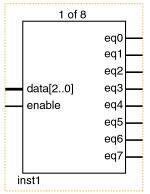
7 9-1 Decoders Circuitry for a decoder with three inputs and 8 outputs. This can be called a 3-line-to-8- line decoder it has three input lines and eight output lines. Also called a binary-to-octal decoder or converter taking three-bit binary input code and activating one of eight (octal) outputs. Also referred to as a 1-of-8 decoder only 1 of the 8 outputs is activated at one time.
8 9-1 Decoders Some decoders have one or more enable inputs used to control the operation of the decoder. The decoder is enabled only if ENABLE is HIGH. With common ENABLE line connected to a fourth input of each gate: If ENABLE is HIGH, the decoder functions normally. A, B, C input will determine which output is HIGH. If ENABLE is LOW, all outputs will be forced LOW. Regardless of the levels at the A, B, C inputs.


9 9-1 Decoders The 74ALS138 decoder. ENABLE inputs

10 9-1 Decoders 7442 BCD-to-decimal decoder. This decoder does not have an enable input.

11 9-1 Decoders 7445 BCD-to-decimal decoder/driver. Suitable for directly driving loads such as indicator LEDs or lamps, relays, or dc motors. Termed a driver because this IC has open-collector outputs that operate at higher current/voltage limits than a normal TTL output.
12 9-2 BCD-to-7 Segment Decoder/Drivers The 7-segment display is a common way to display decimal or hexadecimal characters. One common arrangement uses light emitting diodes (LEDs) for each segment. Diodes allow current to flow in one direction, but block flow in the other direction. When the LED anode is more positive than the cathode by approximately 2 V, the LED will light up.
13 9-2 BCD-to-7 Segment Decoder/Drivers The 7-segment display is a common way to display decimal or hexadecimal characters. One common arrangement uses light emitting diodes (LEDs) for each segment. By controlling current through each LED, some segments are turned on & emit light, while others are turned off, which generates the desired character pattern.

14 9-2 BCD-to-7 Segment Decoder/Drivers BCD-to-7-segment decoder/driver. The 7446/47 activates specific segment patterns in response to input codes
15 9-2 BCD-to-7 Segment Decoder/Drivers BCD-to-7-segment decoder/driver. This is a commonanode LED display. The anodes all of segments are tied together to V CC. Another type uses a common-cathode method, with each segment requiring 10 to 20 ma of current. TTL/CMOS devices are normally not used to drive a commoncathode display directly a transistor interface circuit is often used
16 9-3 Liquid Crystal Displays A liquid-crystal display (LCD) controls reflection of available light. The light may be ambient (room, sun) light. Reflective LCDs use ambient light. Available light might be provided by a small light source part of the display unit. Backlit LCDs use this method. LCDs have gained wide acceptance due to their very low power consumption compared to LEDs. LEDs have the advantage of a much brighter display that is easily visible in dark or poorly lit areas.
17 9-3 Liquid Crystal Displays Liquid-crystal display. Basic arrangement. Applying voltage between the segment and the backplane turns the segment ON. Zero voltage turns the segment OFF.

18 9-3 Liquid Crystal Displays Driving a 7- segment display. It is common to produce required ac voltage by applying out-of-phase square waves to the segment and the backplane.
19 9-3 Liquid Crystal Displays Liquid crystals are available as multidigit 7- segment decimal numeric displays. Alphanumeric LCD modules are available in many formats up to 4 lines by 40 characters. Other LCD modules allow the user to create a graphical display by controlling individual dots on the screen called pixels. Larger LCD panels can be scanned at a high rate, producing high quality video motion pictures. Control lines are arranged in rows & columns. A digital system must activate a matrix row/column to control the amount of light at each pixel.


20 9-3 Liquid Crystal Displays Each pixel on a color display is made up of three subpixels, which control light passing through a red, green, or blue filter to produce pixel color. A 640 x 480 LCD screen would have 640 x 3 connections for columns and 480 connections for rows a total of 2400 connections to the LCD.
21 9-3 Liquid Crystal Displays Older screens are called Twisted Nematic (TN) or Super Twisted Nematic (STN). Referred to as passive LCDs. Newer displays are called active matrix TFT LCDs. An active element on the display is used to switch pixels on and off. Other display technologies vacuum fluorescent, gas discharge plasma, and electroluminescence. Optical physics for each of these displays varies. The means of controlling all of them is the same.
22 9-4 Encoders 9-4 Encoders Most decoders accept an input code & produce a HIGH (or LOW) at one and only one output line. A decoder identifies, recognizes, or detects a particular code.

23 9-4 Encoders 9-4 Encoders The opposite of decoding process is encoding. Performed by a logic circuit called an encoder. An encoder has a number of input lines, only one of which is activated at a given time. Shown is an encoder with M inputs and N outputs. Inputs are active-high, which means that they are normally LOW. It produces an N-bit output code, depending on which input is activated.
24 9-4 Encoders An octal-to-binary encoder (8-line-to-3-line encoder) accepts eight input lines, producing a three-bit output code corresponding to the input. Logic circuit for an octal-to-binary (8-line-to-3-line) encoder. Only one input should be active at one time.

25 9-4 Encoders A priority encoder ensures that when two or more inputs are activated, the output code will correspond to the highest-numbered input. It has nine active-low inputs represent decimal digits 1 through 9, producing inverted BCD code corresponding to the highest-numbered activated input.
26 9-4 Encoders A switch encoder can be used when BCD data must be entered manually into a digital system. The 10 switches might be the keyboard switches on a calculator representing digits 0 through 9.

27 9-4 Encoders The switches are of the normally open type, so the encoder inputs are all normally HIGH. BCD output is When a key is depressed, the circuit will produce the BCD code for that digit. The 74LS147 is a priority encoder, so simultaneous key depressions produce the BCD code for the higher-numbered key.
28 9-5 Troubleshooting More complex circuitry increases possible reasons for failure Applying observation and analysis will narrow the focus and simplify testing After using observation and analysis to determine the possible faults, repeatedly use the divide and conquer technique to reduce possible causes by half.
29 9-6 Multiplexers (Data Selectors) A multiplexer (MUX) selects 1 of N input data sources and transmits the selected data to a single output called multiplexing. A digital multiplexer or data selector is a logic circuit that performs the same task. Routing control of desired data input to output by SELECT inputs referred to as ADDRESS inputs.
30 9-6 Multiplexers (Data Selectors) A two-input MUX could be used in a digital system that uses two different MASTER CLOCK signals. A high-speed clock in one mode and a slow-speed clock for the other.
31 9-6 Multiplexers (Data Selectors) Two-, four-, eight-, and 16-input multiplexers are available in the TTL and CMOS logic families. These basic ICs can be combined for multiplexing a larger number of inputs.
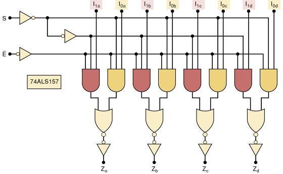
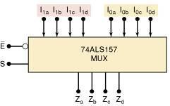
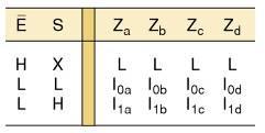
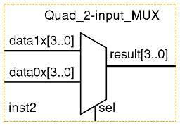
32 9-6 Multiplexers (Data Selectors) The 74ALS157 contains four two-input multiplexers
33 9-7 Multiplexer Applications Multiplexer circuits find numerous and varied applications in digital systems of all types. Data selection/routing, parallel-to-serial conversion. Operation sequencing. Waveform/logic-function generation.
34 9-7 Multiplexer Applications System for displaying two multidigit BCD counters one at a time.

35 9-7 Multiplexer Applications Parallel-to-serial converter. Waveforms for X 7 X 6 X 5 X 4 X 3 X 2 X 1 X

36 9-7 Multiplexer Applications Multiplexer used to implement a logic function described by the truth table.
37 9-8 Demultiplexers (Data Distributors) A demultiplexer (DEMUX) takes a single input and distributes it over several outputs. The select input code determines to which output the DATA input will be transmitted.
 A 1 line to 8 line")
38 9-8 Demultiplexers (Data Distributors) A 1 line to 8 line demultiplexer.

39 9-8 Demultiplexers (Data Distributors) Security monitoring system using the 74ALS138. The system shown can handle eight doors, but can be expanded to any number. The door switches are data inputs to the MUX. They produce a HIGH when a door is open and a LOW when it is closed.

40 9-8 Demultiplexers (Data Distributors) A synchronous data transmission system that is used to transmit four, four-bit words serially from a transmitter to a remote receiver.

41 9-8 Demultiplexers (Data Distributors) Synchronous data transmission system receiver block

42 9-8 Demultiplexers (Data Distributors) This timing diagram shows the parallel data loaded into the transmitter, the serial data stream, and distribution/storage of the four data values in the receiver registers.


43 9-9 More Troubleshooting Apply observation and analysis to this example: A test on the circuit yields the result shown. What is the probable circuit fault?


44 9-10 Magnitude Comparator Another useful MSI is a magnitude comparator. A combinational logic circuit that compares two input binary quantities and generates outputs to indicate which one has the greater magnitude. Megafunction symbol. Cascading inputs are not necessary on a megafunction simply specify larger data input ports.

45 9-10 Magnitude Comparator Another useful MSI is a magnitude comparator. A combinational logic circuit that compares two input binary quantities and generates outputs to indicate which one has the greater magnitude.

46 9-10 Magnitude Comparator Magnitude comparator used in a digital thermostat.

47 9-11 Code Converters A code converter is a logic circuit that changes data presented in one type of binary code to another type of binary code. Basic idea of a two-digit BCD-to-binary converter.
 to the next.")
48 9-11 Code Converters The bits in a BCD representation have decimal weights that are 8, 4, 2, 1 within each code group. That differ by a factor of 10 from one code group (decimal digit) to the next. The decimal weight of each bit in the BCD representation can be converted to its binary equivalent.
49 9-11 Code Converters One way to implement the logic circuit that performs conversion process is to use binary adder circuits.
50 9-12 Data Busing In computers, transfer of data takes place over a common set of connecting lines called a data bus. Devices tied to the data bus will often have tri-state outputs, or be tied to the data bus by tristate buffers. Devices commonly connected to a data bus: Microprocessors; Semiconductor memory chips. Digital-to-analog and analog-to-digital converters.

51 9-12 Data Busing Three different devices can transmit eight-bit data over an eight-line data bus to a microprocessor. Only one device at a time is enabled so bus contention is avoided.
52 9-13 The 74ALS173/HC173 Tristate Register The devices connected to a data bus will contain registers (usually flip-flops) that hold device data. Outputs of these registers are usually connected to tristate buffers allowing them to be tied to a data bus.
53 9-13 The 74ALS173/HC173 Tristate Register TTL 74ALS173 tristate register.

54 9-14 Data Bus Operation Tristate registers connected to a data bus. The contents of any one of the three registers can be paralleltransferred over the data bus to one of the other registers through proper application of logic levels to the register enable inputs.

55 9-14 Data Bus Operation The timing diagram shows various signals involved in the transfer of the data 1011 from register A to register C.

56 9-14 Data Bus Operation Simplified representation of bus arrangement. Simplified way to show signal activity on data bus lines.

57 9-14 Data Bus Operation Manufacturers have developed ICs that connect inputs & outputs internal to the chip. To reduce the number of IC pins & bus connections. Each I/O line will function as an input or an output depending on the states of the enable inputs bidirectional data lines.
58 END
MSI LOGIC CIRCUITS OUTLINE
 C A P T E R 9 MSI OGIC CIRCUITS OUTINE 9- Decoders 9-2 BCD-to-7-Segment Decoder/Drivers 9-3 iquid-crystal Displays 9-4 Encoders 9-5 Troubleshooting 9-6 Multiplexers (Data Selectors) 9-7 Multiplexer Applications
Data Sheet. Electronic displays
 Data Pack F Issued November 0 029629 Data Sheet Electronic displays Three types of display are available; each has differences as far as the display appearance, operation and electrical characteristics
Half-Adders. Ch.5 Summary. Chapter 5. Thomas L. Floyd
 Digital Fundamentals: A Systems Approach Functions of Combinational Logic Chapter 5 Half-Adders Basic rules of binary addition are performed by a half adder, which accepts two binary inputs (A and B) and
Contents Circuits... 1
 Contents Circuits... 1 Categories of Circuits... 1 Description of the operations of circuits... 2 Classification of Combinational Logic... 2 1. Adder... 3 2. Decoder:... 3 Memory Address Decoder... 5 Encoder...
FUNCTIONS OF COMBINATIONAL LOGIC
 FUNCTIONS OF COMBINATIONAL LOGIC Agenda Adders Comparators Decoders Encoders Multiplexers Demultiplexers Adders Basic Adders Adders are important in computers other types of digital systems in which numerical
MODULAR DIGITAL ELECTRONICS TRAINING SYSTEM
 MODULAR DIGITAL ELECTRONICS TRAINING SYSTEM MDETS UCTECH's Modular Digital Electronics Training System is a modular course covering the fundamentals, concepts, theory and applications of digital electronics.
NORTHWESTERN UNIVERSITY TECHNOLOGICAL INSTITUTE
 NORTHWESTERN UNIVERSITY TECHNOLOGICL INSTITUTE ECE 270 Experiment #8 DIGITL CIRCUITS Prelab 1. Draw the truth table for the S-R Flip-Flop as shown in the textbook. Draw the truth table for Figure 7. 2.
Engineering College. Electrical Engineering Department. Digital Electronics Lab
 Engineering College Electrical Engineering Department Digital Electronics Lab Prepared by: Dr. Samer Mayaleh Eng. Nuha Odeh 2009/2010-1 - CONTENTS Experiment Name Page 1- Measurement of Basic Logic Gates
Chapter 8 Functions of Combinational Logic
 ETEC 23 Programmable Logic Devices Chapter 8 Functions of Combinational Logic Shawnee State University Department of Industrial and Engineering Technologies Copyright 27 by Janna B. Gallaher Basic Adders
PHYSICS 5620 LAB 9 Basic Digital Circuits and Flip-Flops
 PHYSICS 5620 LAB 9 Basic Digital Circuits and Flip-Flops Objective Construct a two-bit binary decoder. Study multiplexers (MUX) and demultiplexers (DEMUX). Construct an RS flip-flop from discrete gates.
Chapter 2. Digital Circuits
 Chapter 2. Digital Circuits Logic gates Flip-flops FF registers IC registers Data bus Encoders/Decoders Multiplexers Troubleshooting digital circuits Most contents of this chapter were covered in 88-217
1 Hour Sample Test Papers: Sample Test Paper 1. Roll No.
 6.1.2 Sample Test Papers: Sample Test Paper 1 Roll No. Institute Name: Course Code: EJ/EN/ET/EX/EV/IC/IE/IS/MU/DE/ED/ET/IU Subject: Principles of Digital Techniques Marks: 25 1 Hour 1. All questions are
Bachelor Level/ First Year/ Second Semester/ Science Full Marks: 60 Computer Science and Information Technology (CSc. 151) Pass Marks: 24
 Pass Marks: 24") 2065 Computer Science and Information Technology (CSc. 151) Pass Marks: 24 Time: 3 hours. Candidates are required to give their answers in their own words as for as practicable. Attempt any TWO questions:
2065 Computer Science and Information Technology (CSc. 151) Pass Marks: 24 Time: 3 hours. Candidates are required to give their answers in their own words as for as practicable. Attempt any TWO questions:
Tribhuvan University Institute of Science and Technology Bachelor of Science in Computer Science and Information Technology
 Tribhuvan University Institute of Science and Technology Bachelor of Science in Computer Science and Information Technology Course Title: Digital Logic Full Marks: 60 + 0 + 0 Course No.: CSC Pass Marks:
EEE130 Digital Electronics I Lecture #1_2. Dr. Shahrel A. Suandi
 EEE130 Digital Electronics I Lecture #1_2 Dr. Shahrel A. Suandi 1-4 Overview of Basic Logic Functions Digital systems are generally built from combinations of NOT, AND and OR logic elements The combinations
SIGNETICS INTEGRATED CIRCUITS Low Power Schottky TTL 54LS00-74LS00 Series. Supply Current/typmA Delay/typns Quad 2-Input NAND Gate 54LS00/C,D
 SIGNETICS INTEGRATED CIRCUITS Low Power Schottky TTL 54LS00-74LS00 Series Rating Value Unit Voltage - V CC +7.0 V Input Voltage Range - V I -0.5 to +7.0 V Output Voltage - V out +5.5 V Operating Temperature
4.S-[F] SU-02 June All Syllabus Science Faculty B.Sc. II Yr. Instrumentation Practice [Sem.III & IV] S.Lot
![4.S-[F] SU-02 June All Syllabus Science Faculty B.Sc. II Yr. Instrumentation Practice [Sem.III & IV] S.Lot](/thumbs/90/103282534.jpg "4.S-[F] SU-02 June All Syllabus Science Faculty B.Sc. II Yr. Instrumentation Practice [Sem.III & IV] S.Lot") [Sem.III & IV] S.Lot. - 1 - [Sem.III & IV] S.Lot. - 2 - [Sem.III & IV] S.Lot. - 3 - Syllabus B.Sc. ( Instrumentation Practice ) Second Year ( Third and Forth Semester ) ( Effective from June 2014 ) [Sem.III
[Sem.III & IV] S.Lot. - 1 - [Sem.III & IV] S.Lot. - 2 - [Sem.III & IV] S.Lot. - 3 - Syllabus B.Sc. ( Instrumentation Practice ) Second Year ( Third and Forth Semester ) ( Effective from June 2014 ) [Sem.III
UNIT V 8051 Microcontroller based Systems Design
 UNIT V 8051 Microcontroller based Systems Design INTERFACING TO ALPHANUMERIC DISPLAYS Many microprocessor-controlled instruments and machines need to display letters of the alphabet and numbers. Light
1. Convert the decimal number to binary, octal, and hexadecimal.
 1. Convert the decimal number 435.64 to binary, octal, and hexadecimal. 2. Part A. Convert the circuit below into NAND gates. Insert or remove inverters as necessary. Part B. What is the propagation delay
MODULE 3. Combinational & Sequential logic
 MODULE 3 Combinational & Sequential logic Combinational Logic Introduction Logic circuit may be classified into two categories. Combinational logic circuits 2. Sequential logic circuits A combinational
DIGITAL CIRCUIT LOGIC UNIT 9: MULTIPLEXERS, DECODERS, AND PROGRAMMABLE LOGIC DEVICES
 DIGITAL CIRCUIT LOGIC UNIT 9: MULTIPLEXERS, DECODERS, AND PROGRAMMABLE LOGIC DEVICES 1 Learning Objectives 1. Explain the function of a multiplexer. Implement a multiplexer using gates. 2. Explain the
Logic Design Viva Question Bank Compiled By Channveer Patil
 Logic Design Viva Question Bank Compiled By Channveer Patil Title of the Practical: Verify the truth table of logic gates AND, OR, NOT, NAND and NOR gates/ Design Basic Gates Using NAND/NOR gates. Q.1
Chapter 7 Counters and Registers
 Chapter 7 Counters and Registers Chapter 7 Objectives Selected areas covered in this chapter: Operation & characteristics of synchronous and asynchronous counters. Analyzing and evaluating various types
DIGITAL FUNDAMENTALS
 DIGITAL FUNDAMENTALS A SYSTEMS APPROACH THOMAS L. FLOYD PEARSON Boston Columbus Indianapolis New York San Francisco Upper Saddle River Amsterdam Cape Town Dubai London Madrid Milan Munich Paris Montreal
DIGITAL SYSTEM DESIGN UNIT I (2 MARKS)
") DIGITAL SYSTEM DESIGN UNIT I (2 MARKS) 1. Convert Binary number (111101100) 2 to Octal equivalent. 2. Convert Binary (1101100010011011) 2 to Hexadecimal equivalent. 3. Simplify the following Boolean function
DIGITAL SYSTEM DESIGN UNIT I (2 MARKS) 1. Convert Binary number (111101100) 2 to Octal equivalent. 2. Convert Binary (1101100010011011) 2 to Hexadecimal equivalent. 3. Simplify the following Boolean function
DIGITAL SYSTEM FUNDAMENTALS (ECE421) DIGITAL ELECTRONICS FUNDAMENTAL (ECE422) COUNTERS
 DIGITAL ELECTRONICS FUNDAMENTAL (ECE422) COUNTERS") COURSE / CODE DIGITAL SYSTEM FUNDAMENTALS (ECE421) DIGITAL ELECTRONICS FUNDAMENTAL (ECE422) COUNTERS One common requirement in digital circuits is counting, both forward and backward. Digital clocks and
COURSE / CODE DIGITAL SYSTEM FUNDAMENTALS (ECE421) DIGITAL ELECTRONICS FUNDAMENTAL (ECE422) COUNTERS One common requirement in digital circuits is counting, both forward and backward. Digital clocks and
List of the CMOS 4000 series Dual tri-input NOR Gate and Inverter Quad 2-input NOR gate Dual 4-input NOR gate
 List of the CMOS 4000 series 4000 - Dual tri-input NOR Gate and Inverter 4001 - Quad 2-input NOR gate 4002 - Dual 4-input NOR gate 4006-18 stage Shift register 4007 - Dual Complementary Pair Plus Inverter
Semester 6 DIGITAL ELECTRONICS- core subject -10 Credit-4
 Semester 6 DIGITAL ELECTRONICS- core subject -10 Credit-4 Unit I Number system, Binary, decimal, octal, hexadecimal-conversion from one another-binary addition, subtraction, multiplication, division-binary
QUICK GUIDE COMPUTER LOGICAL ORGANIZATION - OVERVIEW
 QUICK GUIDE http://www.tutorialspoint.com/computer_logical_organization/computer_logical_organization_quick_guide.htm COMPUTER LOGICAL ORGANIZATION - OVERVIEW Copyright tutorialspoint.com In the modern
[2 credit course- 3 hours per week]
![[2 credit course- 3 hours per week]](/thumbs/94/121292011.jpg "[2 credit course- 3 hours per week]") Syllabus of Applied Electronics for F Y B Sc Semester- 1 (With effect from June 2012) PAPER I: Components and Devices [2 credit course- 3 hours per week] Unit- I : CIRCUIT THEORY [10 Hrs] Introduction;
Syllabus of Applied Electronics for F Y B Sc Semester- 1 (With effect from June 2012) PAPER I: Components and Devices [2 credit course- 3 hours per week] Unit- I : CIRCUIT THEORY [10 Hrs] Introduction;
TIME SCHEDULE. MODULE TOPICS PERIODS 1 Number system & Boolean algebra 17 Test I 1 2 Logic families &Combinational logic
 COURSE TITLE : DIGITAL INSTRUMENTS PRINCIPLE COURSE CODE : 3075 COURSE CATEGORY : B PERIODS/WEEK : 4 PERIODS/SEMESTER : 72 CREDITS : 4 TIME SCHEDULE MODULE TOPICS PERIODS 1 Number system & Boolean algebra
MUHAMMAD NAEEM LATIF MCS 3 RD SEMESTER KHANEWAL
 1. A stage in a shift register consists of (a) a latch (b) a flip-flop (c) a byte of storage (d) from bits of storage 2. To serially shift a byte of data into a shift register, there must be (a) one click
2. Counter Stages or Bits output bits least significant bit (LSB) most significant bit (MSB) 3. Frequency Division 4. Asynchronous Counters
 most significant bit (MSB) 3. Frequency Division 4. Asynchronous Counters") 2. Counter Stages or Bits The number of output bits of a counter is equal to the flip-flop stages of the counter. A MOD-2 n counter requires n stages or flip-flops in order to produce a count sequence
2. Counter Stages or Bits The number of output bits of a counter is equal to the flip-flop stages of the counter. A MOD-2 n counter requires n stages or flip-flops in order to produce a count sequence
EE Chip list. Page 1
 Chip # Description 7400 Quadruple 2-Input Positive NANDS 7401 Quadruple 2-Input Positive NAND with Open-Collector Outputs 7402 Quadruple 2-input Positive NOR 7403 Quadruple 2-Intput Positive NAND with
Solution to Digital Logic )What is the magnitude comparator? Design a logic circuit for 4 bit magnitude comparator and explain it,
What is the magnitude comparator? Design a logic circuit for 4 bit magnitude comparator and explain it,") Solution to Digital Logic -2067 Solution to digital logic 2067 1.)What is the magnitude comparator? Design a logic circuit for 4 bit magnitude comparator and explain it, A Magnitude comparator is a combinational
Solution to Digital Logic -2067 Solution to digital logic 2067 1.)What is the magnitude comparator? Design a logic circuit for 4 bit magnitude comparator and explain it, A Magnitude comparator is a combinational
CS302 Glossary. address : The location of a given storage cell or group of cells in a memory; a unique memory location containing one byte.
 CS302 Glossary ABEL Advanced Boolean Expression Language; a software compiler language for SPLD programming; a type of hardware description language (HDL) Adder A digital circuit which forms the sum and
Helping Material of CS302
 ABEL : Advanced Boolean Expression Language; a software compiler language for SPLD programming; a type of hardware description language (HDL) Adder : A digital circuit which forms the sum and carry of
TYPICAL QUESTIONS & ANSWERS
 DIGITALS ELECTRONICS TYPICAL QUESTIONS & ANSWERS OBJECTIVE TYPE QUESTIONS Each Question carries 2 marks. Choose correct or the best alternative in the following: Q.1 The NAND gate output will be low if
Minnesota State College Southeast
 ELEC 2211: Digital Electronics II A. COURSE DESCRIPTION Credits: 4 Lecture Hours/Week: 2 Lab Hours/Week: 4 OJT Hours/Week: *.* Prerequisites: None Corequisites: None MnTC Goals: None Minnesota State College
Integrated Circuits 7
 7 IC Test Clip Series For temporary connections to DIP package components Heavy-duty spring loaded hinge provides positive contact 20 AWG insulated gold contacts Color: white 22103 Part No. Product No.
Chapter 3: Sequential Logic Systems
 Chapter 3: Sequential Logic Systems 1. The S-R Latch Learning Objectives: At the end of this topic you should be able to: design a Set-Reset latch based on NAND gates; complete a sequential truth table
ME 515 Mechatronics. Introduction to Digital Electronics
 ME 55 Mechatronics /5/26 ME 55 Mechatronics Digital Electronics Asanga Ratnaweera Department of Faculty of Engineering University of Peradeniya Tel: 8239 (3627) Email: asangar@pdn.ac.lk Introduction to
Logic Devices for Interfacing, The 8085 MPU Lecture 4
 Logic Devices for Interfacing, The 8085 MPU Lecture 4 1 Logic Devices for Interfacing Tri-State devices Buffer Bidirectional Buffer Decoder Encoder D Flip Flop :Latch and Clocked 2 Tri-state Logic Outputs
Chapter 5 Flip-Flops and Related Devices
 Chapter 5 Flip-Flops and Related Devices Chapter 5 Objectives Selected areas covered in this chapter: Constructing/analyzing operation of latch flip-flops made from NAND or NOR gates. Differences of synchronous/asynchronous
ECE 372 Microcontroller Design
 E.g. Port A, Port B Used to interface with many devices Switches LEDs LCD Keypads Relays Stepper Motors Interface with digital IO requires us to connect the devices correctly and write code to interface
Experiment (6) 2- to 4 Decoder. Figure 8.1 Block Diagram of 2-to-4 Decoder 0 X X
 2- to 4 Decoder. Figure 8.1 Block Diagram of 2-to-4 Decoder 0 X X") 8. Objectives : Experiment (6) Decoders / Encoders To study the basic operation and design of both decoder and encoder circuits. To describe the concept of active low and active-high logic signals. To
8. Objectives : Experiment (6) Decoders / Encoders To study the basic operation and design of both decoder and encoder circuits. To describe the concept of active low and active-high logic signals. To
CS302 Digital Logic Design Solved Objective Midterm Papers For Preparation of Midterm Exam
 CS302 Digital Logic Design Solved Objective Midterm Papers For Preparation of Midterm Exam MIDTERM EXAMINATION Spring 2012 Question No: 1 ( Marks: 1 ) - Please choose one A SOP expression is equal to 1
UNIT 1: DIGITAL LOGICAL CIRCUITS What is Digital Computer? OR Explain the block diagram of digital computers.
 UNIT 1: DIGITAL LOGICAL CIRCUITS What is Digital Computer? OR Explain the block diagram of digital computers. Digital computer is a digital system that performs various computational tasks. The word DIGITAL
Date: Author: New: Revision: x SAULT COLLEGE OF APPLIED ARTS & TECHNOLOGY SAULT STE. MARIE, ONTARIO ELN TWO
 SAULT COLLEGE OF APPLIED ARTS & TECHNOLOGY SAULT STE. MARIE, ONTARIO COURSE OUTLINE Course Title: DIGITAL ELECTRONICS Code No.: ELN 107-5 Program: ELECTRICAL/ELECTRONIC TECHNICIAN Semester: TWO Date: AUGUST
CHAPTER1: Digital Logic Circuits
 CS224: Computer Organization S.KHABET CHAPTER1: Digital Logic Circuits 1 Sequential Circuits Introduction Composed of a combinational circuit to which the memory elements are connected to form a feedback
CCE RR REVISED & UN-REVISED KARNATAKA SECONDARY EDUCATION EXAMINATION BOARD, MALLESWARAM, BANGALORE G È.G È.G È..
 CCE RR REVISED & UN-REVISED O %lo ÆË v ÃO y Æ fio» flms ÿ,» fl Ê«fiÀ M, ÊMV fl 560 003 KARNATAKA SECONDARY EDUCATION EXAMINATION BOARD, MALLESWARAM, BANGALORE 560 003 G È.G È.G È.. Æ fioê, d È 2018 S.
Page No.1. CS302 Digital Logic & Design_ Muhammad Ishfaq
 Page No.1 File Version Update: (Dated: 17-May-2011) This version of file contains: Content of the Course (Done) FAQ updated version.(these must be read once because some very basic definition and question
Laboratory Objectives and outcomes for Digital Design Lab
 Class: SE Department of Information Technology Subject Logic Design Sem : III Course Objectives and outcomes for LD Course Objectives: Students will try to : COB1 Understand concept of various components.
PURBANCHAL UNIVERSITY
 [c] Implement a full adder circuit with a decoder and two OR gates. [4] III SEMESTER FINAL EXAMINATION-2006 Q. [4] [a] What is flip flop? Explain flip flop operating characteristics. [6] [b] Design and
16 Stage Bi-Directional LED Sequencer
 16 Stage Bi-Directional LED Sequencer The bi-directional sequencer uses a 4 bit binary up/down counter (CD4516) and two "1 of 8 line decoders" (74HC138 or 74HCT138) to generate the popular "Night Rider"
A Combined Combinational-Sequential System
 A Combined Combinational-Sequential System Object To construct a serial transmission circuit with a comparator to check the output. Parts () 7485 4-bit magnitude comparators (1) 74177 4-bit binary counter
TEST-3 (DIGITAL ELECTRONICS)-(EECTRONIC)
-(EECTRONIC)") 1 TEST-3 (DIGITAL ELECTRONICS)-(EECTRONIC) Q.1 The flip-flip circuit is. a) Unstable b) multistable c) Monostable d) bitable Q.2 A digital counter consists of a group of a) Flip-flop b) half adders c)
1 TEST-3 (DIGITAL ELECTRONICS)-(EECTRONIC) Q.1 The flip-flip circuit is. a) Unstable b) multistable c) Monostable d) bitable Q.2 A digital counter consists of a group of a) Flip-flop b) half adders c)
EXPERIMENT 8 Medium Scale Integration (MSI) Logic Circuits
 Logic Circuits") ELEC 00 Laboratory Manual Experiment 8 PRELAB Page of EXPERIMT 8 Medium Scale Integration (MSI) Logic Circuits Introduction In this lab you will learn to work with some simple MSI (medium scale integration)
ELEC 00 Laboratory Manual Experiment 8 PRELAB Page of EXPERIMT 8 Medium Scale Integration (MSI) Logic Circuits Introduction In this lab you will learn to work with some simple MSI (medium scale integration)
PHYS 3322 Modern Laboratory Methods I Digital Devices
 PHYS 3322 Modern Laboratory Methods I Digital Devices Purpose This experiment will introduce you to the basic operating principles of digital electronic devices. Background These circuits are called digital
Physics 217A LAB 4 Spring 2016 Shift Registers Tri-State Bus. Part I
 Physics 217A LAB 4 Spring 2016 Shift Registers Tri-State Bus Part I 0. In this part of the lab you investigate the 164 a serial-in, 8-bit-parallel-out, shift register. 1. Press in (near the LEDs) a 164.
VU Mobile Powered by S NO Group
 Question No: 1 ( Marks: 1 ) - Please choose one A 8-bit serial in / parallel out shift register contains the value 8, clock signal(s) will be required to shift the value completely out of the register.
Find the equivalent decimal value for the given value Other number system to decimal ( Sample)
") VELAMMAL COLLEGE OF ENGINEERING AND TECHNOLOGY, MADURAI 65 009 Department of Information Technology Model Exam-II-Question bank PART A (Answer for all Questions) (8 X = 6) K CO Marks Find the equivalent
VELAMMAL COLLEGE OF ENGINEERING AND TECHNOLOGY, MADURAI 65 009 Department of Information Technology Model Exam-II-Question bank PART A (Answer for all Questions) (8 X = 6) K CO Marks Find the equivalent
WINTER 15 EXAMINATION Model Answer
 Important Instructions to examiners: 1) The answers should be examined by key words and not as word-to-word as given in the model answer scheme. 2) The model answer and the answer written by candidate
Registers and Counters
 Registers and Counters Clocked sequential circuit = F/Fs and combinational gates Register Group of flip-flops (share a common clock and capable of storing one bit of information) Consist of a group of
Lab #10 Hexadecimal-to-Seven-Segment Decoder, 4-bit Adder-Subtractor and Shift Register. Fall 2017
 University of Texas at El Paso Electrical and Computer Engineering Department EE 2169 Laboratory for Digital Systems Design I Lab #10 Hexadecimal-to-Seven-Segment Decoder, 4-bit Adder-Subtractor and Shift
0 0/1 0/1 0/1 0/1 0/1 0/1 0/1 0/1 1 1 Stop bits. 11-bit Serial Data format
 Applications of Shift Registers The major application of a shift register is to convert between parallel and serial data. Shift registers are also used as keyboard encoders. The two applications of the
Operating Manual Ver.1.1
 Event Counter Operating Manual Ver.1.1 An ISO 9001 : 2000 company 94-101, Electronic Complex Pardesipura, Indore- 452010, India Tel : 91-731- 2570301/02, 4211100 Fax: 91-731- 2555643 e mail : info@scientech.bz
MAHARASHTRA STATE BOARD OF TECHNICAL EDUCATION (Autonomous)
") Subject Code: 17320 Model Answer Page 1 of 32 Important Instructions to examiners: 1) The answers should be examined by key words and not as word-to-word as given in the Model answer scheme. 2) The model
Subject Code: 17320 Model Answer Page 1 of 32 Important Instructions to examiners: 1) The answers should be examined by key words and not as word-to-word as given in the Model answer scheme. 2) The model
Analogue Versus Digital [5 M]
![Analogue Versus Digital [5 M]](/thumbs/93/111640168.jpg "Analogue Versus Digital [5 M]") Q.1 a. Analogue Versus Digital [5 M] There are two basic ways of representing the numerical values of the various physical quantities with which we constantly deal in our day-to-day lives. One of the ways,
Q.1 a. Analogue Versus Digital [5 M] There are two basic ways of representing the numerical values of the various physical quantities with which we constantly deal in our day-to-day lives. One of the ways,
AC103/AT103 ANALOG & DIGITAL ELECTRONICS JUN 2015
 Q.2 a. Draw and explain the V-I characteristics (forward and reverse biasing) of a pn junction. (8) Please refer Page No 14-17 I.J.Nagrath Electronic Devices and Circuits 5th Edition. b. Draw and explain
Bell. Program of Study. Accelerated Digital Electronics. Dave Bell TJHSST
 Program of Study Accelerated Digital Electronics TJHSST Dave Bell Course Selection Guide Description: Students learn the basics of digital electronics technology as they engineer a complex electronic system.
 UNIT 1 NUMBER SYSTEMS AND DIGITAL LOGIC FAMILIES 1. Briefly explain the stream lined method of converting binary to decimal number with example. 2. Give the Gray code for the binary number (111) 2. 3.
MAHARASHTRA STATE BOARD OF TECHNICAL EDUCATION (Autonomous) (ISO/IEC Certified) WINTER 2018 EXAMINATION MODEL ANSWER
 (ISO/IEC Certified) WINTER 2018 EXAMINATION MODEL ANSWER") Important Instructions to examiners: 1) The answers should be examined by key words and not as word-to-word as given in themodel answer scheme. 2) The model answer and the answer written by candidate may
Important Instructions to examiners: 1) The answers should be examined by key words and not as word-to-word as given in themodel answer scheme. 2) The model answer and the answer written by candidate may
VLSI Design: 3) Explain the various MOSFET Capacitances & their significance. 4) Draw a CMOS Inverter. Explain its transfer characteristics
 Explain the various MOSFET Capacitances & their significance. 4) Draw a CMOS Inverter. Explain its transfer characteristics") 1) Explain why & how a MOSFET works VLSI Design: 2) Draw Vds-Ids curve for a MOSFET. Now, show how this curve changes (a) with increasing Vgs (b) with increasing transistor width (c) considering Channel
1) Explain why & how a MOSFET works VLSI Design: 2) Draw Vds-Ids curve for a MOSFET. Now, show how this curve changes (a) with increasing Vgs (b) with increasing transistor width (c) considering Channel
7454 4x2 AND/NOR x4 AND/NOR x2 Ex-NOR/Ex-OR x NAND 2x INVERTER X8 OR/NOR 14. EXPANDER x4 AND EXPANDER 14
 NAND GATES 7400 4x2-Input 14 7401 4x2-Input 14 7403 4x2-Input 14 7410 3x3-Input 14 7412 3x3-Input 14 7420 2x4-Input 14 7422 2x4-Input 14 7426 4x2-Input 15V 14 7430 1x8-Input 14 74133 1x13-Input 16 74134
Theory Lecture Day Topic Practical Day. Week. number systems and their inter-conversion Decimal, Binary. 3rd. 1st. 1st
 Lesson Plan Name of the Faculty : Priyanka Nain Discipline: Electronics & Communication Engg. Semester:5th Subject:DEMP Lesson Plan Duration: 15 Weeks Work Load(Lecture/Practical) per week (In Hours):
MODU LE DAY. Class-A, B, AB and C amplifiers - basic concepts, power, efficiency Basic concepts of Feedback and Oscillation. Day 1
 DAY MODU LE TOPIC QUESTIONS Day 1 Day 2 Day 3 Day 4 I Class-A, B, AB and C amplifiers - basic concepts, power, efficiency Basic concepts of Feedback and Oscillation Phase Shift Wein Bridge oscillators.
Computer Systems Architecture
 Computer Systems Architecture Fundamentals Of Digital Logic 1 Our Goal Understand Fundamentals and basics Concepts How computers work at the lowest level Avoid whenever possible Complexity Implementation
Registers and Counters
 Registers and Counters Clocked sequential circuit = F/Fs and combinational gates Register Group of flip-flops (share a common clock and capable of storing one bit of information) Consist of a group of
LAB #6 State Machine, Decoder, Buffer/Driver and Seven Segment Display
 LAB #6 State Machine, Decoder, Buffer/Driver and Seven Segment Display LAB OBJECTIVES 1. Design a more complex state machine 2. Design a larger combination logic solution on a PLD 3. Integrate two designs
ID 421C: Designing with Segmented LCD Displays
 ID 421C: Designing with Segmented LCD Displays BNS Solutions Travis Weisberger Embedded Systems Engineer 13 October 2010 Version: 1.3 BNS Solutions A little something about BNS Engineering consulting firm
Lesson 12. Advanced Digital Integrated Circuits Flip-Flops, Counters, Decoders, Displays
 Lesson 12 Sierra College CIE-01 Jim Weir 530.272.2203 jweir43@gmail.com www.rstengineering.com/sierra Advanced Digital Integrated Circuits Flip-Flops, Counters, Decoders, Displays Flip-Flops: True name
VTU NOTES QUESTION PAPERS NEWS RESULTS FORUMS Registers
 Registers Registers are a very important digital building block. A data register is used to store binary information appearing at the output of an encoding matrix.shift registers are a type of sequential
Decade Counters Mod-5 counter: Decade Counter:
 Decade Counters We can design a decade counter using cascade of mod-5 and mod-2 counters. Mod-2 counter is just a single flip-flop with the two stable states as 0 and 1. Mod-5 counter: A typical mod-5
Sep 09, APPLICATION NOTE 1193 Electronic Displays Comparison
 Sep 09, 2002 APPLICATION NOTE 1193 Electronic s Comparison Abstract: This note compares advantages and disadvantages of Cathode Ray Tubes, Electro-Luminescent, Flip- Dot, Incandescent Light Bulbs, Liquid
DM Segment Decoder Driver Latch with Constant Current Source Outputs
 DM9368 7-Segment Decoder Driver Latch with Constant Current Source Outputs General Description The DM9368 is a 7-segment decoder driver incorporating input latches and constant current output circuits
Quiz #4 Thursday, April 25, 2002, 5:30-6:45 PM
 Last (family) name: First (given) name: Student I.D. #: Circle section: Hu Saluja Department of Electrical and Computer Engineering University of Wisconsin - Madison ECE/CS 352 Digital System Fundamentals
University of Illinois at Urbana-Champaign
 University of Illinois at Urbana-Champaign Digital Electronics Laboratory Physics Department Physics 40 Laboratory Experiment 3: CMOS Digital Logic. Introduction The purpose of this lab is to continue
Massachusetts Institute of Technology Department of Electrical Engineering and Computer Science
 Massachusetts Institute of Technology Department of Electrical Engineering and Computer Science 6.111 - Introductory Digital Systems Laboratory Project Resources Project resources are allocated on a per
Subject : EE6301 DIGITAL LOGIC CIRCUITS
 QUESTION BANK Programme : BE Subject : Semester / Branch : III/EEE UNIT 1 NUMBER SYSTEMS AND DIGITAL LOGIC FAMILIES Review of number systems, binary codes, error detection and correction codes (Parity
Digital Fundamentals: A Systems Approach
 Digital Fundamentals: A Systems Approach Counters Chapter 8 A System: Digital Clock Digital Clock: Counter Logic Diagram Digital Clock: Hours Counter & Decoders Finite State Machines Moore machine: One
Electrical and Telecommunications Engineering Technology_TCET3122/TC520. NEW YORK CITY COLLEGE OF TECHNOLOGY The City University of New York
 NEW YORK CITY COLLEGE OF TECHNOLOGY The City University of New York DEPARTMENT: SUBJECT CODE AND TITLE: COURSE DESCRIPTION: REQUIRED: Electrical and Telecommunications Engineering Technology TCET 3122/TC
DM Segment Decoder/Driver/Latch with Constant Current Source Outputs
 DM9368 7-Segment Decoder/Driver/Latch with Constant Current Source Outputs General Description The DM9368 is a 7-segment decoder driver incorporating input latches and constant current output circuits
IT T35 Digital system desigm y - ii /s - iii
 UNIT - III Sequential Logic I Sequential circuits: latches flip flops analysis of clocked sequential circuits state reduction and assignments Registers and Counters: Registers shift registers ripple counters
ระบบคอมพ วเตอร และการเช อมโยง Computer Systems and Interfacing บทท 1 พ นฐานด จ ตอล
 04-612-307 ระบบคอมพ วเตอร และการเช อมโยง Computer Systems and Interfacing บทท 1 พ นฐานด จ ตอล สาขาว ชาว ศวกรรมคอมพ วเตอร คณะว ศวกรรมศาสตร มหาว ทยาล ยเทคโนโลย ราชมงคลพระนคร Digital and Analog Quantities
ET398 LAB 4. Concurrent Statements, Selection and Process
 ET398 LAB 4 Concurrent Statements, Selection and Process Decoders/Multiplexers February 16, 2013 Tiffany Turner OBJECTIVE The objectives of this lab were for us to become more adept at creating VHDL code
DIGITAL ELECTRONICS MCQs
 DIGITAL ELECTRONICS MCQs 1. A 8-bit serial in / parallel out shift register contains the value 8, clock signal(s) will be required to shift the value completely out of the register. A. 1 B. 2 C. 4 D. 8
Digital Electronic Circuits Design & Laboratory Guideline
 D.2. Encoders Often we use diverse peripheral devices such as switches, numeric keypads and more in order to interface the analog world with the digital one and, along with the usage of these devices,
DM Segment Decoder/Driver/Latch with Constant Current Source Outputs
 7-Segment Decoder/Driver/Latch with Constant Current Source Outputs General Description The DM9368 is a 7-segment decoder driver incorporating input latches and constant current output circuits to drive
Laboratory 1 - Introduction to Digital Electronics and Lab Equipment (Logic Analyzers, Digital Oscilloscope, and FPGA-based Labkit)
") Massachusetts Institute of Technology Department of Electrical Engineering and Computer Science 6. - Introductory Digital Systems Laboratory (Spring 006) Laboratory - Introduction to Digital Electronics
Massachusetts Institute of Technology Department of Electrical Engineering and Computer Science 6. - Introductory Digital Systems Laboratory (Spring 006) Laboratory - Introduction to Digital Electronics