Quickly converts glass slides into high-definition digital data by high-speed scanning!
|
|
|
- Marcia Hall
- 6 years ago
- Views:
Transcription
1

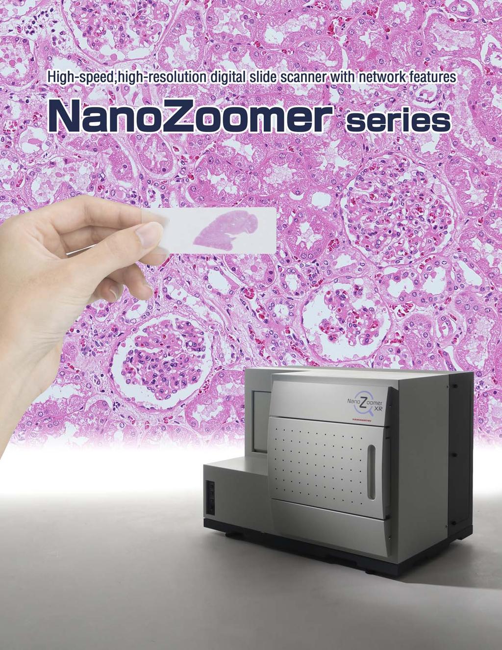
2 Quickly converts glass slides into high-definition digital data by high-speed scanning! Views the entire image of a sample and magnifies images to any size or detail just the same as by microscope observation. The NanoZoomer Series is a family of digital slide scanners that convert glass slides into high-resolution digital data by high-speed scanning. The NanoZoomer comes with a variety of functions such as image acquisition of fluorescence samples and multilayer acquisition. Scanned data can be viewed on a PC monitor by using the dedicated viewer software, and patented navigation map technique* delivers slide viewing environment just as if operating a microscope. *US Patent RE42,220E Digital slides have many advantages! Digitizing slides opens up a variety of new possibilities. Copying and Sharing Databases Digitized slides can be copied and shared. This feature of digital slides can be used in a variety of applications. For example, a large group of people can observe and discuss a single sample. Large numbers of digital slides can be stored into a database and incorporated into a laboratory information system. You can share data and construct slide libraries with distant facilities and research institutes. Slide Storage Digital data does not deteriorate, and it is more secure from damages and losses than glass slides. You can view digital data in its original quality anytime and anywhere. Networks Using the Internet or a local area network, you can observe and evaluate slides from a distant location. 2 * The NanoZoomer series as medical devices may be subject to government regulations where they are used. Hamamatsu makes no representation with regard to the conformity of these products to these regulations. Please consult your local Hamamatsu representative for more information.


 or 2 slides of double size (76 mm 52 mm) automatically. (The processing of double size slides is an optional feature.")
 to track and keep specimens in focus while scanning.")
3 High-end model NanoZoomer -XR Comes with rapid automatic processing of up to 320 slides, dynamic focus, and image quality judgment functions The NanoZoomer-XR is the next generation of digital slide scanners that delivers rapid yet high-quality scanning and also easy operation via automatic control. It quickly processes a huge volume of slides and the auto focus judgment function detects all types of scanning errors. Standard model NanoZoomer 2.0 -HT HT Automatic processing of up to 210 slides and a solid history of stable performance The NanoZoomer 2.0-HT is a user-friendly scanner designed to process up to 210 slides automatically. Just set the slides and press the start button, and all tasks from transferring the samples to acquiring their images are performed automatically. Since its launch on the market the NanoZoomer 2.0-HT has earned itself a high reputation from our many users. XR Compact model NanoZoomer 2.0 -RS RS Automatically process up to 6 slides of regular size or 2 slides of double size The NanoZoomer 2.0-RS is compact and affordable. It maintains the performance of the NanoZoomer 2.0-HT except for the number of slides processed automatically. It processes up to 6 slides of regular size (76 mm 26 mm) or 2 slides of double size (76 mm 52 mm) automatically. (The processing of double size slides is an optional feature.) Newly installed scan function XR This function delivers high-quality scanning along with smooth and easy operation. It is incorporated only into our top-end model - the NanoZoomer-XR. Sharp focus on entire specimen: Dynamic Pre-Focusing The NanoZoomer-XR uses its unique Dynamic Pre-Focusing Sample method (patent pending) to track and keep specimens in focus while scanning. It analyzes focus status right before capturing Glass slides an image and adjusts the objective lens to focus the image in real time. It keeps sharp focus on the entire specimen to generate high quality digital slides even from specimens which are difficult for the traditional focus mapping method. UP object lens object lens Analyze focus status Acquire focus image Focus status is analyzed right before imaging in real time. The focus status is used to control an objective lens in real time to acquire focused image. Free from time consuming manual slide quality check: Automatic focus scoring Manual slide quality check is often conducted after scanning to avoid scanning failure caused by dirt on a slide or sample folding. The NanoZoomer-XR evaluates scanned digital slides automatically and generates a focus score of each slide's quality for your review. Focus check points within a scanned slide are automatically determined, at each check point, focus is analyzed. Then a focus score is generated and displayed on a monitor screen. This score can be used for automated rescan. Optimized system condition whenever you scan: Automatic system calibration To maintain optimized condition of the scanner, routine calibrations of light intensity, white balance and shading are required. The NanoZoomer-XR automatically and periodically conducts a system calibration using a calibration slide located in a slide cassette, and keeps the system optimized. Whenever you scan, you will get the best digital slides it can deliver. Light intensity changes over time or due to environment temperature. Auto calibration 3


4 Digital slide scanner NanoZoomer series scan principle The scan units in the NanoZoomer Series employ "line scan" and "TDI mode" to scan sample tissues on glass slides at high speed and convert them into high-definition digital images. TDI mode line scan XR HT RS Variety of superior scan features from the expertise of Hamamatsu sensor technology. TDI combines both high speed and high sensitivity 3-chip TDI camera provides superior color reproduction The NanoZoomer series uses time delay integration (TDI) to provide high speed and high sensitivity simultaneously. Hamamatsu technology allows synchronizing TDI sensor signal with the movement of a microscopic sample object being scanned. The NanoZoomer series uses a 3-chip TDI camera to accurately reproduce sample colors. It enables observing minute variations in the colors of the sample. The 3-chip TDI camera has red, green and blue channels, and they are used to produce a single RGB image. Line scanning makes scanning faster Traditional CCD tiling Dedicated system design makes the NanoZoomer series user friendly and highly reliable. The NanoZoomer series is a specialized machine designed for routine use. It is user friendly and highly reliable. It employs a variety of sensors monitoring mechanical operations to ensure the safety of your slides. TDI Line Scanning Image composition Relatively slow scan and 2D composition of tiles Image composition The image is scanned line by line. Fast scanning and 1D composition Z-stack feature for thick samples There are samples which have 3D structures such as clumps of cells and thick tissues. They require focus adjustment during observation. To handle these kinds of slides, the NanoZoomer series is equipped with the Z-stack feature that allows you to focus on different depths in the sample. The NDP.view2 viewer software lets you adjust the focus on a Z-stack slide much like you would adjust the focus of a microscope. You can also point to an area of interest and let NDP.view2 apply autofocus for maximum clarity. X-axis Z-axis Y-axis +2.5 μm Unique TDI sensors realizes both high sensitivity and high speed simultaneously TDI sensor: Four steps (the actual NanoZoomer 2.0 sensors have 64 steps) The scanned object moves constantly, and the signal is reinforced at each stage by integrating the signal. This leads to fast and sensitive scanning. TDI sensor (Four steps) Signal level Depth direction μm μm μm μm μm ±0.00 μm 0.50 μm 1.00 μm 1.50 μm 2.00 μm 2.50 μm +1.5 μm 1st stage 2nd stage 3rd stage 4th stage -2.5 μm -1.5 μm ±0.0 μm 4

 Provision of Glass Slide Courtesy of Dr.")


.")


5 Examples Toxicity test using H&E staining NanoZoomer is available for a wide range of applications including toxicity evaluation. Liver in mouse with a dose of acetaminophen in 4 hours (Whole Image) Liver in mouse with a dose of acetaminophen in 4 hours (Magnified Image) Provision of Glass Slide Courtesy of Dr.June Kanno Division of Toxicology, Biological Safety Research Center, National Institute of Health Sciences, Japan Application for ips cells research Protein localization analysis using immunostaining NanoZoomer is great for testing ips cell differentiation ability by observation of teratoma tissue samples ranging from overall views to high-magnification images. NanoZoomer is ideal for observing localization of various types of proteins by using immunostaining techniques and so opens a host of diverse new applications. Teratoma formation by using mouse ips cells (HE-stain). Courtesy of Center for ips Research and Application, Kyoto University Specimen of needle biopsy stained by IHC(HER2) Courtesy of Dr.Kurozumi M, the Department of Pathology, Saitama Cancer Center, Japan Conferences using digital slides With digital slides, you can share the same sample among many people without worrying about sample deterioration. Observing H&E stained samples This is the basic staining method for tissue samples and is widely used for pathological examinations and tissue anatomy. PAS stained kidney biopsy sample Courtesy of Department of Pathology, The University of Tokyo Hospital, Hiroshi Uozaki, M.D., Ph.D. Pancreatic AVM with anisakiasis, resulting in pancreatic bleeding Courtesy of KobeCity Medical Center General Hospital, Department of Pathology, Yukihiro Imai, MD Ph.D. 5


6 Option Fluorescence imaging modules L12225 / L11600 Digitization of fluorescence samples enables long-term observation with no worries about fading, discoloration, or photobleaching. The Fluorescence Imaging Modules combined with the NanoZoomer Series are able to scan the entire image of fluorescence-stained samples at high speed and high resolution. The scanned images are saved as digital data which allows long-term observation without photobleaching which has been a difficult problem on conventional fluorescence microscopes. These modules also permit flexible observation of the overall sample image as well as the magnified or reduced images. The L and L /-22 come supplied with a filter wheel that automatically select and switches 6 filters for excitation and fluorescence wavelengths to sequentially acquire multiple fluorescence images. The L and L /-12 support fluorescence scanning in single, double and triple bands by simply replacing the filter cube. All models of the Fluorescence Imaging Modules use the L light source optimized for fluorescence microscopes that features high power, high stability, and long service life. NanoZoomer-XR + L /-02 Features of fluorescence imaging modules XR HT RS NanoZoomer 2.0-HT + L /-21 Adding a Fluorescence Imaging Module captures a diverse range of fluorescence images Scans samples stained with multiple fluorescence probes The Fluorescence Imaging Modules scan and generate digital data for samples stained with multiple fluorescence probes such as Q- dots, fluorochromes, fluorescence proteins, and others. The filter wheel unit automatically selects and switches 6 filters for excitation and fluorescence wavelengths to allow sequential image acquisition at single or multiple wavelengths. NanoZoomer 2.0-RS + L /-12/-21/-22 Uses dark field illumination for sample identification Superimposes images of entire tissues The Fluorescence Imaging Modules can superimpose a bright field image and a fluorescence image or superimpose two or more fluorescence images at tissue levels. This allows observing target protein localization and expression levels across the entire image. Uses high-power and long-life light source that needs no optical axis alignment The Fluorescence Imaging Modules use the L light source optimized for fluorescence microscopes. It offers an extremely long service life of 2000 hours as well as high power and high stability. No optical axis alignment is required even when the lamp is replaced. Fluorescence sample locations on a slide are usually difficult to find using transmitted illumination, so the Fluorescence Imaging Modules use dark field illumination * to pinpoint sample locations. This makes it easy to extract samples of interest. *Patent registered Features highly efficient optics ideal for TDI sensors To improve excitation light level density, the Fluorescence Imaging Modules efficiently condense a light flux onto the elongated area on a TDI line sensor that activates in transfer integration mode. This allows capturing even very weak fluorescence at high speed and also reduces the effect of photobleaching on samples since no excitation light is irradiated onto unwanted areas. Fluorescence module specifications Products number L L L L L L Applicable model XR XR HT/RS RS HT/RS RS Light source L *1 200W Ultrahigh-pressure mercury lamp Number of filter cubes installed* Filter wheel - 6Ex/6Em - - 6Ex/6Em 6Ex/6Em *1 See the table below for L specifications. *2 Filter cubes and filters are sold separately. Please consult us. 6 FL-illumination lamp unit L specification Dimensional outline / Weight Power consumption 180 mm(w) 299 mm(d) 227 mm(h) Approx. 6.8 kg 300 VA


7 Examples Rapid and High-Fidelity Imaging of Fluorescence-Labeled Q-dots Human pancreas Nucleus: Hoechst Chromogranin (endocrine gland, islets of Langerhans): Qdot655 Cytokeratin (exocrine gland): Qdot565 Courtesy of the Department of Pathology, Keio University School of Medicine Horizontal Section of the Nile Rat Brain Showing the Crossing of Retinal Axons in the Optic Chiasm Left eye was injected with Cholera Toxin B conjugated to Alexa 488; Right eye with Cholera Toxin B conjugated to Alexa 596. Images show the axon bundles as they cross to the opposite sides of the brain. Courtesy of the Harvey Karten, University of California-San Diego, USA; Yves Sauve, University of Alberta, Canada; Frederic Gaillard, Universite de Poitiers, Poitiers, France Observing multi-wavelength fluorescence image of TMA TMA images were acquired in the course of joint research with the National Cancer Center Research Institute, Department of Chemotherapy and Department of Pathology. 7
8 ERROR BUSY POWER Specifications Product name Product number Scanning method 20 mode (15 mm 15 mm) Scanning speeds 40 mode (15 mm 15 mm) Objective lens Scanning range Slide loader 20 mode Scanning resolution 40 mode Focusing method Z-stack feature Fluorescence imaging module Barcode reader Image compression Slide format Power supply voltage Power consumption NanoZoomer-XR C12000 Approx. 35 s Approx. 45 s 26 mm 76 mm Automatic, max. 320 slides Dynamic Pre-Focus Pre-Foucus map NanoZoomer 2.0-HT NanoZoomer 2.0-RS C9600 C10730 TDI (Time Delay Integration) Approx. 60 s Approx. 60 s Approx.150 s Approx. 150 s 20 (NA 0.75) User can select 20 or 40 mode at start of scanning. 26 mm 76 mm 26 mm 76 mm 52 mm 76 mm (Option) Automatic, max. 210 slides Standard size: 6 slides, Double size: 2 slides 0.46 μm 0.23 μm Pre-Foucus map Pre-Foucus map Acquires Z-stack images over entire scan area Option 1D barcode (standard feature), 2D barcode (option) JPEG compression JPEG compressed image + slide information AC 100 V to AC 240 V 300 VA 400 VA Dimensional outlines NanoZoomer-XR C12000 (Dedicated rack supplied as standard equipment) Weight Main unit: Approx.142 kg, Dedicated rack: Approx. 67 kg NanoZoomer 2.0-HT C9600 Weight Approx. 94 kg (Unit: mm) 636.5± ±5 738±3 623±5 860± ±3 731±3 NanoZoomer 2.0-RS C10730 Weight Approx. 72 kg 637±5 1000±5 660±5 540± ±5 * The NanoZoomer series as medical devices may be subject to government regulations where they are used. Hamamatsu makes no representation with regard to the conformity of these products to these regulations. Please consult your local sales representative for more information. NanoZoomer is a registered trademark of Hamamatsu Photonics K.K.. The university, institute, or company name of the researchers, whose measurement data is published in this brochure, is subject to change. Product and software package names noted in this documentation are trademarks or registered trademarks of their respective manufacturers. Subject to local technical requirements and regulations. Availability of products included in this promotional material may vary. Please consult with your local sales representative. Information furnished by HAMAMATSU is believed to be reliable. However, no responsibility is assumed for possible inaccuracies or omissions. Specifications and external appearance are subject to change without notice Hamamatsu Photonics K.K. HAMAMATSU PHOTONICS K.K. HAMAMATSU PHOTONICS K.K., Systems Division 812 Joko-cho, Higashi-ku, Hamamatsu City, , Japan, Telephone: (81) , Fax: (81) , export@sys.hpk.co.jp U.S.A.: Hamamatsu Corporation: 360 Foothill Road, Bridgewater, N.J 08807, U.S.A., Telephone: (1) , Fax: (1) usa@hamamatsu.com Germany: Hamamatsu Photonics Deutschland GmbH.: Arzbergerstr. 10, D Herrsching am Ammersee, Germany, Telephone: (49) , Fax: (49) info@hamamatsu.de France: Hamamatsu Photonics France S.A.R.L.: 19, Rue du Saule Trapu, Parc du Moulin de Massy, Massy Cedex, France, Telephone: (33) , Fax: (33) infos@hamamatsu.fr United Kingdom: Hamamatsu Photonics UK Limited: 2 Howard Court,10 Tewin Road, Welwyn Garden City, Hertfordshire AL7 1BW, UK, Telephone: (44) , Fax: (44) info@hamamatsu.co.uk North Europe: Hamamatsu Photonics Norden AB: Torshamnsgatan Kista, Sweden, Telephone: (46) , Fax: (46) info@hamamatsu.se Italy: Hamamatsu Photonics Italia S.r.l.: Strada della Moia, 1 int Arese (Milano), Italy, Telephone: (39) , Fax: (39) info@hamamatsu.it China: Hamamatsu Photonics (China) Co., Ltd.: B1201 Jiaming Center, No.27 Dongsanhuan Beilu, Chaoyang District, Beijing , China, Telephone: (86) , Fax: (86) hpc@hamamatsu.com.cn Cat. No. SBIS0043E04 MAR/2014 HPK Created in Japan
High-speed, high-resolution digital slide scanner with network features
 High-speed, high-resolution digital slide scanner with network features R NanoZoomer 2.0 series proposes new methods in drug development and medical research. The NanoZoomer 2.0 series is a system that
All-in-one solutions For applications with imaging challenges, we offer a wide range of TDI solutions.
 Speed Sensitivity Resolution All-in-one solutions For applications with imaging challenges, we offer a wide range of solutions. high-throughput Imaging in Low Light Applications New Generation of Solves
UV-LED MODULE. UV Irradiation Intensity Distribution Graphs
 UV-LED MODULE UV Irradiation Intensity Distribution Graphs Product Lineup Lens Lineup Product Lineup LED DRIVER C1559-1 LED HEAD UNIT L1561/L196 SERIES standard type standard type high power type high
Short wavelength type APD. Effective photosensitive area (mm) Effective photosensitive area size* 2
 Effective photosensitive area size* 2") Short wavelength type APD Features High sensitivity at visible range Low noise High gain Low capacitance Applications Low-light-level measurement Analytical instrument Structure / Absolute maximum ratings
Short wavelength type APD Features High sensitivity at visible range Low noise High gain Low capacitance Applications Low-light-level measurement Analytical instrument Structure / Absolute maximum ratings
Low bias operation, for 800 nm band
 Low bias operation, for 800 nm band These are 800 nm band near-infrared Si APDs that can operate at low voltages, 200 V or less. They are suitable for applications such as FSO (free space optics) and optical
Optics modules. Absorbance measurement module with built-in photodiode array, optical elements, current-tovoltage. C13398 series.
 Absorbance measurement module with built-in photodiode array, optical elements, current-tovoltage converter, etc. The is an optics module for absorbance measurement featuring high blocking performance
Photosensitive area size (mm) Reverse voltage VR max (V) R to +60
 Reverse voltage VR max (V) R to +60") ,, 6 to 37 mm resistance length PSD for precision distance measurement Hamamatsu provides various types of one-dimensional PSD (position sensitive detector) designed for precision distance measurement
,, 6 to 37 mm resistance length PSD for precision distance measurement Hamamatsu provides various types of one-dimensional PSD (position sensitive detector) designed for precision distance measurement
Application OCT. Dimensions (mm) Weight (g) Operating temperature* 1 Storage temperature* 1 λ=1.55 μm (V) (mw)
 Weight (g) Operating temperature* 1 Storage temperature* 1 λ=1.55 μm (V) (mw)") Balanced detectors with reduced multiple reflections These are differential amplification type photoelectric conversion modules containing two Hamamatsu photodiodes with balanced characteristics. The photodiodes
Balanced detectors with reduced multiple reflections These are differential amplification type photoelectric conversion modules containing two Hamamatsu photodiodes with balanced characteristics. The photodiodes
Effective photosensitive area. Photosensitive area size
 High performance, high reliability Si PIN photodiodes The is a high-speed Si PIN photodiode having high sensitivity over a wide spectral range from visible to near infrared light. The provides high performance
Photon counting module
 Photon counting module Fiber coupling type, low-light-level detection The is a photon counting module that can detect low-level light. It consists of a TE-cooled single pixel photon counter (SPPC), signal
Peak emission wavelength: 3.9 μm
 Peak emission wavelength: 3.9 μm The is a high-output mid-infrared LED with a 3.9 µm peak emission wavelength. It is a product that has been achieved using Hamamatsu unique crystal growth technology and
MPPC modules. MPPC array modules for very-low-level light detection, 16 ch analog output. C13368/C13369 series (Analog output type)
") MPPC modules C13368/C13369 series (Analog output type) MPPC array modules for very-low-level light detection, 16 ch analog output The C13368/C13369 series (analog output type) is an optical measurement
MPPC modules C13368/C13369 series (Analog output type) MPPC array modules for very-low-level light detection, 16 ch analog output The C13368/C13369 series (analog output type) is an optical measurement
Driver circuit for CCD linear image sensor
 For CCD image sensor (S11151-2048) The is a driver circuit designed for Hamamatsu CCD image sensor S11151-2048. The can be used in spectrometers when combined with the S11151-2048. The holds a CCD driver
Driver circuit for InGaAs linear image sensor
 (G11135 series, G14006-512DE) The is a driver circuit developed for InGaAs linear image sensors (G11135 series, G14006-512DE). The driver circuit consists of an analog video signal processing circuit (16-bit
InGaAs multichannel detector head
 Near infrared line camera (Line rate: 31.25 khz) The is a multichannel detector head suitable for applications where high-speed response is required, such as SD- OCT (spectral domain-optical coherence
InAsSb photovoltaic detector
 InAsSb photovoltaic detector P12691-21 High-speed response and high sensitivity in the 8 μm spectral band Thermoelectrically cooled infrared detector with no liquid nitrogen required The P12691-21 is an
Effective photosensitive area (mm)
") Chip carrier package for mount The, S5107, and S7510 are Si PIN photodiodes sealed in chip carrier packages suitable for mount using automated solder reflow techniques. These photodiodes have large photosensitive
Chip carrier package for mount The, S5107, and S7510 are Si PIN photodiodes sealed in chip carrier packages suitable for mount using automated solder reflow techniques. These photodiodes have large photosensitive
Effective photosensitive* 2 area size. Storage temperature Tstg (mm) ( C) ( C) S φ0.2 φ0.5 S φ to to +100 S9075
 ( C) ( C) S φ0.2 φ0.5 S φ to to +100 S9075") /-05/-10, S5344, S5345 Short wavelength type APD, for 600 nm band These are short wavelength APDs with improved sensitivity in the UV to visible range. They offer high gain, high sensitivity, and low noise
/-05/-10, S5344, S5345 Short wavelength type APD, for 600 nm band These are short wavelength APDs with improved sensitivity in the UV to visible range. They offer high gain, high sensitivity, and low noise
Driver circuit for InGaAs linear image sensor
 Driver circuit for InGaAs linear image sensor [G11620 series (non-cooled type)] The is a driver circuit developed for InGaAs linear image sensors [G11620 series (non-cooled type)]. The driver circuit consists
Effective photosensitive area (mm) Photosensitive area size
 Photosensitive area size") High UV resistance, photodiodes for UV monitor The are Si photodiodes that have achieved high reliability for monitoring ultraviolet light by employing a structure that does not use resin. They exhibit
High UV resistance, photodiodes for UV monitor The are Si photodiodes that have achieved high reliability for monitoring ultraviolet light by employing a structure that does not use resin. They exhibit
Parameter Symbol Specification Unit Photosensitive area - ɸ0.8 mm Package mm
 Surface mount type, high-speed Si photodiode The is a Si PIN photodiode with sensitivities in the visible to near infrared range and is compatible with lead-free solder reflow. It features high-speed response
Power supply for MPPC
 Power supply for MPPC C1104-0 Bias power supply with built-in high precision temperature compensation for MPPCs The C1104-0 is a high voltage power supply that is optimized for MPPCs (multi-pixel photon
Driver circuits for CCD image sensor
 Driver circuit for CCD image sensor (S10420/S11071/S11510 series) The and are driver circuits designed for HAMAMATSU CCD image sensor S10420/S11071/S11510 series. The and can be used in spectrometer when
Peak emission wavelength: 4.3 μm
 Peak emission wavelength: 4.3 μm The is a mid infrared LED with a 4.3 μm peak emission wavelength. It is a product that has been achieved using Hamamatsu unique crystal growth technology and process technology.
Driver circuit for CMOS linear image sensor
 Driver circuit for CMOS linear image sensor C13015-01 For CMOS linear image sensor S11639-01, etc. The C13015-01 is a driver circuit developed for Hamamatsu CMOS linear image sensor S11639-01, etc. By
InAsSb photovoltaic detectors
 High-speed response and high sensitivity in the spectral band up to 11 μm Infrared detectors The are photovoltaic type infrared detectors that have achieved high sensitivity in the spectral band up to
Accessories for infrared detector
 Temperature controllers Heatsinks for TE-cooled detector Chopper, etc. Wide lineups of accessories for infrared detector HAMAMATSU provides temperature controllers, heatsinks for TE-cooled detector, chopper
Peak sensitivity wavelength λp (nm) Photosensitive area (mm)
 Photosensitive area (mm)") Integrates a -PSD for precision photometry or a 4-segment Si photodiode with low-noise amp in a compact case PSD modules contain a high-precision two-dimensional PSD (position sensitive detector) or a
Integrates a -PSD for precision photometry or a 4-segment Si photodiode with low-noise amp in a compact case PSD modules contain a high-precision two-dimensional PSD (position sensitive detector) or a
Driver circuit for CCD linear image sensor
 Driver circuit for CCD linear image sensor C11165-02 For CCD image sensor (S11155/S11156-2048-02) The C11165-02 is a driver circuit designed for Hamamatsu CCD image sensor S11155/S11156-2048-02. The C11165-02
MPPC (Multi-Pixel Photon Counter)
") S13362-35DG Significantly reduced crosstalk, low afterpulses The can reduce dark count by cooling in addition to low afterpulses and low crosstalk of the S1336 series. The integrates the S1336 series with
S13362-35DG Significantly reduced crosstalk, low afterpulses The can reduce dark count by cooling in addition to low afterpulses and low crosstalk of the S1336 series. The integrates the S1336 series with
Signal processing circuit for 2-D PSD
 Signal processing circuit for 2-D PSD Circuit board for easier 2-D PSD operation The is a DC signal processing circuit for two-dimensional PSD. It is suitable for displacement measurements using DC light.
MPPC (multi-pixel photon counter)
") MPPC (multi-pixel photon counter) Low afterpulses, wide dynamic range, for high-speed measurement Photosensitive area: 1 1 mm These MPPCs utilize very small pixels arrayed at high densities to achieve
MPPC (multi-pixel photon counter) Low afterpulses, wide dynamic range, for high-speed measurement Photosensitive area: 1 1 mm These MPPCs utilize very small pixels arrayed at high densities to achieve
Signal processing circuit for 1-D PSD
 Signal processing circuit for 1-D PSD Circuit board for easier 1-D PSD operation The is a DC signal processing circuit for one-dimensional PSD. It is suitable for displacement measurements using DC light.
Driver circuit for MPPC
 Simple evaluation starter kit for non-cooled s The is a starter kit designed for simple non-cooled evaluations. It consists of a sensor board and a power supply board. The sensor board includes an socket
RGB color sensor. Effective photosensitive area. Green, Red: 2.25 Blue : 4.5
 Si photodiodes S6428-01 S6429-01 S6430-01 RGB color sensor The S6428-01, S6429-01 and S6430-01 are color sensors designed to respectively detect monochromatic colors of blue (λp=460 nm), green (λp=540
These Si photodiodes have sensitivity in the UV to near IR range. They are suitable for low-light-level detection in analysis and the like.
 UV to near IR for precision photometry These Si photodiodes have sensitivity in the UV to near IR range. They are suitable for low-light-level detection in analysis and the like. Features High sensitivity
Si PIN photodiodes. High-speed detectors with plastic package. Structure. Absolute maximum ratings
 High-speed detectors with plastic package The and are high-speed APC (auto power control) detectors developed for monitoring laser diodes with a peak wavelength of 66 nm or 78 nm. The is designed for surface
Infrared detector modules with preamp
 Easy-to-use detector modules with built-in preamps Infrared detector modules operate just by connecting to DC power supplies. The detector element is selectable from among InGaAs, InAs, InSb, and InAsSb
Parameter Specification Unit Photosensitive area mm Package Glass epoxy - Seal material Silicone resin -
 COB type, applicable to lead-free solder reflow The is a for visible to near infrared range and is compatible with lead-free solder reflow processes. The small and thin leadless package allows reducing
Photosensitive area (mm) 4 4. Peak sensitivity wavelength (nm) Supply voltage Dark state. Max. Vcc max. Tstg Min. Max. (ma) (V)
 4 4. Peak sensitivity wavelength (nm) Supply voltage Dark state. Max. Vcc max. Tstg Min. Max. (ma) (V)") Integrates a PSD for precision photometry or a 4-segment Si photodiode with low-noise amp in a compact case PSD modules contain a high-precision two-dimensional PSD (position sensitive detector) or a 4-segment
Integrates a PSD for precision photometry or a 4-segment Si photodiode with low-noise amp in a compact case PSD modules contain a high-precision two-dimensional PSD (position sensitive detector) or a 4-segment
Photo IC diode. Plastic package shaped the same as metal package. S SB. Features. Applications
 Plastic package shaped the same as metal package The photo IC has spectral response close to human eye sensitivity. Two photosensitive areas are made on a single chip. Almost only the visible range can
Si PIN photodiodes. High-speed detectors with plastic package. Structure. Absolute maximum ratings
 High-speed detectors with plastic package The and are high-speed APC (auto power control) detectors developed for monitoring laser diodes with a peak wavelength of 66 nm or 78 nm. The is designed for surface
Power supply for MPPC
 Power supply for MPPC C1104-0 Bias power supply with built-in high precision temperature compensation for MPPCs The C1104-0 is a high voltage power supply that is optimized for MPPCs (multi-pixel photon
APD modules. Operates an APD with single 5 V supply (standard type, short-wavelength type) C12702 series.
 C12702 series.") Operates an APD with single 5 V supply (standard type, short-wavelength type) Features Includes a high-sensitivity APD Uses a Hamamatsu high-sensitivity Si APD. Four types are available with different
Operates an APD with single 5 V supply (standard type, short-wavelength type) Features Includes a high-sensitivity APD Uses a Hamamatsu high-sensitivity Si APD. Four types are available with different
APD modules. APD module integrated with peripheral circuits. C12703 series. Selection guide. Block diagram
 APD module integrated with peripheral circuits Features Uses a high sensitivity APD Two types of APDs with different photosensitive areas (φ1.5 mm, φ3. mm) are provided. On-board high sensitivity circuit
Photosensor with front-end IC
 Compact APD suitable for various light level detection The is a compact optical device that integrates a Si APD and preamp. It has a built-in DC feedback circuit for reducing the effects of background
M=100, RL=50 Ω λ=800 nm, -3 db
 Low bias operation, for 800 nm band, small package Features Miniature and thin package:.8 3..0 t mm Stable operation at low bias High-speed response High sensitivity Low noise Applications Optical rangefinder
Reverse voltage VR max. Electrical and optical characteristics (Typ. Ta=25 C, unless otherwise noted) Short. Temp. S coefficient (A/W) of
 Short. Temp. S coefficient (A/W) of") Ceramic package photodiodes with low dark current The are ceramic package photodiodes that offer low dark current. Ceramic package used is light-impervious, so no stray light can reach the photosensitive
Ceramic package photodiodes with low dark current The are ceramic package photodiodes that offer low dark current. Ceramic package used is light-impervious, so no stray light can reach the photosensitive
Signal processing circuit for 2-D PSD
 Signal processing circuit for 2-D PSD Circuit board for easier 2-D PSD operation The is a DC signal processing circuit for two-dimensional PSD. It is suitable for displacement measurements using DC light.
Driver circuit for CMOS linear image sensor
 High-precision driver circuit with variable integration time function The is a driver circuit specifically designed for the Hamamatsu S10111 to S10114 series, S10121 to S10124 series (-01) current-output
Signal processing circuit for 1-D PSD
 Signal processing circuit for 1-D PSD Circuit board for easier 1-D PSD operation The is a DC signal processing circuit for one-dimensional PSD. It is suitable for displacement measurements using DC light.
16-element Si photodiode arrays
 Back-illuminated photodiode arrays for X-ray nondestructive inspection (element pitch: mm) The is a back-illuminated type 16-element photodiode array specifically designed for non-destructive X- ray inspection.
Suppressed IR sensitivity
 For UV to visible, precision photometry; suppressed IR sensitivity These Si photodiodes have suppressed IR sensitivity. They are suitable for low-light-level detection in analysis and the like. Features
16-element Si photodiode arrays
 Back-illuminated photodiode arrays for X-ray nondestructive inspection (element pitch: mm) The is a back-illuminated type 16-element photodiode array specifically designed for non-destructive X-ray inspection.
Driver circuit for CCD linear image sensor
 Driver circuit for CCD linear image sensor C11165-01 For CCD image sensor (S11155/S11156-2048-01) The C11165-01 is a driver circuit designed for HAMAMATSU CCD image sensor S11155/S11156-2048-01. The C11165-01
InAsSb photovoltaic detector
 InAsSb photovoltaic detector P2-2 High-speed response and high sensitivity in the 5 μm spectral band Thermoelectrically cooled infrared detector with no liquid nitrogen required The P2-2 is an infrared
PbSe photoconductive detectors
 PbSe photoconductive detectors P9696 series P327-8 Infrared detectors with fast response and high sensitivity in 5 μm wavelength band Compared to other detectors used in the same wavelength regions, PbSe
Si photodiode. Applicable to lead-free solder reflow and wide temperature range. S9674. Absolute maximum ratings
 Applicable to lead-free solder reflow and wide temperature range The is a photodiode that is applicable to lead-free solder reflow and has an extremely wide operating and storage temperature range (-40
1-D PSD with small plastic package
 1D PSD with small plastic package Hamamatsu offers a variety of 1D PSDs (position sensitive detectors) molded into plastic packages. These PSDs feature excellent position detection resolution, high resistance
Photo IC diode. Plastic package shaped the same as metal package. S SB. Absolute maximum ratings (Ta=25 C)
") Plastic package shaped the same as metal package The photo IC has spectral response close to human eye sensitivity. Two photosensitive areas are made on a single chip. Almost only the visible range can
Plastic package shaped the same as metal package The photo IC has spectral response close to human eye sensitivity. Two photosensitive areas are made on a single chip. Almost only the visible range can
InGaAs PIN photodiode arrays
 16/32/46 element InGaAs array for near IR detection The is one-dimensional InGaAs PIN photodiode array in a ceramic DIP (dual inline package). It can be used to perform simple spectroscopic analysis. Features
New product of near infrared (to 900 nm) detection
 detection") WITH THERMOELECTRIC COOLER H7844 New product of near infrared (to 900 nm) detection FEATURES A newly developed high sensitivity multialkali side-on photomultiplier tube Fast cooling (3 minutes) by thermoelectric
WITH THERMOELECTRIC COOLER H7844 New product of near infrared (to 900 nm) detection FEATURES A newly developed high sensitivity multialkali side-on photomultiplier tube Fast cooling (3 minutes) by thermoelectric
NMOS linear image sensor
 Image sensor highly sensitive to X-rays from 0 k to 00 kev s are self-scanning photodiode arrays designed specifically as detectors for multichannel spectroscopy. The scanning circuit is made up of N-channel
InAsSb photovoltaic detectors
 High-speed response and high sensitivity in the spectral band up to 5 μm Infrared detectors The are photovoltaic type infrared detectors that have achieved high sensitivity in the spectral band up to 5
16-element Si photodiode arrays
 S11212-421 S11212-321 S11212-021 S11212-121 Back-illuminated photodiode arrays for non-destructive inspection The is a back-illuminated type 16-element photodiode array specifically designed for non-destructive
Parameter Specification Unit Photosensitive area mm Package Glass epoxy - Seal material Epoxy resin -
 COB type, applicable to lead-free solder reflow The is a Si PIN photodiode for visible to near infrared range and is compatible with lead-free solder reflow processes. The small and thin leadless package
Photo IC diode. Wide operating temperature: -40 to +105 C. S MT. Absolute maximum ratings (Ta=25 C)
") Wide operating temperature: -40 to +05 C The photo IC has a spectral response close to human eye sensitivity. Two active areas are made on a single chip. Almost only the visible range can be measured by
Wide operating temperature: -40 to +05 C The photo IC has a spectral response close to human eye sensitivity. Two active areas are made on a single chip. Almost only the visible range can be measured by
Applications. Photosensitive area size. Storage temperature Tstg (mm) (mm 2 ) (V) ( C) ( C) S
 (mm 2 ) (V) ( C) ( C) S") , etc. Photodiodes molded into clear plastic packages These are Si photodiodes molded into clear plastic packages. Two types are available with sensitivity in the visible range and in the visible to near
, etc. Photodiodes molded into clear plastic packages These are Si photodiodes molded into clear plastic packages. Two types are available with sensitivity in the visible range and in the visible to near
Photodiode modules. C10439 series. Integrates photodiode for precision photometry with low-noise amp.
 Integrates photodiode for precision photometry with low-noise amp The photodiode modules are high-precision photodetectors that integrate a photodiode and a current-to-voltage amplifier. The output from
Non-discrete position sensors utilizing photodiode surface resistance
 Twodimensional PSD Nondiscrete position sensors utilizing photodiode surface resistance PSD (position sensitive detector) is an optoelectronic position sensor utilizing photodiode surface resistance. Unlike
MCT photoconductive detectors
 Non-cooled type and suitable for long, continuous operation Features Choice of spectral response (up to 12 μm) The band gap can be adjusted by controlling the composition ratio of HgTe and CdTe. Utilizing
Mini-spectrometer. SMD series C14384MA-01. High sensitivity in the near infrared region (to 1050 nm), ultra-compact grating type spectrometer
, ultra-compact grating type spectrometer") Mini-spectrometer SMD series C14384MA-01 High sensitivity in the near infrared region (to 1050 nm), ultra-compact grating type spectrometer The C14384MA-01 is a ultra-compact grating type spectrometer
Mini-spectrometer SMD series C14384MA-01 High sensitivity in the near infrared region (to 1050 nm), ultra-compact grating type spectrometer The C14384MA-01 is a ultra-compact grating type spectrometer
High-speed photodiodes (S5973 series: 1 GHz)
") S5973 series High-speed photodiodes (S5973 series: 1 GHz), and S5973 series are high-speed Si PIN photodiodes designed for visible to near infrared light detection. These photodiodes provide wideband characteristics
S5973 series High-speed photodiodes (S5973 series: 1 GHz), and S5973 series are high-speed Si PIN photodiodes designed for visible to near infrared light detection. These photodiodes provide wideband characteristics
Variable gain and stable detection even at high gains
 MODULE APD module C5 Variable gain and stable detection even at high gains Along with an APD, current-to-voltage conversion circuit, and high-voltage power supply circuit, the C5 contains a microcontroller
MPPC (Multi-Pixel Photon Counter)
") MPPC (Multi-Pixel Photon Counter) MPPCs in a chip size package miniaturized through the adoption of TSV structure The are MPPCs for precision measurement miniaturized by the use of TSV (through-silicon
MPPC (Multi-Pixel Photon Counter) MPPCs in a chip size package miniaturized through the adoption of TSV structure The are MPPCs for precision measurement miniaturized by the use of TSV (through-silicon
MCT photoconductive detectors
 MCT photoconductive detectors P3257 series P4249-08 0 μm band infrared detector with high sensitivity and high-speed response Features High-speed response, high sensitivity in the 0 μm band detection Photoconductive
Driver circuit for CCD image sensor
 For CCD image sensor S11850-1106, S11511 series The is a driver circuit developed for CCD image sensors S11850-1106 and S11511 series. By connecting the to a PC through the USB 2.0 interface, you can use
LCOS-SLM (Liquid Crystal on Silicon - Spatial Light Modulator)
") POWER LCOS-SLM CONTROLLER RESET POWER OUTPUT ERROR LCOS-SLM (Liquid Crystal on Silicon - Spatial Light Modulator) Control your light! Shape your beam! Improve your image! The devices are a reflective type
POWER LCOS-SLM CONTROLLER RESET POWER OUTPUT ERROR LCOS-SLM (Liquid Crystal on Silicon - Spatial Light Modulator) Control your light! Shape your beam! Improve your image! The devices are a reflective type
Applications. l Image input devices l Optical sensing devices
 IMAGE SENSOR CMOS linear image sensor S8377/S8378 series Built-in timing generator and signal processing circuit; single 5 V supply operation S8377/S8378 series is a family of CMOS linear image sensors
Mini-spectrometer. TF series. Compact and thin, built-in high-sensitivity CMOS image sensor for Raman spectroscopy C14214MA. Applications.
 TF series C14214MA Compact and thin, built-in high-sensitivity CMOS for Raman spectroscopy The mini-spectrometer TF series is a polychromator provided in a compact, thin case that houses optical elements,,
APD module. Variable gain, stable detection even at high gain. C Applications. Features. Sensitivity vs.
 APD module C158-1 Variable gain, stable detection even at high gain The C158-1 consists of an APD, current-to-voltage converter, high-voltage power supply circuit as well as a microcontroller for compensating
Photo IC for optical switch
 Photo IC with optical switch functions The S6841 and S8119 are specifically designed for optical switches. A transmission mode or reflection mode optical switch can be easily configured when used in combination
mini-spectrometer TG series Long-wavelength type (to 2.55 μm) nearinfrared C11118GA Optical characteristics (Ta=25 C)
 nearinfrared C11118GA Optical characteristics (Ta=25 C)") Long-wavelength type (to 2.55 μm) nearinfrared mini-spectrometer Hamamatsu mini-spectrometers are polychromators integrated with optical elements and an. Light to be measured is guided into the entrance
Long-wavelength type (to 2.55 μm) nearinfrared mini-spectrometer Hamamatsu mini-spectrometers are polychromators integrated with optical elements and an. Light to be measured is guided into the entrance
TM series TM-UV/VIS-MOS
 C12MD C13MD For UV to near IR, integrating optical system, and circuit mini-spectrometers are polychromators integrated with optical elements, an and a driver circuit. Two models are available: C12MD (TM-UV/VIS-MOS)
S P. Ultra-miniature, high performance Electromagnetically driven laser scanning MEMS mirror. Features.
 Si MEMS photodiode mirror Ultra-miniature, high performance Electromagnetically driven laser scanning MEMS mirror The is an electromagnetically driven mirror that incorporates our unique MEMS (micro-electro-mechanical
Mini-spectrometer. TM series. Trigger function and a high sensitivity CMOS image sensor included. C11697MB. Optical characteristics
 Trigger function and a high sensitivity CMOS included The is a polychromator integrated with optical elements, an and a driver circuit. Light to be measured is guided into the entrance port of through
Reduced color temperature errors
 Reduced color temperature errors The is a photo IC diode with spectral response characteristics that closely resemble human eye sensitivity. Two active areas are formed on the same chip, and the outputs
16-element Si photodiode arrays
 S11299-321 S11299-421 S11299-21 S11299-121 Back-illuminated photodiode arrays for X-ray non-destructive inspection, slender board type The is a back-illuminated type 16-element photodiode array specifically
Driver circuits for photodiode array with amplifier
 C98 series Compact, easytouse driver circuit The C98 series CMOS driver circuit is designed for photodiode arrays with amplifier. The C98 series operates a linear image sensor by just inputting two signals
WAFER PROBER MODEL. IR-OBIRCH analysis system Infra Red - Optical Beam Induced Resistance CHange AMOS -200
 WAFER PROBER MODEL IR-OBIRCH analysis system Infra Red - Optical Beam Induced Resistance CHange AMOS -200 IR-OBIRCH Analysis System The μamos is a semiconductor failure analysis system which uses IR-OBIRCH
Near infrared image sensor (0.9 to 1.7 µm) with high-speed data rate
 with high-speed data rate") IMAGE SENSOR InGaAs linear image sensor G99-56D/-5D Near infrared image sensor (.9 to.7 µm) with high-speed data rate HAMAMATSU provides high-speed, near infrared image sensors designed for detectors used
IMAGE SENSOR InGaAs linear image sensor G99-56D/-5D Near infrared image sensor (.9 to.7 µm) with high-speed data rate HAMAMATSU provides high-speed, near infrared image sensors designed for detectors used
Mini-spectrometer. TG series. Enhanced near infrared sensitivity type. C9405CB. High sensitivity in near infrared region
 Enhanced near infrared sensitivity type The is a polychromator integrated with optical elements, an and a driver circuit. Light to be measured is guided into the entrance port of through an optical fiber
Artisan Technology Group is your source for quality new and certified-used/pre-owned equipment
 Artisan Technology Group is your source for quality new and certified-used/pre-owned equipment FAST SHIPPING AND DELIVERY TENS OF THOUSANDS OF IN-STOCK ITEMS EQUIPMENT DEMOS HUNDREDS OF MANUFACTURERS SUPPORTED
Photo IC diode. COB (chip on board) type, small package. S CT. Absolute maximum ratings
 type, small package. S CT. Absolute maximum ratings") COB (chip on board) type, small package mm The photo IC has spectral response close to human eye sensitivity. Two photosensitive areas are made on a single chip. Almost only the visible range can be measured
COB (chip on board) type, small package mm The photo IC has spectral response close to human eye sensitivity. Two photosensitive areas are made on a single chip. Almost only the visible range can be measured
CMOS linear image sensors
 Built-in timing generator and signal processing circuit; 5 V single supply operation The is a family of CMOS linear image sensors designed for image input applications. These linear image sensors operate
Mini-spectrometers. TM series. High sensitivity type (integrated with backthinned type CCD image sensor) C10082CA/C10083CA series
 C10082CA/C10083CA series") C12CA/C1CA series type (integrated with backthinned type CCD ) mini-spectrometers are polychromators integrated with optical elements, an and a driver circuit. Light to be measured is guided into the entrance
C12CA/C1CA series type (integrated with backthinned type CCD ) mini-spectrometers are polychromators integrated with optical elements, an and a driver circuit. Light to be measured is guided into the entrance
MPPC modules. Photon counting module with built-in MPPC. C series C10751 series. Selection guide
 C10507-11 series C10751 series Photon counting module with built-in MPPC The MPPC (multi-pixel photon counter) module is a photon counting module capable of low-light-level detection. This module consists
Between elements measure. Photosensitive area (per 1 element)
") 16, 35, 46 element Si photodiode array for UV to NIR The are Si photodiode linear array mounted in ceramic DIPs (Dual Inline Packages). These photodiode arrays are primarily developed for low-light-level
16, 35, 46 element Si photodiode array for UV to NIR The are Si photodiode linear array mounted in ceramic DIPs (Dual Inline Packages). These photodiode arrays are primarily developed for low-light-level
Cardiomyocyte in-vitro Toxicity Assay
 Cardiomyocyte in-vitro Toxicity Assay ipsderived cell drug discovery in FDSS Recently, studies of ips cells (induced pluripotent stem cells) have made a huge impact in the drug discovery field. Currently,
Mini-spectrometers. TG series. High sensitivity type (integrated with backthinned type CCD image sensor) Optical characteristics
 Optical characteristics") H High sensitivity type (integrated with backthinned type ) mini-spectrometers are polychromators integrated with optical elements, an and a driver circuit. Light to be measured is guided into the entrance
H High sensitivity type (integrated with backthinned type ) mini-spectrometers are polychromators integrated with optical elements, an and a driver circuit. Light to be measured is guided into the entrance