May 2017 Hamamatsu Photonics K.K. Tokyo Stock Exchange: 6965
|
|
|
- Brianna Franklin
- 5 years ago
- Views:
Transcription
 Fiscal Year ending September")

1 Hamamatsu Second Quarter Report (Summary) Fiscal Year ending September 30, 2017 May 2017 Hamamatsu Photonics K.K. Tokyo Stock Exchange:
2 Notes This material is not intended to be a solicitation to buy or sell any securities of Hamamatsu Photonics K.K. The information contained in this material is based on data available as of making it. No guarantees, promises are made as to its accuracy or completeness.
3 Semi-Annual Consolidated Performance Financial Highlights Fiscal Years ending September 30,2017 FY 2016 FY st Half 2nd Half Year 1st Half compared with prev. year 2nd Half (Plan) Year (Plan) compared with prev. year Net Sales 62,843 59, ,852 64, % 62, , % Operating Income 11,101 9,442 20,544 11, % 10,238 21, % Ordinary Income 11,189 8,861 20,050 11, % 10,521 22, % Net Income 7,882 6,537 14,419 8, % 7,382 16, % Net Income per share (yen) % % Dividends (yen) Exchange Rates actual rate actual rate assumption rate 1 US dollar(yen) euro(yen) rounded off to the nearest millions 1
4 Consolidated Income Statements FY2015 FY2016 FY2017 Proj. Year % 1st Half 2nd Half Year % 1st Half 2nd Half Plan Year Plan % Net Sales 120, ,843 59, , ,953 62, , Cost of Sales 57, ,967 29,839 60, ,915 30,884 63, Gross Profit 63, ,875 29,169 61, ,038 31,661 63, Selling, G & A Expenses 27, ,911 13,715 28, ,052 14,847 29, R & D Expense 11, ,862 6,010 11, ,824 6,575 12, Operating Profit 23, ,101 9,442 20, ,161 10,238 21, Non-Operating Income Non-Operating Expense 1, , , Ordinary Income 24, ,189 8,861 20, ,978 10,521 22, Extraordinary Income Extraordinary Expense Pre-Tax Income 24, ,252 8,827 20, ,954 10,145 22, Income taxes etc. 8, ,370 2,290 5, ,037 2,762 5, Net Income 16, ,882 6,537 14, ,917 7,382 16, * rounded off to the nearest million yen 2
5 (Consolidated) Sales 140, ,000 Sales & Profit Fiscal Years ending September 30 30,000 Profit 25, ,000 80,000 60,000 40,000 20,000 15,000 10,000 20,000 5,000 0 FY2017 FY2017 (Correc FY2010 FY2011 FY2012 FY2013 FY2014 FY2015 FY2016 (Origin tive al plan) plan) Net Sales(Left) 90, ,858 98, , , , , , ,500 Ordinary Income(Right) 16,059 22,216 18,350 17,883 22,531 24,658 20,050 19,600 22,500 Net Incom(Right) 11,491 13,702 11,206 11,529 15,155 16,598 14,419 14,400 16,

 FY2015 FY2016 FY2017 Capital")
6 Capital Investment (payment based) & Depreciation (Consolidated) Fiscal Years ending September 30 12,000 10,000 Main Capital Investment in the 2 nd half of FY2017 Solid State Division: a New building at Shinkai factory 1,500 million yen Compound semiconductor factory building 1,400 million yen Capital Inv. 10,299 8,000 6,000 4,000 Capital Inv. 6,901 Depreciation 5,387 Depreciation 4,413 2, nd half 1st half 2nd half 1st half 2nd half 1st half (Plan) FY2015 FY2016 FY2017 Capital Inv. 7,283 7,054 3,888 5,426 6,901 10,299 Depreciation 3,585 4,976 4,704 5,183 4,413 5,387 4
7 (Consolidated) R & D Expense Fiscal Years ending September 30 14, % 12, % 10,000 8,000 6,000 4,000 2, % 6.0% 4.0% 2.0% 0 2nd 1st 2nd 1st Year Year Year Year Year half half half half (Plan) (Plan) FY2013 FY2014 FY2015 FY2016 FY2017 R & D 10,885 10,977 11,615 5,862 6,010 11,872 5,824 6,575 12,399 R&D to Sales ratio 10.7% 9.8% 9.6% 9.3% 10.2% 9.7% 9.0% 10.5% 10.1% 0.0% 5
8 (Consolidated) Sales by Region Fiscal Years ending September 30 Region FY2016 1st Half 2nd Half Year Share (Year) FY2017 1st Half Inc./Dec. Share Japan 19,163 17,095 36, % 19, % 30.3% North America 17,379 15,325 32, % 16, % 25.9% Europe 14,944 15,194 30, % 15, % 24.3% Asia and China 11,217 11,271 22, % 12, % 19.3% Other % % 0.2% Total 62,843 59, , % 64, % 100.0% Major countries on each region North America: United States of America Europe: Germany, France, U.K. Asia and China: Israel, India, China, South Korea, Taiwan Other: Australia 6
9 (Consolidated) Sales by Industry & Application Fiscal Years ending September 30 Rad Med. Diag. Inst. (X-ray CT, PET, Gamma Camera, Dental Imaging) Medical Inspection or Monitoring.(DNA, Blood Analyzer) 60,000 50,000 Semiconductor.. (Failure Analysis, Stealth Dicing) Non Destructive Testing Factory Automation.. (UV Cure, Robotic encoder) 40,000 30,000 20,000 10,000 Analytical. Material, Water, Environment Academic Research: (Neutrino Detection, LHC Project) Measuring : Radiation Monitoring, Oil Well Logging Transport : Automobile Sensor, Auto LAN,ITS 0 Medical Industrial Analytical Academic Research Measuring Transport FY ,464 23,343 11,932 7,677 7,728 3,080 FY ,729 27,293 14,803 6,840 7,908 3,892 FY ,916 30,017 15,980 6,125 7,386 4,288 FY ,911 31,787 15,271 5,942 5,850 4,862 FY2017 ( Plan) 47,950 35,178 15,246 7,220 6,062 4,585 7
10 Medical Industrial Analytical Academic Research Measuring Transport Information/ Communication Optical/Photographic Inst. Consumer Consolidated Sales by Industry and Application Industry / Application FY2015 FY2016 FY2017 proj. Mar-15 Sep-15 Mar-16 Sep-16 Mar-17 Sep-17 1st Half 2nd Half Year % 1st Half 2nd Half Year % 1st Half 2nd Half Plan Rad Med. Diag. Inst. (X-CT, PET, Dental) 17,687 16,184 33, ,094 17,561 35, ,133 17,391 36, Med Inspection or Monit. Inst. (DNA, Blood Analyzer) 4,924 4,470 9, ,400 4,185 8, ,838 5,137 9, Other Med. Inst. Sub Total , , , ,452 21,464 44, ,272 22,414 45, ,641 23,309 47, Semicon. Inst. (Failure Analysis, Stealth Dicing) 7,365 7,079 14, ,724 7,745 15, ,176 8,606 16, Non Destructive Testing 4,377 4,456 8, ,923 5,115 10, ,350 5,251 10, Factory Auto. Inst. (UV Cure, Rotary Encorder) 2,371 2,643 5, ,104 2,433 4, ,787 3,010 5, Other Industrial Inst. (Bank Note Identification) , , , , , Sub Total Material, Water, Environment & 14,969 15,048 30, ,824 16,213 32, ,324 17,854 35, etc. 8,021 7,959 15, ,168 6,799 14, ,886 7,360 15, Neutrino/ Dark Matter Detection 3,840 2,285 6, ,576 2,451 6, ,850 3,370 7, Radiation Monitoring, Oil Well Logging 3,989 3,397 7, ,025 2,602 5, ,174 2,888 6, Automobile Sensor, Auto-LAN, ITS 2,167 2,121 4, ,513 2,448 4, ,467 2,118 4, Optical Communication, printer & etc , ,117 2, ,082 1,001 2, Laser Scan Microscope, Auto Focus 1,162 1,029 2, , , , , Audio Link, Auto-dimming Others/Not Classified 3,464 4,163 7, ,247 3,683 7, ,093 3,278 6, TOTAL 62,229 58,462120, ,843 59, , , , Exchange Rate actual actual actual Actual Actual Assumed US$ in Yen Euro in Yen Year Plan % * rounded off to the nearest million yen 8
11 Academic Research(Neutrino Detection, LHC Project) 4.8% Consolidated Sales by Industry & Application Information/Communica tion 1.5% Optical Transport 1.6% (Automobile Sensor, Auto-LAN, ITS) 3.6% Consumer 0.7% Others 5.0% Radiation Diagnostic (X-CT, PET, Gamma) 28.1% FY 2017 Projection Measuring (Radiation Monitoring, Oil Well Logging) 5.7% Analytical (Material, Water, Pollution and etc,) 12.0% Other Industrial (Bank Note Identification) 1.6% Analytical 12.0% Others 22.8% Industrial 27.6% Medical 37.6% Medical Inspection (DNA, Blood Analyzer) 7.8% Other Medical (Drug screening system 1.1% FA (UV Cure,Robotic Encorder) 4.5% Non Destructive Testing 8.3% 9 Semiconductor (Failure Analysis, Plasma Process Monitor) 13.2%
12 (Consolidated) SALES BY THE SEGMENT Including intersegment sales FY2015 FY2016 FY2017 Year 1st Half 2nd Half Year 1st Half 2nd Half (Plan) Year (Plan) Electron Tube 49,934 24,822 22,067 46,890 25,031 24,568 49,600 Optosemiconductor Imaging and Measurement s Other (Including Laser and except internal sales) 52,886 27,852 28,579 56,432 30,324 29,175 59,500 16,211 8,993 7,372 16,366 8,834 8,065 16,900 1,658 1, , ,500 Total 120,691 62,843 59, ,852 64,953 62, ,500 rounded off to the nearest millions 10

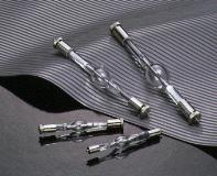
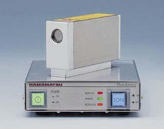
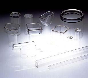
13 Electron Tube Photosensitive Electron Tubes, Light Sources & Image devices PMT(photomultiplier tubes): 90% share of the world market. PMT Flat Panel PMT Metal Package PMT Near Infrared PMT UV power meter Lamp Sources UV Spot Light Source MCP Photoionizer Glass Products Electron Multipliers HPD Image Intensifiers Scintillators EB-CCD 11
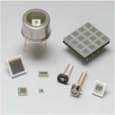
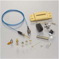
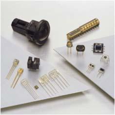
14 Opto-semiconductor Solid State Division Si Photodiodes APD MPPC Photo IC Image Sensors PSD Infrared Detectors Visible sensor Color sensors LED Optical Communication devices X-ray Flat Panel Sensors Mini-spectroscope Opt Semi-con. modules Automotive Devices LCOS-SLM 12


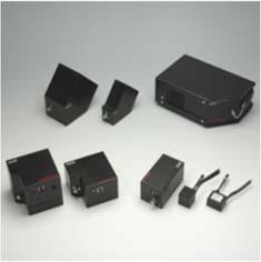
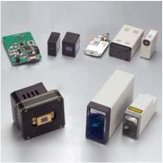
15 Imaging & Measurement s Systems Division Digital Camera Device High resolution sensitivity digital camera System for Life Science NanoZoomer, digital scanner Drug Screening System Semiconductor Failure Analysis 13
16 Experiments for High-Energy Physics Using Photomultiplier Tubes(PMT) Name of Experiment Purpose of Experiment Place of Exp. start year of production (plan) Number of Detectors Underground Hyper Neutrino, Proton Decay Japan ,000 -Kamiokande 14,000 LZ-7/DUSEL Dark Matter USA /180 JUNO (Daya Bay Ⅱ) Neutrino China ,000 Deep-sea Ice experiment Ground-surface KM3NeT Neutrino Europe ,000 Baikal-GVD Neutrino Russia ,000 IceCube/PINGU Neutrino Antarctic 2018 IceCube/HEX Neutrino Antarctic 2019 CTA Gamma-Ray Space Telescope Southern and Northern Hemisphere 60,000 ~ 78, ,000 ~ 300, ,000 Space Accelerator K-EUSO RICH/LHC-B/CERN Extreme energy cosmic ray particle Collision experiments(higgs) ISS ,000 Europe ,550 experiment RICH/CBM/GSI Fixed target experiment Europe ,100 14

17 Solid State Division (Opto-semiconductor Segment) New building at Shingai Factory Operations are scheduled to begin in May 2017 Buildng : Steel construction, 4 th floor(25m), Building area : 2,659m 2,, Floor area : 9,342m 2 Operation : Dicing, Assembly, Inspection Product : Chip-on-board, X-ray nondestructive, MPPC for medical, Automotive etc Capacity : In Shingai from 4 million / month to 10 million / month 15

18 Asia HAMAMATSU PHOTONICS K.K. Headquarters HAMAMATSU PHOTONICS (CHINA)Co., Ltd. Head Office / Shanghai Branch BEIJING HAMAMATSU PHOTON TECHNIQUES INC. Head Office / Langfang Factory HAMAMATSU PHOTONICS TAIWAN Co., Ltd. Hsinchu Office / Kaohsiung Office America HAMAMATSU CORPORATION Main Office / California Office / Chicago Office / Boston Office PHOTONICS MANAGEMENT CORP. Europe HAMAMATSU PHOTONICS EUROPE GmbH HAMAMATSU PHOTONICS DEUTSCHLAND GmbH Main Office / Netherlands Office / Poland Office / Danish Office HAMAMATSU PHOTONICS FRANCE S.A.R.L. Main Office / Swiss Office / Belgian Office / Spanish Office HAMAMATSU PHOTONICS NORDEN AB Main Office / Russian Office HAMAMATSU PHOTONICS ITALIA S.r.l. Main Office / Rome Office HAMAMATSU PHOTONICS UK Limited Main Office / South African Office
Hamamatsu Second Quarter Report (Summary) May 2018 Hamamatsu Photonics K.K. Tokyo Stock Exchange: 6965
 May 2018 Hamamatsu Photonics K.K. Tokyo Stock Exchange: 6965") Hamamatsu Second Quarter Report (Summary) Fiscal Year ending September 30, 2018 May 2018 Hamamatsu Photonics K.K. Tokyo Stock Exchange: 6965 www.hamamatsu.com Notes This material is not intended to be
Hamamatsu Second Quarter Report (Summary) Fiscal Year ending September 30, 2018 May 2018 Hamamatsu Photonics K.K. Tokyo Stock Exchange: 6965 www.hamamatsu.com Notes This material is not intended to be
Hamamatsu Third Quarter Databook. August 2018 Hamamatsu Photonics K.K.
 Hamamatsu Third Quarter Databook Fiscal ending September 30, 2018 August 2018 Hamamatsu Photonics K.K. Tokyo Stock Exchange: 6965 www.hamamatsu.com Notes This material is not intended to be a solicitation
David Castrillo Manager Spain-Portugal
 Digital Pathology Solutions by Hamamatsu Presentación para el Congreso Telepatología en Jerez. Noviembre 2014 David Castrillo +34 667 67 53 37 dcastrillo@hamamatsu.es Manager Spain-Portugal Who is Hamamatsu?
Photonic Devices for Vehicle Evolution
 Photonic Devices for Vehicle Evolution - The Latest in Optical MEMS and Solid State Photonics HAMAMATSU PHOTONICS UK Nov 2015 Jack Bennett Company Overview 4 Divisions Technology company, with focus on
Operating Results for the term ended Mar (the 73 rd term)
") The business performance briefing for the term ended Mar. 2011 (the 73 rd term) (Apr. 2010-Mar. 2011) EIKEN CHEMICAL CO., LTD. Apr. 28, 2011 EIKEN CHEMICAL CO., LTD. 1 Operating Results for the term ended
The business performance briefing for the term ended Mar. 2011 (the 73 rd term) (Apr. 2010-Mar. 2011) EIKEN CHEMICAL CO., LTD. Apr. 28, 2011 EIKEN CHEMICAL CO., LTD. 1 Operating Results for the term ended
Effective photosensitive area. Photosensitive area size
 High performance, high reliability Si PIN photodiodes The is a high-speed Si PIN photodiode having high sensitivity over a wide spectral range from visible to near infrared light. The provides high performance
Photosensitive area size (mm) Reverse voltage VR max (V) R to +60
 Reverse voltage VR max (V) R to +60") ,, 6 to 37 mm resistance length PSD for precision distance measurement Hamamatsu provides various types of one-dimensional PSD (position sensitive detector) designed for precision distance measurement
,, 6 to 37 mm resistance length PSD for precision distance measurement Hamamatsu provides various types of one-dimensional PSD (position sensitive detector) designed for precision distance measurement
Parameter Symbol Specification Unit Photosensitive area - ɸ0.8 mm Package mm
 Surface mount type, high-speed Si photodiode The is a Si PIN photodiode with sensitivities in the visible to near infrared range and is compatible with lead-free solder reflow. It features high-speed response
Short wavelength type APD. Effective photosensitive area (mm) Effective photosensitive area size* 2
 Effective photosensitive area size* 2") Short wavelength type APD Features High sensitivity at visible range Low noise High gain Low capacitance Applications Low-light-level measurement Analytical instrument Structure / Absolute maximum ratings
Short wavelength type APD Features High sensitivity at visible range Low noise High gain Low capacitance Applications Low-light-level measurement Analytical instrument Structure / Absolute maximum ratings
All-in-one solutions For applications with imaging challenges, we offer a wide range of TDI solutions.
 Speed Sensitivity Resolution All-in-one solutions For applications with imaging challenges, we offer a wide range of solutions. high-throughput Imaging in Low Light Applications New Generation of Solves
Reverse voltage VR max. Electrical and optical characteristics (Typ. Ta=25 C, unless otherwise noted) Short. Temp. S coefficient (A/W) of
 Short. Temp. S coefficient (A/W) of") Ceramic package photodiodes with low dark current The are ceramic package photodiodes that offer low dark current. Ceramic package used is light-impervious, so no stray light can reach the photosensitive
Ceramic package photodiodes with low dark current The are ceramic package photodiodes that offer low dark current. Ceramic package used is light-impervious, so no stray light can reach the photosensitive
Applications. Photosensitive area size. Storage temperature Tstg (mm) (mm 2 ) (V) ( C) ( C) S
 (mm 2 ) (V) ( C) ( C) S") , etc. Photodiodes molded into clear plastic packages These are Si photodiodes molded into clear plastic packages. Two types are available with sensitivity in the visible range and in the visible to near
, etc. Photodiodes molded into clear plastic packages These are Si photodiodes molded into clear plastic packages. Two types are available with sensitivity in the visible range and in the visible to near
Si PIN photodiodes. High-speed detectors with plastic package. Structure. Absolute maximum ratings
 High-speed detectors with plastic package The and are high-speed APC (auto power control) detectors developed for monitoring laser diodes with a peak wavelength of 66 nm or 78 nm. The is designed for surface
Non-discrete position sensors utilizing photodiode surface resistance
 Twodimensional PSD Nondiscrete position sensors utilizing photodiode surface resistance PSD (position sensitive detector) is an optoelectronic position sensor utilizing photodiode surface resistance. Unlike
1-D PSD with small plastic package
 1D PSD with small plastic package Hamamatsu offers a variety of 1D PSDs (position sensitive detectors) molded into plastic packages. These PSDs feature excellent position detection resolution, high resistance
16-element Si photodiode arrays
 Back-illuminated photodiode arrays for X-ray nondestructive inspection (element pitch: mm) The is a back-illuminated type 16-element photodiode array specifically designed for non-destructive X- ray inspection.
Effective photosensitive* 2 area size. Storage temperature Tstg (mm) ( C) ( C) S φ0.2 φ0.5 S φ to to +100 S9075
 ( C) ( C) S φ0.2 φ0.5 S φ to to +100 S9075") /-05/-10, S5344, S5345 Short wavelength type APD, for 600 nm band These are short wavelength APDs with improved sensitivity in the UV to visible range. They offer high gain, high sensitivity, and low noise
/-05/-10, S5344, S5345 Short wavelength type APD, for 600 nm band These are short wavelength APDs with improved sensitivity in the UV to visible range. They offer high gain, high sensitivity, and low noise
These Si photodiodes have sensitivity in the UV to near IR range. They are suitable for low-light-level detection in analysis and the like.
 UV to near IR for precision photometry These Si photodiodes have sensitivity in the UV to near IR range. They are suitable for low-light-level detection in analysis and the like. Features High sensitivity
16-element Si photodiode arrays
 Back-illuminated photodiode arrays for X-ray nondestructive inspection (element pitch: mm) The is a back-illuminated type 16-element photodiode array specifically designed for non-destructive X-ray inspection.
Low bias operation, for 800 nm band
 Low bias operation, for 800 nm band These are 800 nm band near-infrared Si APDs that can operate at low voltages, 200 V or less. They are suitable for applications such as FSO (free space optics) and optical
Effective photosensitive area (mm) Photosensitive area size
 Photosensitive area size") High UV resistance, photodiodes for UV monitor The are Si photodiodes that have achieved high reliability for monitoring ultraviolet light by employing a structure that does not use resin. They exhibit
High UV resistance, photodiodes for UV monitor The are Si photodiodes that have achieved high reliability for monitoring ultraviolet light by employing a structure that does not use resin. They exhibit
Suppressed IR sensitivity
 For UV to visible, precision photometry; suppressed IR sensitivity These Si photodiodes have suppressed IR sensitivity. They are suitable for low-light-level detection in analysis and the like. Features
JVC Reports Business Results for Fiscal 2006 (April 1, 2005 March 31, 2006)
") For Immediate Release: April 27, 2006 JVC Reports Business Results for Fiscal 2006 Victor Company of Japan, Ltd. (JVC) announced today its financial results for fiscal 2006. Consolidated total sales decreased
For Immediate Release: April 27, 2006 JVC Reports Business Results for Fiscal 2006 Victor Company of Japan, Ltd. (JVC) announced today its financial results for fiscal 2006. Consolidated total sales decreased
RGB color sensor. Effective photosensitive area. Green, Red: 2.25 Blue : 4.5
 Si photodiodes S6428-01 S6429-01 S6430-01 RGB color sensor The S6428-01, S6429-01 and S6430-01 are color sensors designed to respectively detect monochromatic colors of blue (λp=460 nm), green (λp=540
Effective photosensitive area (mm)
") Chip carrier package for mount The, S5107, and S7510 are Si PIN photodiodes sealed in chip carrier packages suitable for mount using automated solder reflow techniques. These photodiodes have large photosensitive
Chip carrier package for mount The, S5107, and S7510 are Si PIN photodiodes sealed in chip carrier packages suitable for mount using automated solder reflow techniques. These photodiodes have large photosensitive
Parameter Specification Unit Photosensitive area mm Package Glass epoxy - Seal material Silicone resin -
 COB type, applicable to lead-free solder reflow The is a for visible to near infrared range and is compatible with lead-free solder reflow processes. The small and thin leadless package allows reducing
MPPC modules. MPPC array modules for very-low-level light detection, 16 ch analog output. C13368/C13369 series (Analog output type)
") MPPC modules C13368/C13369 series (Analog output type) MPPC array modules for very-low-level light detection, 16 ch analog output The C13368/C13369 series (analog output type) is an optical measurement
MPPC modules C13368/C13369 series (Analog output type) MPPC array modules for very-low-level light detection, 16 ch analog output The C13368/C13369 series (analog output type) is an optical measurement
16-element Si photodiode arrays
 S11299-321 S11299-421 S11299-21 S11299-121 Back-illuminated photodiode arrays for X-ray non-destructive inspection, slender board type The is a back-illuminated type 16-element photodiode array specifically
UV-LED MODULE. UV Irradiation Intensity Distribution Graphs
 UV-LED MODULE UV Irradiation Intensity Distribution Graphs Product Lineup Lens Lineup Product Lineup LED DRIVER C1559-1 LED HEAD UNIT L1561/L196 SERIES standard type standard type high power type high
High-speed photodiodes (S5973 series: 1 GHz)
") S5973 series High-speed photodiodes (S5973 series: 1 GHz), and S5973 series are high-speed Si PIN photodiodes designed for visible to near infrared light detection. These photodiodes provide wideband characteristics
S5973 series High-speed photodiodes (S5973 series: 1 GHz), and S5973 series are high-speed Si PIN photodiodes designed for visible to near infrared light detection. These photodiodes provide wideband characteristics
MPPC (Multi-Pixel Photon Counter)
") S13362-35DG Significantly reduced crosstalk, low afterpulses The can reduce dark count by cooling in addition to low afterpulses and low crosstalk of the S1336 series. The integrates the S1336 series with
S13362-35DG Significantly reduced crosstalk, low afterpulses The can reduce dark count by cooling in addition to low afterpulses and low crosstalk of the S1336 series. The integrates the S1336 series with
InAsSb photovoltaic detectors
 High-speed response and high sensitivity in the spectral band up to 11 μm Infrared detectors The are photovoltaic type infrared detectors that have achieved high sensitivity in the spectral band up to
Si PIN photodiodes. High-speed detectors with plastic package. Structure. Absolute maximum ratings
 High-speed detectors with plastic package The and are high-speed APC (auto power control) detectors developed for monitoring laser diodes with a peak wavelength of 66 nm or 78 nm. The is designed for surface
InAsSb photovoltaic detector
 InAsSb photovoltaic detector P12691-21 High-speed response and high sensitivity in the 8 μm spectral band Thermoelectrically cooled infrared detector with no liquid nitrogen required The P12691-21 is an
Parameter Specification Unit Photosensitive area mm Package Glass epoxy - Seal material Epoxy resin -
 COB type, applicable to lead-free solder reflow The is a Si PIN photodiode for visible to near infrared range and is compatible with lead-free solder reflow processes. The small and thin leadless package
*Amounts less than 100 million yen shown in this presentation material have been rounded down. Copyright 2011 SHARP CORPORATION, All Rights Reserved.
 Business Strategy for FY211 Ⅰ.. Forecast for FY211 Financial Results Ⅱ.. LCD Business Restructuring SHARP CORPORATION Mikio Katayama, President June 3, 211 1 Forward-Looking Statements This presentation
NMOS linear image sensor
 Image sensor highly sensitive to X-rays from 0 k to 00 kev s are self-scanning photodiode arrays designed specifically as detectors for multichannel spectroscopy. The scanning circuit is made up of N-channel
Review of High Quantum Efficiency Large Area Photomultiplier Tubes
 Jinping Solar Neutrino Workshop, LBNL, June 2014 Review of High Quantum Efficiency Large Area Photomultiplier Tubes Jianglai Liu Shanghai Jiao Tong University 2014/6/10 Disclaimer: I am not personally
Photosensitive area (mm) 4 4. Peak sensitivity wavelength (nm) Supply voltage Dark state. Max. Vcc max. Tstg Min. Max. (ma) (V)
 4 4. Peak sensitivity wavelength (nm) Supply voltage Dark state. Max. Vcc max. Tstg Min. Max. (ma) (V)") Integrates a PSD for precision photometry or a 4-segment Si photodiode with low-noise amp in a compact case PSD modules contain a high-precision two-dimensional PSD (position sensitive detector) or a 4-segment
Integrates a PSD for precision photometry or a 4-segment Si photodiode with low-noise amp in a compact case PSD modules contain a high-precision two-dimensional PSD (position sensitive detector) or a 4-segment
MCT photoconductive detectors
 Non-cooled type and suitable for long, continuous operation Features Choice of spectral response (up to 12 μm) The band gap can be adjusted by controlling the composition ratio of HgTe and CdTe. Utilizing
Peak sensitivity wavelength λp (nm) Photosensitive area (mm)
 Photosensitive area (mm)") Integrates a -PSD for precision photometry or a 4-segment Si photodiode with low-noise amp in a compact case PSD modules contain a high-precision two-dimensional PSD (position sensitive detector) or a
Integrates a -PSD for precision photometry or a 4-segment Si photodiode with low-noise amp in a compact case PSD modules contain a high-precision two-dimensional PSD (position sensitive detector) or a
MCT photoconductive detectors
 MCT photoconductive detectors P3257 series P4249-08 0 μm band infrared detector with high sensitivity and high-speed response Features High-speed response, high sensitivity in the 0 μm band detection Photoconductive
SOLID STATE DIVISION. Selection Guide Feb LED. Wide variations of Light Emitting Diodes to match various applications
 SOLID STATE DIVISION Selection Guide Feb. 2 LED Wide variations of Light Emitting Diodes to match various applications LED LIGHT EMITTING DIODES HAMAMATSU offers a broad lineup of light emitters such as
InGaAs PIN photodiode arrays
 16/32/46 element InGaAs array for near IR detection The is one-dimensional InGaAs PIN photodiode array in a ceramic DIP (dual inline package). It can be used to perform simple spectroscopic analysis. Features
JVC Reports Business Results for the First Half of Fiscal 2006
 For Immediate Release: October 27, 2005 JVC Reports Business Results for the First Half of Fiscal 2006 (April 1, 2005- September 30, 2005) Victor Company of Japan, Ltd. (JVC) announced today it registered
Photon counting module
 Photon counting module Fiber coupling type, low-light-level detection The is a photon counting module that can detect low-level light. It consists of a TE-cooled single pixel photon counter (SPPC), signal
Application OCT. Dimensions (mm) Weight (g) Operating temperature* 1 Storage temperature* 1 λ=1.55 μm (V) (mw)
 Weight (g) Operating temperature* 1 Storage temperature* 1 λ=1.55 μm (V) (mw)") Balanced detectors with reduced multiple reflections These are differential amplification type photoelectric conversion modules containing two Hamamatsu photodiodes with balanced characteristics. The photodiodes
Balanced detectors with reduced multiple reflections These are differential amplification type photoelectric conversion modules containing two Hamamatsu photodiodes with balanced characteristics. The photodiodes
16-element Si photodiode arrays
 S11212-421 S11212-321 S11212-021 S11212-121 Back-illuminated photodiode arrays for non-destructive inspection The is a back-illuminated type 16-element photodiode array specifically designed for non-destructive
APD modules. APD module integrated with peripheral circuits. C12703 series. Selection guide. Block diagram
 APD module integrated with peripheral circuits Features Uses a high sensitivity APD Two types of APDs with different photosensitive areas (φ1.5 mm, φ3. mm) are provided. On-board high sensitivity circuit
Accessories for infrared detector
 Temperature controllers Heatsinks for TE-cooled detector Chopper, etc. Wide lineups of accessories for infrared detector HAMAMATSU provides temperature controllers, heatsinks for TE-cooled detector, chopper
InAsSb photovoltaic detector
 InAsSb photovoltaic detector P2-2 High-speed response and high sensitivity in the 5 μm spectral band Thermoelectrically cooled infrared detector with no liquid nitrogen required The P2-2 is an infrared
MPPC (multi-pixel photon counter)
") MPPC (multi-pixel photon counter) Low afterpulses, wide dynamic range, for high-speed measurement Photosensitive area: 1 1 mm These MPPCs utilize very small pixels arrayed at high densities to achieve
MPPC (multi-pixel photon counter) Low afterpulses, wide dynamic range, for high-speed measurement Photosensitive area: 1 1 mm These MPPCs utilize very small pixels arrayed at high densities to achieve
YXLON Cougar EVO PLUS
 YXLON Cougar EVO PLUS The best small footprint X-ray inspection system for LABORATORY applications Technology with Passion Choose a custom-built EVO solution for premium inspection Why compromise? As technology
PbSe photoconductive detectors
 PbSe photoconductive detectors P9696 series P327-8 Infrared detectors with fast response and high sensitivity in 5 μm wavelength band Compared to other detectors used in the same wavelength regions, PbSe
InGaAs multichannel detector head
 Near infrared line camera (Line rate: 31.25 khz) The is a multichannel detector head suitable for applications where high-speed response is required, such as SD- OCT (spectral domain-optical coherence
Photoemission microscope HAMAMTSU PHEMOS-1000 ONPY-PEM
 Photoemission microscope HAMAMTSU PHEMOS-1000 ONPY-PEM Extended resources for Failure Analysis (FA) in ONPY Subject: Benefits for ONPY from participating on 5th European Workshop on Photonics Failure Analysis
Production and Development status of MPPC
 Production and Development status of MPPC Kazuhisa Yamamura 1 Solid State Division, Hamamatsu Photonics K.K. Hamamatsu-City, 435-8558 Japan iliation E-mail: yamamura@ssd.hpk.co.jp Kenichi Sato, Shogo Kamakura
Si photodiode. Applicable to lead-free solder reflow and wide temperature range. S9674. Absolute maximum ratings
 Applicable to lead-free solder reflow and wide temperature range The is a photodiode that is applicable to lead-free solder reflow and has an extremely wide operating and storage temperature range (-40
Photo IC diode. Wide operating temperature: -40 to +105 C. S MT. Absolute maximum ratings (Ta=25 C)
") Wide operating temperature: -40 to +05 C The photo IC has a spectral response close to human eye sensitivity. Two active areas are made on a single chip. Almost only the visible range can be measured by
Wide operating temperature: -40 to +05 C The photo IC has a spectral response close to human eye sensitivity. Two active areas are made on a single chip. Almost only the visible range can be measured by
Photo IC diode. Plastic package shaped the same as metal package. S SB. Features. Applications
 Plastic package shaped the same as metal package The photo IC has spectral response close to human eye sensitivity. Two photosensitive areas are made on a single chip. Almost only the visible range can
APD modules. Operates an APD with single 5 V supply (standard type, short-wavelength type) C12702 series.
 C12702 series.") Operates an APD with single 5 V supply (standard type, short-wavelength type) Features Includes a high-sensitivity APD Uses a Hamamatsu high-sensitivity Si APD. Four types are available with different
Operates an APD with single 5 V supply (standard type, short-wavelength type) Features Includes a high-sensitivity APD Uses a Hamamatsu high-sensitivity Si APD. Four types are available with different
VTA0832H Series Linear Photodiode Array (PDA) for X-ray Scanning
 for X-ray Scanning") DATASHEET Photon Detection VTA0832H Series VTA0832H-L-NC-00-0 The VTA0832H series is a 32-channel High Resolution Photodiode Array (PDA). There are 16 dual-element photodiodes mounted directly on an FR-4
DATASHEET Photon Detection VTA0832H Series VTA0832H-L-NC-00-0 The VTA0832H series is a 32-channel High Resolution Photodiode Array (PDA). There are 16 dual-element photodiodes mounted directly on an FR-4
Infrared detector modules with preamp
 Easy-to-use detector modules with built-in preamps Infrared detector modules operate just by connecting to DC power supplies. The detector element is selectable from among InGaAs, InAs, InSb, and InAsSb
Signal processing circuit for 2-D PSD
 Signal processing circuit for 2-D PSD Circuit board for easier 2-D PSD operation The is a DC signal processing circuit for two-dimensional PSD. It is suitable for displacement measurements using DC light.
Optics modules. Absorbance measurement module with built-in photodiode array, optical elements, current-tovoltage. C13398 series.
 Absorbance measurement module with built-in photodiode array, optical elements, current-tovoltage converter, etc. The is an optics module for absorbance measurement featuring high blocking performance
VTA1216H Series Linear Photodiode Array (PDA) for X-ray Scanning
 for X-ray Scanning") DATASHEET Photon Detection VTA1216H Series VTA1216H-L-SC-08-1 The VTA1216H series is a 16-channel High Resolution Photodiode Array (PDA). There are 8 dual-element photodiodes mounted directly on an FR-4
DATASHEET Photon Detection VTA1216H Series VTA1216H-L-SC-08-1 The VTA1216H series is a 16-channel High Resolution Photodiode Array (PDA). There are 8 dual-element photodiodes mounted directly on an FR-4
Peak emission wavelength: 3.9 μm
 Peak emission wavelength: 3.9 μm The is a high-output mid-infrared LED with a 3.9 µm peak emission wavelength. It is a product that has been achieved using Hamamatsu unique crystal growth technology and
Between elements measure. Photosensitive area (per 1 element)
") 16, 35, 46 element Si photodiode array for UV to NIR The are Si photodiode linear array mounted in ceramic DIPs (Dual Inline Packages). These photodiode arrays are primarily developed for low-light-level
16, 35, 46 element Si photodiode array for UV to NIR The are Si photodiode linear array mounted in ceramic DIPs (Dual Inline Packages). These photodiode arrays are primarily developed for low-light-level
Photo IC diode. Plastic package shaped the same as metal package. S SB. Absolute maximum ratings (Ta=25 C)
") Plastic package shaped the same as metal package The photo IC has spectral response close to human eye sensitivity. Two photosensitive areas are made on a single chip. Almost only the visible range can
Plastic package shaped the same as metal package The photo IC has spectral response close to human eye sensitivity. Two photosensitive areas are made on a single chip. Almost only the visible range can
Signal processing circuit for 2-D PSD
 Signal processing circuit for 2-D PSD Circuit board for easier 2-D PSD operation The is a DC signal processing circuit for two-dimensional PSD. It is suitable for displacement measurements using DC light.
InAsSb photovoltaic detectors
 High-speed response and high sensitivity in the spectral band up to 5 μm Infrared detectors The are photovoltaic type infrared detectors that have achieved high sensitivity in the spectral band up to 5
u EVS FABRIQ VISION The fabric quality assurance system Technical Data
 u EVS FABRIQ VISION Technical Data October 2018 USTER EVS FABRIQ VISION ensures this is achieved, by using automated control during intermediate and final inspection. The system s ability to capture any
Peak emission wavelength: 4.3 μm
 Peak emission wavelength: 4.3 μm The is a mid infrared LED with a 4.3 μm peak emission wavelength. It is a product that has been achieved using Hamamatsu unique crystal growth technology and process technology.
M=100, RL=50 Ω λ=800 nm, -3 db
 Low bias operation, for 800 nm band, small package Features Miniature and thin package:.8 3..0 t mm Stable operation at low bias High-speed response High sensitivity Low noise Applications Optical rangefinder
Maximum reliability for the most aggressive environments. Encoder and motor feedback systems for wind power systems
 Industry Guide Maximum reliability for the most aggressive environments Encoder and motor feedback systems for wind power systems SICK STEGMANN a successful SICK Group company With customer-focused products,
Large photocathode 20-inch PMT testing methods for the JUNO experiment
 Large photocathode 20-inch PMT testing methods for the JUNO experiment N. Anfimov a on behalf of the JUNO collaboration. a Joint Institute for Nuclear Research, 141980, 6 Joliot-Curie, Dubna, Russian Federation
Explore the Art of Detection
 Y.Cougar Microfocus and nanofocus X-ray inspection systems for the electronics industries Explore the Art of Detection Technology with Passion Our specialty: The Art of Detection. Developing outstanding
Variable gain and stable detection even at high gains
 MODULE APD module C5 Variable gain and stable detection even at high gains Along with an APD, current-to-voltage conversion circuit, and high-voltage power supply circuit, the C5 contains a microcontroller
APD module. Variable gain, stable detection even at high gain. C Applications. Features. Sensitivity vs.
 APD module C158-1 Variable gain, stable detection even at high gain The C158-1 consists of an APD, current-to-voltage converter, high-voltage power supply circuit as well as a microcontroller for compensating
Photosensor with front-end IC
 Compact APD suitable for various light level detection The is a compact optical device that integrates a Si APD and preamp. It has a built-in DC feedback circuit for reducing the effects of background
Signal processing circuit for 1-D PSD
 Signal processing circuit for 1-D PSD Circuit board for easier 1-D PSD operation The is a DC signal processing circuit for one-dimensional PSD. It is suitable for displacement measurements using DC light.
LCOS-SLM (Liquid Crystal on Silicon - Spatial Light Modulator)
") POWER LCOS-SLM CONTROLLER RESET POWER OUTPUT ERROR LCOS-SLM (Liquid Crystal on Silicon - Spatial Light Modulator) Control your light! Shape your beam! Improve your image! The devices are a reflective type
POWER LCOS-SLM CONTROLLER RESET POWER OUTPUT ERROR LCOS-SLM (Liquid Crystal on Silicon - Spatial Light Modulator) Control your light! Shape your beam! Improve your image! The devices are a reflective type
Signal processing circuit for 1-D PSD
 Signal processing circuit for 1-D PSD Circuit board for easier 1-D PSD operation The is a DC signal processing circuit for one-dimensional PSD. It is suitable for displacement measurements using DC light.
MPPC modules. Photon counting module with built-in MPPC. C series C10751 series. Selection guide
 C10507-11 series C10751 series Photon counting module with built-in MPPC The MPPC (multi-pixel photon counter) module is a photon counting module capable of low-light-level detection. This module consists
MPPC (Multi-Pixel Photon Counter)
") MPPC (Multi-Pixel Photon Counter) MPPCs in a chip size package miniaturized through the adoption of TSV structure The are MPPCs for precision measurement miniaturized by the use of TSV (through-silicon
MPPC (Multi-Pixel Photon Counter) MPPCs in a chip size package miniaturized through the adoption of TSV structure The are MPPCs for precision measurement miniaturized by the use of TSV (through-silicon
Artisan Technology Group is your source for quality new and certified-used/pre-owned equipment
 Artisan Technology Group is your source for quality new and certified-used/pre-owned equipment FAST SHIPPING AND DELIVERY TENS OF THOUSANDS OF IN-STOCK ITEMS EQUIPMENT DEMOS HUNDREDS OF MANUFACTURERS SUPPORTED
S P. Ultra-miniature, high performance Electromagnetically driven laser scanning MEMS mirror. Features.
 Si MEMS photodiode mirror Ultra-miniature, high performance Electromagnetically driven laser scanning MEMS mirror The is an electromagnetically driven mirror that incorporates our unique MEMS (micro-electro-mechanical
Bio-Rad Imaging Systems Family
 www.bio-rad.com/imagingsystems Imaging Bio-Rad Imaging Systems Family Unlike other imagers, Bio-Rad imaging systems were developed by scientists for scientists. Bio-Rad understands your challenges and
Driver circuits for CCD image sensor
 Driver circuit for CCD image sensor (S10420/S11071/S11510 series) The and are driver circuits designed for HAMAMATSU CCD image sensor S10420/S11071/S11510 series. The and can be used in spectrometer when
New Medical Light Source using NTT s Communication Laser Technology
 (Press release document) January 31, 2013 NTT Advanced Technology Corporation Hamamatsu Photonics K.K. New Medical Light Source using NTT s Communication Laser Technology - NTT-AT and Hamamatsu Photonics
STMicroelectronics Proximity Sensor & Flood Illuminator Time of Flight & Illumination device from Apple iphone X
 STMicroelectronics Proximity Sensor & Flood Illuminator Time of Flight & Illumination device from Apple iphone X IMAGING report by Stéphane ELISABETH January 2018 version 1 21 rue la Noue Bras de Fer 44200
Driver circuit for MPPC
 Simple evaluation starter kit for non-cooled s The is a starter kit designed for simple non-cooled evaluations. It consists of a sensor board and a power supply board. The sensor board includes an socket
Near infrared image sensor (0.9 to 1.7 µm) with high-speed data rate
 with high-speed data rate") IMAGE SENSOR InGaAs linear image sensor G99-56D/-5D Near infrared image sensor (.9 to.7 µm) with high-speed data rate HAMAMATSU provides high-speed, near infrared image sensors designed for detectors used
IMAGE SENSOR InGaAs linear image sensor G99-56D/-5D Near infrared image sensor (.9 to.7 µm) with high-speed data rate HAMAMATSU provides high-speed, near infrared image sensors designed for detectors used
Global Invacom Group Limited. FY2014 Results Presentation 26 February 2015
 Global Invacom Group Limited FY2014 Results Presentation 26 February 2015 Presentation Outline 1 Global Invacom Overview 2 Recent Corporate Developments 3 FY2014 Financial Highlights 4 Strategy, Outlook
YEEBO Group. Date August 2010
 YEEBO Group Date August 2010 Profile Name YEEBO LCD LTD Start 1988 年 Capaital US$51.5 Million or HKD 402 Million Turnover US$83.3 Million or HKD 650 Million (2007~2008) Employees 2,500 Headquarter 7/F.,
Selection Criteria for X-ray Inspection Systems for BGA and CSP Solder Joint Analysis
 Presented at Nepcon Shanghai 2003 Abstract Selection Criteria for X-ray Inspection Systems for BGA and CSP Solder Joint Analysis Dr. David Bernard, Dage Precision Industries, 158-29 Hua Shan Road, Feng
Create an Industrial 3D Machine Vision System using DLP Technology
 Create an Industrial 3D Machine Vision System using DLP Technology -AM572x Processor based DLP Structured Light Terry Yuan Business Development Manager 1 1987 TI DLP Products: A History of Innovation Dr.
Photo IC diode. COB (chip on board) type, small package. S CT. Absolute maximum ratings
 type, small package. S CT. Absolute maximum ratings") COB (chip on board) type, small package mm The photo IC has spectral response close to human eye sensitivity. Two photosensitive areas are made on a single chip. Almost only the visible range can be measured
COB (chip on board) type, small package mm The photo IC has spectral response close to human eye sensitivity. Two photosensitive areas are made on a single chip. Almost only the visible range can be measured
WAFER PROBER MODEL. IR-OBIRCH analysis system Infra Red - Optical Beam Induced Resistance CHange AMOS -200
 WAFER PROBER MODEL IR-OBIRCH analysis system Infra Red - Optical Beam Induced Resistance CHange AMOS -200 IR-OBIRCH Analysis System The μamos is a semiconductor failure analysis system which uses IR-OBIRCH
Photo IC for optical switch
 Photo IC with optical switch functions The S6841 and S8119 are specifically designed for optical switches. A transmission mode or reflection mode optical switch can be easily configured when used in combination