|
|
|
- Bernadette Pitts
- 5 years ago
- Views:
Transcription
1 Synchronizers for Asynchronous Signals Asynchronous signals causes the big issue with clock domains, namely metastability. This is a situation where the clock domain trying to capture the asynchronous event goes into a metastable state. Is the asychronous signal a logic 1 or a logic 0 state? Metastability cannot be prevented but it can be reduce. High-speed digital circuits rely on synchronizers to create a time buffer for recovering from a metastable event, thereby reducing the possibility that metastability will cause a circuit to malfunction. EDA companies such as Synopsys, Cadence and Mentor Graphics, create software to automatically read verilog code and detect synchronization problems. There are two basic types of synchronizers: 1) Asynchronous signal wider than the clock period of the synchronizer clock domain and 2) Asynchronous signal smaller than the clock period of the synchronizer clock domain. Asynchronous signal > Synchronizer clock period If designed into an ASIC (Application Specific Integrated Circuit), this synchronizer is typically put into a special library cell to keep the two back to back D flip-flop close to each other functionally and to minimize any clock skew in the ASIC. In addition, as a rule of thumb, this synchronizer usually has a special cell name like sync_ss, meaning synchronize slow input signal. 1
2 Asynchronous signal < Synchronizer clock period Similar to the circuit above, this synchronizer is typically put into a special library cell to keep the D flip-flops and special logic close to each other for functionality purposes and to minimize any clock skew in the ASIC. In addition, as a rule of thumb, this synchronizer usually has a special cell name like sync_fs, meaning synchronize fast input signal. 2
3 AS DIGITAL DESIGN BECOMES INCREASINGLY SOPHISTICATED, CIRCUITS WITH MULTIPLE CLOCKS MUST RELIABLY COMMUNICATE WITH EACH OTHER When signals travel from one clock domain to another, the signal appears to be asynchronous in the new clock domain. The circuit that receives this signal needs to synchronize it. Synchronization prevents the metastable state of the first storage element (flip-flop) in the new clock domain from propagating through the circuit. Metastability is the inability of a flip-flop to arrive at a known state in a specific amount of time. When a flip-flop enters a metastable state, you can predict neither the element s output voltage level nor when the output will settle to a correct voltage level. During this settling time, the flip-flop s output is at some intermediate voltage level or may oscillate and can cascade the invalid output level to flip-flops farther down the signal path. The input must be stable during a small window of time around the active edge of the clock for any flip-flop. FPGA manufacturers and IC foundries qualify their flip-flops and determine their characteristics. MTBF (mean time between failures) describes the metastability characteristic of a flip-flop using statistics to determine the probability of a flip-flop s failure. Manufacturers base the MTBF in part on the length of the time window during which a change in the input signal causes the flip-flop to become unstable. In addition, MTBF calculation uses the frequency of the input signal and the frequency of the clock driving the flip-flop. 3
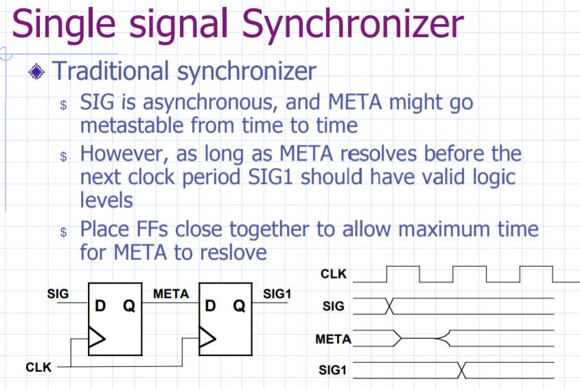
4 Each type of flip-flop in an ASIC or FPGA library has timing requirements to help you determine the window of vulnerability. Setup time describes the time an input signal to a flip-flop must be stable before the clock edge. Hold time is the time the signal must remain stable after the clock edge. These specifications are usually conservative to account for all the possible variations in supply voltage, operating temperature, signal quality, and fabrication. If a design meets these timing requirements, the possibility is negligible that the flip-flop will fail. Synthesis programs in modern IC and FPGA designs ensure that digital circuits meet the setupand-hold requirements for each flip-flop in the design; however, asynchronous signals pose problems for the software. A signal crossing a clock domain appears to be asynchronous to the logic in the new clock domain. SIGNAL SYNCHRONIZATION The purpose of synchronizing signals is to protect downstream logic from the metastable state of the first flip-flop in a new clock domain. A simple synchronizer comprises two flip-flops in series without any combinational circuitry between them. This design ensures that the first flip-flop exits its metastable state and its output settles before the second flip-flop samples it. You also need to place the flip-flops close to each other to ensure the smallest possible clock skew between them. IC foundries help with signal synchronization by providing synchronizer cells. These cells usually comprise a flip-flop with a very high gain that uses more power and is larger than a standard flip-flop. Such a flip-flop has reduced setup-and hold-time requirements for the input signal and is resistant to oscillation when the input signal causes a metastable condition. 4

5 For synchronization to work properly, the signal crossing a clock domain should pass from flipflop in the original clock domain to the first flip-flop of the synchronizer without passing through any combinational logic between the two. This requirement is important because the first stage of a synchronizer is sensitive to glitches that combination logic produces. A synchronized signal is valid in the new clock domain after two clock edges. The signal delay is between one and two clock periods in the new clock domain. A rule of thumb is that a synchronizer circuit causes two clock cycles of delay in the new clock domain. 5

6 The edge-detecting synchronizer circuit adds a flip-flop to the output of the level synchronizer. This circuit detects the rising edge of the input to the synchronizer and generates a clockwide, active-high pulse. Switching the inverter on the AND gate inputs creates a synchronizer that detects the falling edge of the input signal. Changing the AND gate to a NAND gate results in a circuit that generates an active-low pulse. The edge-detecting synchronizer works well at synchronizing a pulse going to a faster clock domain. This circuit produces a pulse that indicates the rising or falling edge of the input signal. One restriction of this synchronizer is that the width of the input pulse must be greater than the period of the synchronizer clock plus the required hold time of the first synchronizer flipflop. The safest pulse width is twice the synchronizer clock period. This synchronizer does not work if the input is a single clock wide pulse entering a slower clock domain. 6

7 The input signal of a pulse synchronizer is a single clockwide pulse that triggers a toggle circuit in the originating clock. The output of the toggle circuit switches from high to low and vice versa each time it receives a pulse and passes through the level synchronizer to arrive at one input of the XOR gate, while a one-clock-cycle-delayed version goes to the other input of the XOR. For one clock cycle, each time the toggle circuit changes state, the output of this synchronizer generates a single clockwide pulse. The basic function of a pulse synchronizer is to take a single clockwide pulse from one clock domain and create a single clockwide pulse in the new domain. One restriction of a pulse synchronizer is that input pulses must have a minimum spacing between pulses equal to two synchronizer clock periods. If the input pulses are closer, the output pulses in the new clock domain are adjacent to each other, resulting in an output pulse that is wider than one clock cycle. This problem is more severe when the clock period of input pulse is greater than twice the synchronizer clock period. In this case, if the input pulses are too close, the synchronizer does not detect every one. 7
8 8
9 9
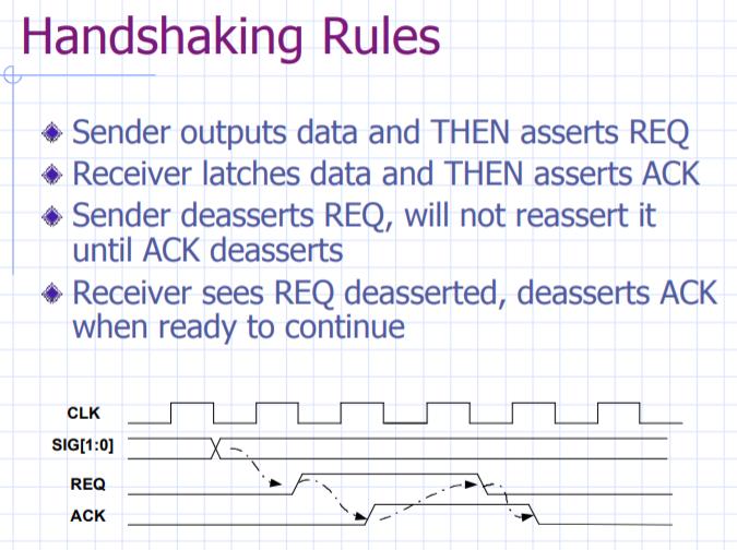
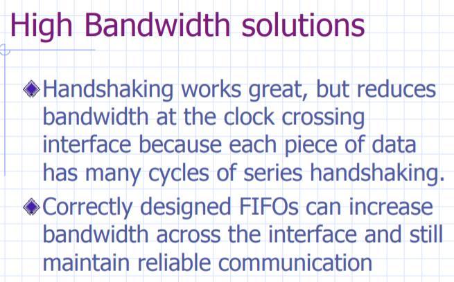
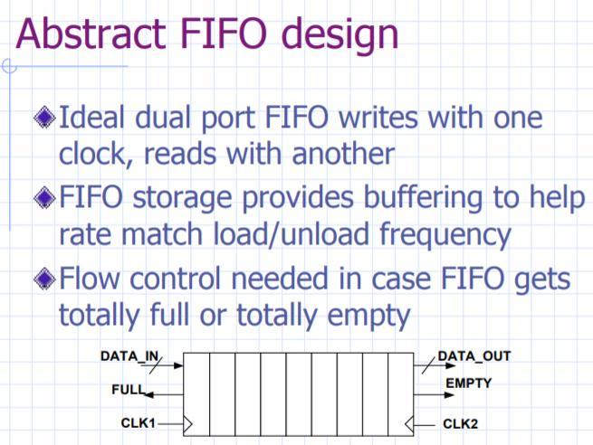
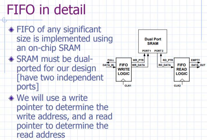
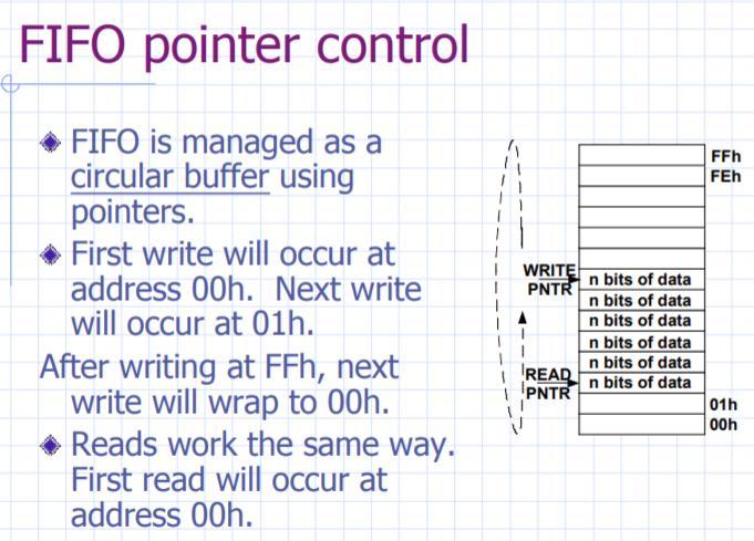
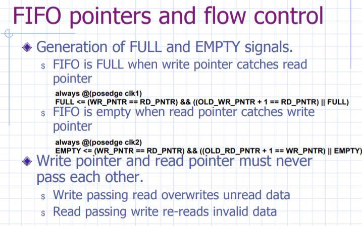
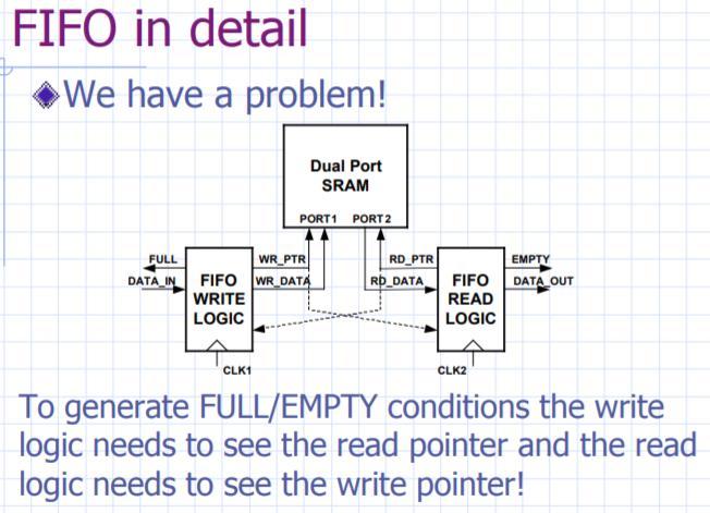
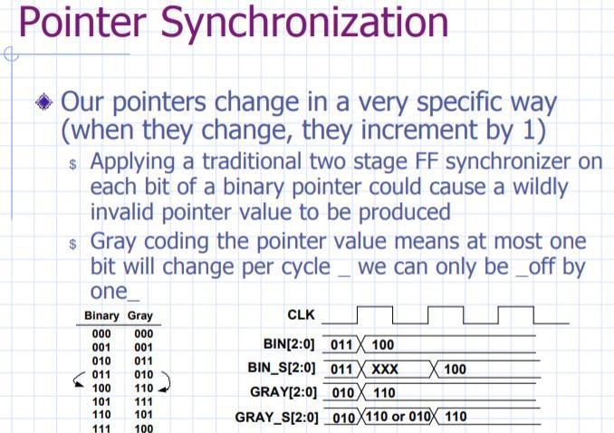
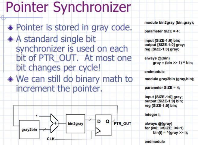
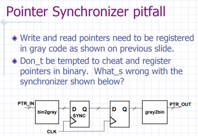
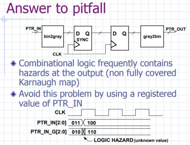
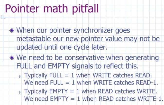
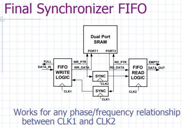
10 Bus Synchronization Obvious approach is to use single signal synchronizers on each bit : WRONG! Handshaking is the Answer 10
11 11
12 12
13 13
14 14
15 15
16 16
17 17
18 18
19 19
20 20
21 21
22 22
23 23
24 24
25 Some synchronization problems with logic in FPGA Problem to solve: If an external asynchronous signal is used inside a synchronous system it needs to be synchronized before use. Why? 1. Metastability problem 2. At the same clk sampling time (i.e. rising_edge(clk)), all the logic elements using this signal and clocking it, need to see it at the same logical level!! Metastability problem: To be correctly sampled by a FF (Flip-Flop or D-register) a signal (D) needs to respect 2 very important timings: tsu: Set up time: D valid before Clk thold: Hold time: D stay valid after Clk 25

26 If the rule is NOT respected: The output can be '0' or '1' good The output can be in an intermediate level for an undefined time metastable level DFF.. Sampling of input signals The level of the metastable signal is between the '0' and the '1'. The time the metastable signal stays is probabilistic and theoretically could be infinitive. Practically it disappears at the next signal sampling. Usually a DFF sampling a metastable level would not propagate it. As for this intermediate level, a decision is take for a '0' or a '1'. It could propagate to a next DFF if the level change just at the sampling point to the metastable threshold, the probability is very low but not 0! Thus depending on the hardness of the design to do, more DFF are needed. Manufacturer provides information about the parameters for metastability. 26


27 DFF.. Sampling of input signals View of the same value for all the sampling FF. If the rule is NOT respected: Very bad for 1 DFF worst if the same signal D is going to more than 1 DFF: each DFF could see a different input level Qa, Qb : 2 different DFF outputs 27
, all the logics using the signal and clocking it, need to see")
28 DFF.. Sampling of input signals At the same clk sampling time (i.e. rising_edge), all the logics using the signal and clocking it, need to see it at the same logic level!! A synchronizing system is necessary 28


29 DFF.. Sampling of input signals The first DFF can have a metastable signal as output Qm The second one will probably filter it For very high reliability system more DFF could be necessary, delay added!! DFF.. Sampling of input signals Async Input The Qsn signal can be used by all the logic that need it: the level will be the same for all the logic elements 29
30 DFF.. Sampling of input signals Clock distribution Inside the FPGA all the DFF using the same D signal need to use the same Clock. Special global lines are available inside a FPGA for that purpose. They are limited in number. If we expect to use a normal signal as a clock for a FF it's a very bad idea We need to use the Clock Enable feature of a DFF in a FPGA DFF.. Conclusion Asynchronous signals need to be synchronized before use in a FPGA A simple DFF can generate metastable output At least a second DFF is necessary to filter this metastable signal 30
31 The Problem of Asynchronous Inputs Sometimes asynchronous inputs cannot be avoided for example, when a signal must pass from the outside world into the synchronous system. An example might be a reset signal, triggered by an operator pressing a push-button. It is particularly dangerous to fan out an asynchronous input to many points in the clocked system: if the input changes close to the clock event, it may be seen at some flip-flops but not others, leading to an "impossible" state. An incorrect circuit for handling an asynchronous input is shown in Figure Two positive edgetriggered D flip-flops are driven by the same asynchronous input. You would expect both devices to hold the same state, yet because of different wiring and other internal delays, one flipflop is set while the other remains reset. The assumption that both flip-flops hold the same state is now invalid. 31
The outputs are formed by a combinational logic function of the inputs to the circuit or the values stored in the flip-flops (or both).
.") 1 The outputs are formed by a combinational logic function of the inputs to the circuit or the values stored in the flip-flops (or both). The value that is stored in a flip-flop when the clock pulse occurs
1 The outputs are formed by a combinational logic function of the inputs to the circuit or the values stored in the flip-flops (or both). The value that is stored in a flip-flop when the clock pulse occurs
DEDICATED TO EMBEDDED SOLUTIONS
 DEDICATED TO EMBEDDED SOLUTIONS DESIGN SAFE FPGA INTERNAL CLOCK DOMAIN CROSSINGS ESPEN TALLAKSEN DATA RESPONS SCOPE Clock domain crossings (CDC) is probably the worst source for serious FPGA-bugs that
Unit 11. Latches and Flip-Flops
 Unit 11 Latches and Flip-Flops 1 Combinational Circuits A combinational circuit consists of logic gates whose outputs, at any time, are determined by combining the values of the inputs. For n input variables,
Introduction. NAND Gate Latch. Digital Logic Design 1 FLIP-FLOP. Digital Logic Design 1
 2007 Introduction BK TP.HCM FLIP-FLOP So far we have seen Combinational Logic The output(s) depends only on the current values of the input variables Here we will look at Sequential Logic circuits The
Clock Domain Crossing. Presented by Abramov B. 1
 Clock Domain Crossing Presented by Abramov B. 1 Register Transfer Logic Logic R E G I S T E R Transfer Logic R E G I S T E R Presented by Abramov B. 2 RTL (cont) An RTL circuit is a digital circuit composed
cascading flip-flops for proper operation clock skew Hardware description languages and sequential logic
 equential logic equential circuits simple circuits with feedback latches edge-triggered flip-flops Timing methodologies cascading flip-flops for proper operation clock skew Basic registers shift registers
2.6 Reset Design Strategy
 2.6 Reset esign Strategy Many design issues must be considered before choosing a reset strategy for an ASIC design, such as whether to use synchronous or asynchronous resets, will every flipflop receive
EITF35: Introduction to Structured VLSI Design
 EITF35: Introduction to Structured VLSI Design Part 4.2.1: Learn More Liang Liu liang.liu@eit.lth.se 1 Outline Crossing clock domain Reset, synchronous or asynchronous? 2 Why two DFFs? 3 Crossing clock
Digital Fundamentals: A Systems Approach
 Digital Fundamentals: A Systems Approach Latches, Flip-Flops, and Timers Chapter 6 Traffic Signal Control Traffic Signal Control: State Diagram Traffic Signal Control: Block Diagram Traffic Signal Control:
More on Flip-Flops Digital Design and Computer Architecture: ARM Edition 2015 Chapter 3 <98> 98
 More on Flip-Flops Digital Design and Computer Architecture: ARM Edition 2015 Chapter 3 98 Review: Bit Storage SR latch S (set) Q R (reset) Level-sensitive SR latch S S1 C R R1 Q D C S R D latch Q
Flip-Flops and Related Devices. Wen-Hung Liao, Ph.D. 4/11/2001
 Flip-Flops and Related Devices Wen-Hung Liao, Ph.D. 4/11/2001 Objectives Recognize the various IEEE/ANSI flip-flop symbols. Use state transition diagrams to describe counter operation. Use flip-flops in
Chapter 5 Flip-Flops and Related Devices
 Chapter 5 Flip-Flops and Related Devices Chapter 5 Objectives Selected areas covered in this chapter: Constructing/analyzing operation of latch flip-flops made from NAND or NOR gates. Differences of synchronous/asynchronous
Basis of sequential circuits: the R-S latch
 equential logic Asynchronous sequential logic state changes occur whenever state inputs change (elements may be simple wires or delay elements) ynchronous sequential logic state changes occur in lock step
FLIP-FLOPS AND RELATED DEVICES
 C H A P T E R 5 FLIP-FLOPS AND RELATED DEVICES OUTLINE 5- NAND Gate Latch 5-2 NOR Gate Latch 5-3 Troubleshooting Case Study 5-4 Digital Pulses 5-5 Clock Signals and Clocked Flip-Flops 5-6 Clocked S-R Flip-Flop
Asynchronous (Ripple) Counters
 Counters") Circuits for counting events are frequently used in computers and other digital systems. Since a counter circuit must remember its past states, it has to possess memory. The chapter about flip-flops introduced
Circuits for counting events are frequently used in computers and other digital systems. Since a counter circuit must remember its past states, it has to possess memory. The chapter about flip-flops introduced
Sequential Digital Design. Laboratory Manual. Experiment #3. Flip Flop Storage Elements
 The Islamic University of Gaza Engineering Faculty Department of Computer Engineering Spring 2018 ECOM 2022 Khaleel I. Shaheen Sequential Digital Design Laboratory Manual Experiment #3 Flip Flop Storage
DEPARTMENT OF ELECTRICAL &ELECTRONICS ENGINEERING DIGITAL DESIGN
 DEPARTMENT OF ELECTRICAL &ELECTRONICS ENGINEERING DIGITAL DESIGN Assoc. Prof. Dr. Burak Kelleci Spring 2018 OUTLINE Synchronous Logic Circuits Latch Flip-Flop Timing Counters Shift Register Synchronous
Digital System Design
 Digital System Design by Dr. Lesley Shannon Email: lshannon@ensc.sfu.ca Course Website: http://www.ensc.sfu.ca/~lshannon/courses/ensc350 Simon Fraser University Slide Set: 8 Date: February 9, 2009 Timing
Software Engineering 2DA4. Slides 9: Asynchronous Sequential Circuits
 Software Engineering 2DA4 Slides 9: Asynchronous Sequential Circuits Dr. Ryan Leduc Department of Computing and Software McMaster University Material based on S. Brown and Z. Vranesic, Fundamentals of
PRE J. Figure 25.1a J-K flip-flop with Asynchronous Preset and Clear inputs
 Asynchronous Preset and Clear Inputs The S-R, J-K and D inputs are known as synchronous inputs because the outputs change when appropriate input values are applied at the inputs and a clock signal is applied
Sequential logic. Circuits with feedback. How to control feedback? Sequential circuits. Timing methodologies. Basic registers
 equential logic equential circuits simple circuits with feedback latches edge-triggered flip-flops Timing methodologies cascading flip-flops for proper operation clock skew Basic registers shift registers
Combinational vs Sequential
 Combinational vs Sequential inputs X Combinational Circuits outputs Z A combinational circuit: At any time, outputs depends only on inputs Changing inputs changes outputs No regard for previous inputs
Unit 9 Latches and Flip-Flops. Dept. of Electrical and Computer Eng., NCTU 1
 Unit 9 Latches and Flip-Flops Dept. of Electrical and Computer Eng., NCTU 1 9.1 Introduction Dept. of Electrical and Computer Eng., NCTU 2 What is the characteristic of sequential circuits in contrast
D Latch (Transparent Latch)
") D Latch (Transparent Latch) -One way to eliminate the undesirable condition of the indeterminate state in the SR latch is to ensure that inputs S and R are never equal to 1 at the same time. This is done
D Latch (Transparent Latch) -One way to eliminate the undesirable condition of the indeterminate state in the SR latch is to ensure that inputs S and R are never equal to 1 at the same time. This is done
Counters
 Counters A counter is the most versatile and useful subsystems in the digital system. A counter driven by a clock can be used to count the number of clock cycles. Since clock pulses occur at known intervals,
Chapter 5 Synchronous Sequential Logic
 Chapter 5 Synchronous Sequential Logic Chih-Tsun Huang ( 黃稚存 ) http://nthucad.cs.nthu.edu.tw/~cthuang/ Department of Computer Science National Tsing Hua University Outline Introduction Storage Elements:
Asynchronous inputs. 9 - Metastability and Clock Recovery. A simple synchronizer. Only one synchronizer per input
 9 - Metastability and Clock Recovery Asynchronous inputs We will consider a number of issues related to asynchronous inputs, multiple clock domains, clock synchronisation and clock distribution. Useful
CSE115: Digital Design Lecture 23: Latches & Flip-Flops
 Faculty of Engineering CSE115: Digital Design Lecture 23: Latches & Flip-Flops Sections 7.1-7.2 Suggested Reading A Generic Digital Processor Building Blocks for Digital Architectures INPUT - OUTPUT Interconnect:
Modeling Latches and Flip-flops
 Lab Workbook Introduction Sequential circuits are digital circuits in which the output depends not only on the present input (like combinatorial circuits), but also on the past sequence of inputs. In effect,
(CSC-3501) Lecture 7 (07 Feb 2008) Seung-Jong Park (Jay) CSC S.J. Park. Announcement
 Lecture 7 (07 Feb 2008) Seung-Jong Park (Jay) CSC S.J. Park. Announcement") Seung-Jong Park (Jay) http://www.csc.lsu.edu/~sjpark Computer Architecture (CSC-3501) Lecture 7 (07 Feb 2008) 1 Announcement 2 1 Combinational vs. Sequential Logic Combinational Logic Memoryless Outputs
Seung-Jong Park (Jay) http://www.csc.lsu.edu/~sjpark Computer Architecture (CSC-3501) Lecture 7 (07 Feb 2008) 1 Announcement 2 1 Combinational vs. Sequential Logic Combinational Logic Memoryless Outputs
Sequential Logic. E&CE 223 Digital Circuits and Systems (A. Kennings) Page 1
 Page 1") Sequential Logic E&CE 223 igital Circuits and Systems (A. Kennings) Page 1 Sequential Circuits Have considered only combinational circuits in which circuit outputs are determined entirely by current circuit
Sequential Logic E&CE 223 igital Circuits and Systems (A. Kennings) Page 1 Sequential Circuits Have considered only combinational circuits in which circuit outputs are determined entirely by current circuit
INTRODUCTION TO SEQUENTIAL CIRCUITS
 NOTE: Explanation Refer Class Notes Digital Circuits(15EECC203) INTRODUCTION TO SEQUENTIAL CIRCUITS by Nagaraj Vannal, Asst.Professor, School of Electronics Engineering, K.L.E. Technological University,
Synchronous Sequential Logic
 Synchronous Sequential Logic -A Sequential Circuit consists of a combinational circuit to which storage elements are connected to form a feedback path. The storage elements are devices capable of storing
UNIT III COMBINATIONAL AND SEQUENTIAL CIRCUIT DESIGN
 UNIT III COMBINATIONAL AND SEQUENTIAL CIRCUIT DESIGN Part A (2 Marks) 1. What is a BiCMOS? BiCMOS is a type of integrated circuit that uses both bipolar and CMOS technologies. 2. What are the problems
Chapter 6. Flip-Flops and Simple Flip-Flop Applications
 Chapter 6 Flip-Flops and Simple Flip-Flop Applications Basic bistable element It is a circuit having two stable conditions (states). It can be used to store binary symbols. J. C. Huang, 2004 Digital Logic
Lec 24 Sequential Logic Revisited Sequential Circuit Design and Timing
 Traversing igital esign EECS - Components and esign Techniques for igital Systems EECS wks 6 - Lec 24 Sequential Logic Revisited Sequential Circuit esign and Timing avid Culler Electrical Engineering and
Laboratory 1 - Introduction to Digital Electronics and Lab Equipment (Logic Analyzers, Digital Oscilloscope, and FPGA-based Labkit)
") Massachusetts Institute of Technology Department of Electrical Engineering and Computer Science 6. - Introductory Digital Systems Laboratory (Spring 006) Laboratory - Introduction to Digital Electronics
Massachusetts Institute of Technology Department of Electrical Engineering and Computer Science 6. - Introductory Digital Systems Laboratory (Spring 006) Laboratory - Introduction to Digital Electronics
Logic Design. Flip Flops, Registers and Counters
 Logic Design Flip Flops, Registers and Counters Introduction Combinational circuits: value of each output depends only on the values of inputs Sequential Circuits: values of outputs depend on inputs and
NH 67, Karur Trichy Highways, Puliyur C.F, Karur District UNIT-III SEQUENTIAL CIRCUITS
 NH 67, Karur Trichy Highways, Puliyur C.F, 639 114 Karur District DEPARTMENT OF ELETRONICS AND COMMUNICATION ENGINEERING COURSE NOTES SUBJECT: DIGITAL ELECTRONICS CLASS: II YEAR ECE SUBJECT CODE: EC2203
Flip-Flops. Because of this the state of the latch may keep changing in circuits with feedback as long as the clock pulse remains active.
 Flip-Flops Objectives The objectives of this lesson are to study: 1. Latches versus Flip-Flops 2. Master-Slave Flip-Flops 3. Timing Analysis of Master-Slave Flip-Flops 4. Different Types of Master-Slave
Clock and Asynchronous Signals
 Clock and Asynchronous Signals Z. Jerry Shi Computer Science and Engineering University of Connecticut Thank John Wakerly for providing his slides and figures. Functional timing Delays in state machines
Computer Science 324 Computer Architecture Mount Holyoke College Fall Topic Notes: Sequential Circuits
 Computer Science 324 Computer Architecture Mount Holyoke College Fall 2007 opic Notes: Sequential Circuits Let s think about how life can be bad for a circuit. Edge Detection Consider this one: What is
Keeping The Clock Pure. Making The Impurities Digestible
 Keeping The lock Pure or alternately Making The Impurities igestible Timing is everything. ig ir p. 99 Revised; January 13, 2005 Slide 0 arleton University Vitesse igital ircuits p. 100 Revised; January
Lecture 8: Sequential Logic
 Lecture 8: Sequential Logic Last lecture discussed how we can use digital electronics to do combinatorial logic we designed circuits that gave an immediate output when presented with a given set of inputs
CHAPTER 1 LATCHES & FLIP-FLOPS
 CHAPTER 1 LATCHES & FLIP-FLOPS 1 Outcome After learning this chapter, student should be able to; Recognize the difference between latches and flipflops Analyze the operation of the flip flop Draw the output
Digital Fundamentals
 igital Fundamentals Tenth Edition Floyd Chapter 7 Modified by Yuttapong Jiraraksopakun Floyd, igital Fundamentals, 10 th 2008 Pearson Education ENE, KMUTT ed 2009 Summary Latches A latch is a temporary
ELCT201: DIGITAL LOGIC DESIGN
 ELCT201: DIGITAL LOGIC DESIGN Dr. Eng. Haitham Omran, haitham.omran@guc.edu.eg Dr. Eng. Wassim Alexan, wassim.joseph@guc.edu.eg Lecture 6 Following the slides of Dr. Ahmed H. Madian ذو الحجة 1438 ه Winter
CHAPTER 4: Logic Circuits
 CHAPTER 4: Logic Circuits II. Sequential Circuits Combinational circuits o The outputs depend only on the current input values o It uses only logic gates, decoders, multiplexers, ALUs Sequential circuits
EEE2135 Digital Logic Design Chapter 6. Latches/Flip-Flops and Registers/Counters 서강대학교 전자공학과
 EEE235 Digital Logic Design Chapter 6. Latches/Flip-Flops and Registers/Counters 서강대학교 전자공학과 . Delay and Latches ) Signal Storage a. as voltage level static memory b. as charges dynamic memory 2) Delays
Introduction to Sequential Circuits
 Introduction to Sequential Circuits COE 202 Digital Logic Design Dr. Muhamed Mudawar King Fahd University of Petroleum and Minerals Presentation Outline Introduction to Sequential Circuits Synchronous
Figure 1 shows a simple implementation of a clock switch, using an AND-OR type multiplexer logic.
 1. CLOCK MUXING: With more and more multi-frequency clocks being used in today's chips, especially in the communications field, it is often necessary to switch the source of a clock line while the chip
Decade Counters Mod-5 counter: Decade Counter:
 Decade Counters We can design a decade counter using cascade of mod-5 and mod-2 counters. Mod-2 counter is just a single flip-flop with the two stable states as 0 and 1. Mod-5 counter: A typical mod-5
EECS 373 Design of Microprocessor-Based Systems
 EECS 373 Design of Microprocessor-Based Systems Matt Smith University of Michigan Serial buses, digital design Material taken from Brehob, Dutta, Le, Ramadas, Tikhonov & Mahal 1 Agenda Serial Buses Introduction
Chapter 2. Digital Circuits
 Chapter 2. Digital Circuits Logic gates Flip-flops FF registers IC registers Data bus Encoders/Decoders Multiplexers Troubleshooting digital circuits Most contents of this chapter were covered in 88-217
1. What does the signal for a static-zero hazard look like?
 Sample Problems 1. What does the signal for a static-zero hazard look like? The signal will always be logic zero except when the hazard occurs which will cause it to temporarly go to logic one (i.e. glitch
Module for Lab #16: Basic Memory Devices
 Module for Lab #16: Basic Memory evices evision: November 14, 2004 LAB Overview This lab introduces the concept of electronic memory. Memory circuits store the voltage present on an input signal (LHV or
Experiment 8 Introduction to Latches and Flip-Flops and registers
 Experiment 8 Introduction to Latches and Flip-Flops and registers Introduction: The logic circuits that have been used until now were combinational logic circuits since the output of the device depends
COE 202: Digital Logic Design Sequential Circuits Part 1. Dr. Ahmad Almulhem ahmadsm AT kfupm Phone: Office:
 COE 202: Digital Logic Design Sequential Circuits Part 1 Dr. Ahmad Almulhem Email: ahmadsm AT kfupm Phone: 860-7554 Office: 22-324 Objectives Sequential Circuits Memory Elements Latches Flip-Flops Combinational
Sequential Logic Basics
 Sequential Logic Basics Unlike Combinational Logic circuits that change state depending upon the actual signals being applied to their inputs at that time, Sequential Logic circuits have some form of inherent
DIGITAL ELECTRONICS MCQs
 DIGITAL ELECTRONICS MCQs 1. A 8-bit serial in / parallel out shift register contains the value 8, clock signal(s) will be required to shift the value completely out of the register. A. 1 B. 2 C. 4 D. 8
Computer Science 324 Computer Architecture Mount Holyoke College Fall Topic Notes: Sequential Circuits
 Computer Science 324 Computer Architecture Mount Holyoke College Fall 2009 opic Notes: Sequential Circuits Let s think about how life can be bad for a circuit. Edge Detection Consider this one: What is
6. Sequential Logic Flip-Flops
 ection 6. equential Logic Flip-Flops Page of 5 6. equential Logic Flip-Flops ombinatorial components: their output values are computed entirely from their present input values. equential components: their
Chapter 6. sequential logic design. This is the beginning of the second part of this course, sequential logic.
 Chapter 6. sequential logic design This is the beginning of the second part of this course, sequential logic. 1 equential logic equential circuits simple circuits with feedback latches edge-triggered flip-flops
Clock - key to synchronous systems. Topic 7. Clocking Strategies in VLSI Systems. Latch vs Flip-Flop. Clock for timing synchronization
 Clock - key to synchronous systems Topic 7 Clocking Strategies in VLSI Systems Peter Cheung Department of Electrical & Electronic Engineering Imperial College London Clocks help the design of FSM where
Clock - key to synchronous systems. Lecture 7. Clocking Strategies in VLSI Systems. Latch vs Flip-Flop. Clock for timing synchronization
 Clock - key to synchronous systems Lecture 7 Clocking Strategies in VLSI Systems Peter Cheung Department of Electrical & Electronic Engineering Imperial College London Clocks help the design of FSM where
EL302 DIGITAL INTEGRATED CIRCUITS LAB #3 CMOS EDGE TRIGGERED D FLIP-FLOP. Due İLKER KALYONCU, 10043
 EL302 DIGITAL INTEGRATED CIRCUITS LAB #3 CMOS EDGE TRIGGERED D FLIP-FLOP Due 16.05. İLKER KALYONCU, 10043 1. INTRODUCTION: In this project we are going to design a CMOS positive edge triggered master-slave
Chapter 5: Synchronous Sequential Logic
 Chapter 5: Synchronous Sequential Logic NCNU_2016_DD_5_1 Digital systems may contain memory for storing information. Combinational circuits contains no memory elements the outputs depends only on the inputs
MC9211 Computer Organization
 MC9211 Computer Organization Unit 2 : Combinational and Sequential Circuits Lesson2 : Sequential Circuits (KSB) (MCA) (2009-12/ODD) (2009-10/1 A&B) Coverage Lesson2 Outlines the formal procedures for the
The NOR latch is similar to the NAND latch
 5-2 NOR Gate Latch The NOR latch is similar to the NAND latch except that the Q and Q outputs are reversed. The set and clear inputs are active high, that is, the output will change when the input is pulsed
Digital Fundamentals: A Systems Approach
 Digital Fundamentals: A Systems Approach Counters Chapter 8 A System: Digital Clock Digital Clock: Counter Logic Diagram Digital Clock: Hours Counter & Decoders Finite State Machines Moore machine: One
Sequential Circuits. Sequential Logic. Circuits with Feedback. Simplest Circuits with Feedback. Memory with Cross-coupled Gates.
 equential Logic equential Circuits equential Circuits imple circuits with feedback Latches Edge-triggered flip-flops Timing Methodologies Cascading flip-flops for proper operation Clock skew Basic egisters
PGT104 Digital Electronics. PGT104 Digital Electronics
 1 Part 5 Latches, Flip-flop and Timers isclaimer: Most of the contents (if not all) are extracted from resources available for igital Fundamentals 10 th Edition 2 Latches A latch is a temporary storage
FPGA TechNote: Asynchronous signals and Metastability
 FPGA TechNote: Asynchronous signals and Metastability This Doulos FPGA TechNote gives a brief overview of metastability as it applies to the design of FPGAs. The first section introduces metastability
WINTER 15 EXAMINATION Model Answer
 Important Instructions to examiners: 1) The answers should be examined by key words and not as word-to-word as given in the model answer scheme. 2) The model answer and the answer written by candidate
6.S084 Tutorial Problems L05 Sequential Circuits
 Preamble: Sequential Logic Timing 6.S084 Tutorial Problems L05 Sequential Circuits In Lecture 5 we saw that for D flip-flops to work correctly, the flip-flop s input should be stable around the rising
LATCHES & FLIP-FLOP. Chapter 7
 LATCHES & FLIP-FLOP Chapter 7 INTRODUCTION Latch and flip flops are categorized as bistable devices which have two stable states,called SET and RESET. They can retain either of this states indefinitely
CHAPTER 4: Logic Circuits
 CHAPTER 4: Logic Circuits II. Sequential Circuits Combinational circuits o The outputs depend only on the current input values o It uses only logic gates, decoders, multiplexers, ALUs Sequential circuits
ELE2120 Digital Circuits and Systems. Tutorial Note 7
 ELE2120 Digital Circuits and Systems Tutorial Note 7 Outline 1. Sequential Circuit 2. Gated SR Latch 3. Gated D-latch 4. Edge-Triggered D Flip-Flop 5. Asynchronous and Synchronous reset Sequential Circuit
EECS150 - Digital Design Lecture 19 - Finite State Machines Revisited
 EECS150 - Digital Design Lecture 19 - Finite State Machines Revisited April 2, 2013 John Wawrzynek Spring 2013 EECS150 - Lec19-fsm Page 1 Finite State Machines (FSMs) FSM circuits are a type of sequential
Chapter 4. Logic Design
 Chapter 4 Logic Design 4.1 Introduction. In previous Chapter we studied gates and combinational circuits, which made by gates (AND, OR, NOT etc.). That can be represented by circuit diagram, truth table
DIGITAL SYSTEM FUNDAMENTALS (ECE421) DIGITAL ELECTRONICS FUNDAMENTAL (ECE422) COUNTERS
 DIGITAL ELECTRONICS FUNDAMENTAL (ECE422) COUNTERS") COURSE / CODE DIGITAL SYSTEM FUNDAMENTALS (ECE421) DIGITAL ELECTRONICS FUNDAMENTAL (ECE422) COUNTERS One common requirement in digital circuits is counting, both forward and backward. Digital clocks and
COURSE / CODE DIGITAL SYSTEM FUNDAMENTALS (ECE421) DIGITAL ELECTRONICS FUNDAMENTAL (ECE422) COUNTERS One common requirement in digital circuits is counting, both forward and backward. Digital clocks and
VTU NOTES QUESTION PAPERS NEWS RESULTS FORUMS Registers
 Registers Registers are a very important digital building block. A data register is used to store binary information appearing at the output of an encoding matrix.shift registers are a type of sequential
Clocking Spring /18/05
 ing L06 s 1 Why s and Storage Elements? Inputs Combinational Logic Outputs Want to reuse combinational logic from cycle to cycle L06 s 2 igital Systems Timing Conventions All digital systems need a convention
Report on 4-bit Counter design Report- 1, 2. Report on D- Flipflop. Course project for ECE533
 Report on 4-bit Counter design Report- 1, 2. Report on D- Flipflop Course project for ECE533 I. Objective: REPORT-I The objective of this project is to design a 4-bit counter and implement it into a chip
Lecture 13: Clock and Synchronization. TIE Logic Synthesis Arto Perttula Tampere University of Technology Spring 2017
 Lecture 13: Clock and Synchronization TIE-50206 Logic Synthesis Arto Perttula Tampere University of Technology Spring 2017 Acknowledgements Most slides were prepared by Dr. Ari Kulmala The content of the
ECEN454 Digital Integrated Circuit Design. Sequential Circuits. Sequencing. Output depends on current inputs
 ECEN454 igital Integrated Circuit esign Sequential Circuits ECEN 454 Combinational logic Sequencing Output depends on current inputs Sequential logic Output depends on current and previous inputs Requires
EEC 118 Lecture #9: Sequential Logic. Rajeevan Amirtharajah University of California, Davis Jeff Parkhurst Intel Corporation
 EEC 118 Lecture #9: Sequential Logic Rajeevan Amirtharajah University of California, Davis Jeff Parkhurst Intel Corporation Outline Review: Static CMOS Logic Finish Static CMOS transient analysis Sequential
ECB DIGITAL ELECTRONICS PROJECT BASED LEARNING PROJECT REPORT ON 7 SEGMENT DIGITAL STOP WATCH USING DECODER
 ECB2212 - DIGITAL ELECTRONICS PROJECT BASED LEARNING PROJECT REPORT ON 7 SEGMENT DIGITAL STOP WATCH USING DECODER SUBMITTED BY ASHRAF HUSSAIN (160051601105) S SAMIULLAH (160051601059) CONTENTS >AIM >INTRODUCTION
System IC Design: Timing Issues and DFT. Hung-Chih Chiang
 System IC esign: Timing Issues and FT Hung-Chih Chiang Outline SoC Timing Issues Timing terminologies Synchronous vs. asynchronous design Interfaces and timing closure Clocking issues Reset esign for Testability
EECS150 - Digital Design Lecture 15 Finite State Machines. Announcements
 EECS150 - Digital Design Lecture 15 Finite State Machines October 18, 2011 Elad Alon Electrical Engineering and Computer Sciences University of California, Berkeley http://www-inst.eecs.berkeley.edu/~cs150
Logic Gates, Timers, Flip-Flops & Counters. Subhasish Chandra Assistant Professor Department of Physics Institute of Forensic Science, Nagpur
 Logic Gates, Timers, Flip-Flops & Counters Subhasish Chandra Assistant Professor Department of Physics Institute of Forensic Science, Nagpur Logic Gates Transistor NOT Gate Let I C be the collector current.
Objectives. Combinational logics Sequential logics Finite state machine Arithmetic circuits Datapath
 Objectives Combinational logics Sequential logics Finite state machine Arithmetic circuits Datapath In the previous chapters we have studied how to develop a specification from a given application, and
Digital Design, Kyung Hee Univ. Chapter 5. Synchronous Sequential Logic
 Chapter 5. Synchronous Sequential Logic 1 5.1 Introduction Electronic products: ability to send, receive, store, retrieve, and process information in binary format Dependence on past values of inputs Sequential
CHAPTER 6 COUNTERS & REGISTERS
 CHAPTER 6 COUNTERS & REGISTERS 6.1 Asynchronous Counter 6.2 Synchronous Counter 6.3 State Machine 6.4 Basic Shift Register 6.5 Serial In/Serial Out Shift Register 6.6 Serial In/Parallel Out Shift Register
! Two inverters form a static memory cell " Will hold value as long as it has power applied
 equential Logic! equential Circuits " imple circuits with feedback " Latches " Edge-triggered flip-flops! Timing Methodologies " Cascading flip-flops for proper operation " Clock skew! Basic egisters "
Name Of The Experiment: Sequential circuit design Latch, Flip-flop and Registers
 EEE 304 Experiment No. 07 Name Of The Experiment: Sequential circuit design Latch, Flip-flop and Registers Important: Submit your Prelab at the beginning of the lab. Prelab 1: Construct a S-R Latch and
Chapter 4: One-Shots, Counters, and Clocks
 Chapter 4: One-Shots, Counters, and Clocks I. The Monostable Multivibrator (One-Shot) The timing pulse is one of the most common elements of laboratory electronics. Pulses can control logical sequences
Sequential Logic. Sequential Circuits. ! Timing Methodologies " Cascading flip-flops for proper operation " Clock skew
 equential Logic! equential Circuits " imple circuits with feedback " Latches " Edge-triggered flip-flops! Timing Methodologies " Cascading flip-flops for proper operation " Clock skew! Basic egisters "
RS flip-flop using NOR gate
 RS flip-flop using NOR gate Triggering and triggering methods Triggering : Applying train of pulses, to set or reset the memory cell is known as Triggering. Triggering methods:- There are basically two
Counter dan Register
 Counter dan Register Introduction Circuits for counting events are frequently used in computers and other digital systems. Since a counter circuit must remember its past states, it has to possess memory.