Thermal Emission Microscope. series
|
|
|
- Thomasina Laureen Blair
- 6 years ago
- Views:
Transcription
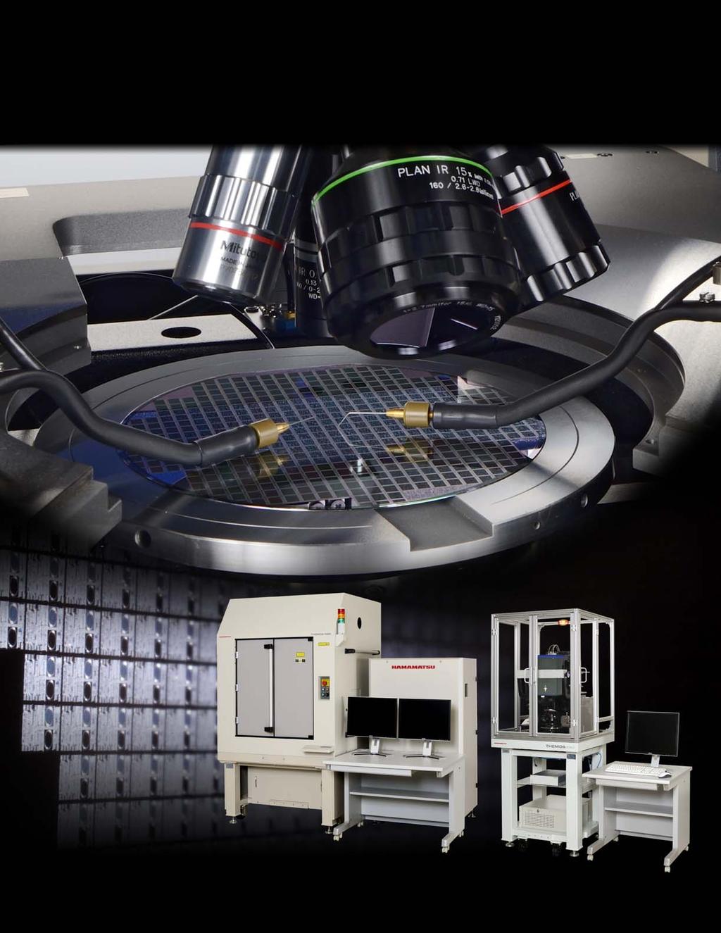
1 R series


2 5AHEAI New Highsensitivity detector thermal detector (InSb) Motorized turret with objective lenses Two objective lenses for analyzing thermal emissions Three objective lenses for probing and laser scanning The THEMOS series thermal emission microscope is a semiconductor failure analysis system that pinpoints failures by detecting thermal emissions generated within the semiconductor device. The increasing trend toward hyperfine patterns and lower supply voltages in semiconductor devices makes the infrared rays emitted by heat generated from semiconductor failure points fainter and more difficult to detect. The THEMOS series, which incorporates a highsensitivity InSb camera, has a flexible product lineup from a simple stand model to an advanced system with an IR confocal laser microscope. With this flexibility, the THEMOS series can test any device from PC boards to chips. Grinding Lead frame Thermal emissions Back side (Mirror polishing) Plastic mold Hot spot Bias Si substrate Pattern being measured Thermal emission analysis imaged through the backside Features High sensitivity is achieved by: InSb camera having high sensitivity in the 3 μm to 5 μm wavelength region Lens design optimized for 3 μm to 5 μm wavelengths Low noise using a lockin function () High cooling performance by a Stirling cycle cooler Noise equivalent temperature difference (NETD) is 20 mk. High resolution is achieved by: InSb camera with pixels (Pixel size: 15 μm) Superimposing a laser pattern image from the IR confocal laser microscope Thermal NanoLens is available. () High speed detection available by *windowing function Movie function Dynamic measurement available by tester link Flexible system structure for micro to macro observation User friendly operation identical to PHEMOS and μamos series Full lineup of optional features Applications Shortcircuit of metal wirings Abnormality of contact holes Microplasma leakage in oxide layer Oxide layer breakdown TFTLCD leakage / Organic EL leakage localization Observation of temperature abnormalities in devices under development process Temperature mapping of devices and PC boards *Windowing function Possible to measure a specific area with high frame rate. Region of interest Frame rate 640 pixels 512 pixels 100 Hz 320 pixels 256 pixels 200 Hz 160 pixels 128 pixels 400 Hz 64 pixels 32 pixels 1000 Hz 2


 High S/N is achieved by acquiring signals at a specific frequency and eliminating signals at")


3 Thermal lockin measurement Thermal lockin measurement The lockin measurement method deducts noise by synchronizing the timing of power supply to a device and image capture. With this method, a thermal lockin unit can provide high quality images even for low voltage devices. No lockin (S/N 4.4) Power Thermal emission ON ON ON OFF OFF OFF A B C D E F G A B C Acquired images Phase image Possible to localize a heat source by visualizing heat timing from phase images. D E F G 10 higher S/N Lockin (S/N 55.7) High S/N is achieved by acquiring signals at a specific frequency and eliminating signals at other frequencies as noise. Objective lens: 15, Bias: 1.0 V, 2.3 ma Amplitude image Phase image IR emission intensity map Heat timing map 1 IR emission: High Phase shift: Small 2 IR emission: Low Phase shift: Small 3 IR emission: Low Phase shift: Large 1 and 2 show small phase shift, which means fast heat timing. It indicates a heat source. 3 shows large phase shift, which indicates diffused heat. Image difference by frequency Possible to narrow down the heat source by increasing frequency. No lockin: 40 s Lockin: 1 Hz Lockin: 20 Hz 3


4 Thermal lockin measurement Measurement examples Case study: Package device observation Microprocessor Chip size: 30 mm 30 mm Superimposed the thermal image on an Xray image Case study: Defect layer observation by opening a side of a device Made a small opening at a side of mold to see a Si die. Side open area Lockin phase image at the opening area Measurement data 0.8 IR objective lens, 5 V, 1 Hz Measurement data 4 IR objective lens Case study: CMOS observation Found a defect under a bump Frontside observation Backside observation FIB cross section M1 M3 M2 M4 M5 M6 4 IR lens Si thickness 350 μm, 0.8 IR lens Peeling between M5 and M6 layers Case study: Wiring failure between a PCB and a packaged device Observed a heat source before opening the package. After opening the package, took phase images to narrow down the heat source. Amplitude image unopened package Phase image opened package 0.8 Lockin 5 Hz 0.8 Lockin 5 Hz Further observation by OBIRCH analysis pinpointed the heat source. Phase image opened package 4 Lockin 20 Hz OBIRCH 20 4

 PM8, PM8DSP PM8, PM8DSP Eyepiece for probing Lens for probing NIR 5 5 NIR 5 5 Antivibration table Dark box THEMOS analysis software")


5 Selection Micro / Macro type THEMOS1000 Flexible system structure corresponding to customer needs and application Simple and wide view type Prober type THEMOS mini System configurations Type THEMOS1000 THEMOS mini Micro / Macro type* 1 Simple and Prober type* wide view type* 1 1 C InSb camera IR confocal laser microscope Auto stage control XYZ Manual XYZ Z Manual Standard lens 0.8, 4, , 4, mm* 3, 0.8, 4, mm* 3 0.8, 4, 15 Sample stage PM8, PM8DSP HPK stage (8inch) PM8, PM8DSP PM8, PM8DSP Eyepiece for probing Lens for probing NIR 5 5 NIR 5 5 Antivibration table Dark box THEMOS analysis software FOV (unit: mm) to to , to < to Object Wafer (up to 12inch) Si die, Package PCB* 2, Wafer (up to 8inch) Si die, Package PCB, Wafer (up to 8inch) Si die, Package PCB, PV, LCD PCB* 2, Wafer (up to 8inch) Si die, Package : Standard : Not available * 1 : The systems are special order products. * 2 : In the case of integrating 0.29 objective lens * 3 : The lens for macro observation Functions Function THEMOS1000 THEMOS mini Micro / Macro type* 1 Simple and Prober type* wide view type* 1 1 Thermal lockin measurement 3DIC measurement Temperature measurement function Thermal nanolens Movie function Windowing function External triggering IROBIRCH analysis function DALS Photoemission analysis EO probing unit : Standard : Not available * 1 : The systems are special order products. 5


6 Overview of function 3DIC measurement function A12319 Possible to detect a heat point and its point of origin within stacked IC layers by using phase images taken by lockin measurement and calculating them with thermal property information of each layer. If a layer's material information is unknown, it is possible to obtain the information by using a pulse heater. Even with the obtained material information, depth can be measured within a few % error. Principle Heat point 1 Device Heat point 2 Heat point 1 Phase IRray Phase shift Heat source Heat point 2 Phase Heat generated from failure points 3DIC measurement software From the phase shift difference, the depth of a heat point is calculated. Indicate the depth of a heat point by the heat conductance algorithm and thermal property information of a device material Pulse heater Obtain thermal property information using a pulse heater. It is important to input the correct material information to get an accurate result. When you do not have the thermal property information of a material used in a device, it is possible to obtain that data by measuring the material with a pulse heater. Large phase shift (A heat spot is deep.) Small phase shift (A heat spot is close to the surface.) 3DIC MEASUREMENT FUNCTION Temperature measurement function U11389 By knowing the true temperature of a device under operation and feeding it back to the design process at an early stage, device verification time can be shortened as well as enhance product reliability. The function is also useful to observe temperature behavior which changes depending on operating environment. The measurement can be available easily by adding the U11389 temperature measurement function. Temperature image Note : Depending on measurement environment, structure of objects or material of objects, there is a case that measurement can't be carried out properly. Temperature Coordinates 6


 40 30 (THEMOS mini) 33 26 (THEMOS mini) 12 9.6 2.")
 0.8 0.")


 Output: 200 mw (CW), 800 mw (pulse) * Can't use 2 lasers of")


 A9771 Dynamic analysis by laser")

 changes due to heat generated by the laser.")


7 Overview of function Optics Objective lens Macro lens MWIR 0.24 : A MWIR 0.24 : A MWIR 0.29 MWIR 0.8 MWIR 4 MWIR 8 MWIR 15 MWIR 30 MPlanNIR 5 : A MPlanNIR 20 : A MPlanNIR 100 : A : Standard N.A WD (mm) FOV (mm) Macro analysis Newly developed 0.29 IR lens provides a clear wide view image without a narcissus phenomenon and shading. View size comparison (THEMOS1000) (THEMOS mini) (THEMOS mini) (THEMOS1000) (THEMOS1000) IR confocal laser scan microscope THEMOS1000 provides high resolution pattern images by integrating an IR confocal laser scan microscope. By overlaying a laser pattern image on a thermal image, heat point can be localized accurately. 1.3 μm Laser diode Output: 100 mw 1.3 μm High power laser (Option) Output: 400 mw or more 1.1 μm Pulse laser (Option) Output: 200 mw (CW), 800 mw (pulse) * Can't use 2 lasers of the same wavelength. IROBIRCH analysis function A8755 The highly popular IROBIRCH (Infrared Optical Beam Induced Resistance CHange) analysis function can be added as an option to detect line defects such as leakage or IDDQ defects. It is possible to measure at 4 quadrant voltage/current. Dynamic analysis by laser stimulation kit (DALS) A9771 Dynamic analysis by laser stimulation (DALS) is a new method to analyze device operation conditions by means of laser radiation. Stimulate a device with a 1.3 μm laser while operating it with test patterns by LSI tester. Then device operation status (pass/fail) changes due to heat generated by the laser. The pass/fail signal change is expressed as an image that indicates the point causing timing delay, marginal defect, etc. Thermal NanoLens System A11079 The Thermal NanoLens System provides drastic improvements in light correction efficiency and resolution by high N.A.. Microscope immersion oil applied between the sample and lens achieves high N.A. even on samples with poor surface flatness. A manipulator simplifies the NanoLens system design, making it easy to retrofit into your working equipment. 0.8 XYZ axis Magnification 3.49 N.A Standard objective lens Thermal NanoLens Back side 0.8 LSI tester docking Semiconductor devices are becoming ever more complicated, which makes it essential to interface with LSI testers to initialize sampling measurement and to set special conditions. Installing a dedicated probe card adapter allows cable docking with LSI testers to perform analysis. 7
 without changing sample setting. It saves you time and lab space. Type No.")
8 Overview of function/specifications Camera selection for photoemission observation A full lineup of optional cameras that detect faint photoemission from visible to near infrared light is available. Dual stage structure of THEMOS1000 allows twoimage acquisition (photoemission and thermal emission) without changing sample setting. It saves you time and lab space. Type No. InGaAs camera C InGaAs camera C InGaAs camera C Cooled CCD camera C SiCCD camera C Cooling type Liquid nitrogen cooling Peltier cooling Liquid nitrogen cooling Peltier cooling Peltier cooling Effective number of pixels 640 (H) 512 (V) 640 (H) 512 (V) 1000 (H) 1000 (V) 1024 (H) 1024 (V) 1024 (H) 1024 (V) Spectral sensitivity 900 nm to 1550 nm 900 nm to 1550 nm 900 nm to 1550 nm 300 nm to 1100 nm 400 nm to 1100 nm Laser marker C7638 Marking the vicinity of a localized failure point or four points around the failure point makes it easy to transfer position information on that failure point to other analysis equipment. EO Probing Unit C The EO Probing Unit is a tool to observe a transistor's status through the Si substrate using an incoherent light source. It is composed of the EOP (Electro Optical Probing) to measure operation voltage of a transistor rapidly and the EOFM (Electro Optical Frequency Mapping) to image active transistors at a specific frequency. Utility Line voltage Power consumption Vacuum Compressed air THEMOS1000 AC 220 V (50 Hz/60 Hz) 3000 VA Approx. 80 kpa or more 0.5 MPa to 0.7 MPa THEMOS mini AC 220 V (50 Hz/60 Hz) 700 VA Approx. 80 kpa or more 0.5 MPa to 0.7 MPa Dimensions/Weight (Including option) Dimensions/Weight THEMOS1000 main unit 1360 mm (W) 1410 mm (D) 2120 mm (H), Approx. 900 kg THEMOS control rack 880 mm (W) 700 mm (D) 1542 mm (H), Approx. 255 kg PC desk 1000 mm (W) 800 mm (D) 700 mm (H), Approx. 45 kg * Weight of THEMOS1000 main unit includes a prober or equivalent item. THEMOS mini main unit PC desk Dimensions/Weight 880 mm (W) 840 mm (D) 1993 mm (H), Approx. 450 kg 700 mm (W) 700 mm (D) 700 mm (H), Approx. 45 kg LASER SAFETY Hamamatsu Photonics classifies laser diodes, and provides appropriate safety measures and labels according to the classification as required for manufacturers according to IEC When using this product, follow all safety measures according to the IEC. CLASS Ι LASER PRODUCT Description Label (Sample) Caution Label THEMOS are registered trademark of Hamamatsu Photonics K.K. (France, Germany, Japan, U.K., U.S.A.) True Thermal are registered trademark of Hamamatsu Photonics K.K. (Eu, Japan, U.S.A.) Product and software package names noted in this documentation are trademarks or registered trademarks of their respective manufacturers. Information furnished by HAMAMATSU is believed to be reliable. However, no responsibility is assumed for possible inaccuracies or omissions. Specifications and external appearance are subject to change without notice Hamamatsu Photonics K.K. HAMAMATSU PHOTONICS K.K. HAMAMATSU PHOTONICS K.K., Systems Division 812 Jokocho, Higashiku, Hamamatsu City, , Japan, Telephone: (81) , Fax: (81) , export@sys.hpk.co.jp U.S.A.: Hamamatsu Corporation: 360 Foothill Road, Bridgewater, N.J 08807, U.S.A., Telephone: (1) , Fax: (1) usa@hamamatsu.com Germany: Hamamatsu Photonics Deutschland GmbH.: Arzbergerstr. 10, D82211 Herrsching am Ammersee, Germany, Telephone: (49) , Fax: (49) info@hamamatsu.de France: Hamamatsu Photonics France S.A.R.L.: 19, Rue du Saule Trapu, Parc du Moulin de Massy, Massy Cedex, France, Telephone: (33) , Fax: (33) infos@hamamatsu.fr United Kingdom: Hamamatsu Photonics UK Limited: 2 Howard Court,10 Tewin Road, Welwyn Garden City, Hertfordshire AL7 1BW, UK, Telephone: (44) , Fax: (44) info@hamamatsu.co.uk North Europe: Hamamatsu Photonics Norden AB: Torshamnsgatan Kista, Sweden, Telephone: (46) , Fax: (46) info@hamamatsu.se Italy: Hamamatsu Photonics Italia S.r.l.: Strada della Moia, 1 int Arese (Milano), Italy, Telephone: (39) , Fax: (39) info@hamamatsu.it China: Hamamatsu Photonics (China) Co., Ltd.: B1201 Jiaming Center, No.27 Dongsanhuan Beilu, Chaoyang District, Beijing , China, Telephone: (86) , Fax: (86) hpc@hamamatsu.com.cn Cat. No. SSMS0012E13 MAR/2014 HPK Created in Japan
WAFER PROBER MODEL. IR-OBIRCH analysis system Infra Red - Optical Beam Induced Resistance CHange AMOS -200
 WAFER PROBER MODEL IR-OBIRCH analysis system Infra Red - Optical Beam Induced Resistance CHange AMOS -200 IR-OBIRCH Analysis System The μamos is a semiconductor failure analysis system which uses IR-OBIRCH
-MP. Inverted emission microscope C
 Inverted emission microscope C10506-04-16 The iphemos inverted emission microscope is a semiconductor failure analysis system designed to identify failure locations by detecting the light and heat emitted
Emission Microscope. series
 R series Reveals Invisible Defects and Failures Detects very faint emissions caused by anomalies quickly and accurately to determine failure locations. The series of emission microscope is a group of semiconductor
IR-OBIRCH analysis system -1000
 IR-OBIRCH analysis system R Overview The μamos is a semiconductor failure analysis system which uses the IR-OBIRCH method for localization of leakage current paths and the abnormal resistance points in
Low bias operation, for 800 nm band
 Low bias operation, for 800 nm band These are 800 nm band near-infrared Si APDs that can operate at low voltages, 200 V or less. They are suitable for applications such as FSO (free space optics) and optical
Short wavelength type APD. Effective photosensitive area (mm) Effective photosensitive area size* 2
 Effective photosensitive area size* 2") Short wavelength type APD Features High sensitivity at visible range Low noise High gain Low capacitance Applications Low-light-level measurement Analytical instrument Structure / Absolute maximum ratings
Short wavelength type APD Features High sensitivity at visible range Low noise High gain Low capacitance Applications Low-light-level measurement Analytical instrument Structure / Absolute maximum ratings
InAsSb photovoltaic detector
 InAsSb photovoltaic detector P12691-21 High-speed response and high sensitivity in the 8 μm spectral band Thermoelectrically cooled infrared detector with no liquid nitrogen required The P12691-21 is an
Effective photosensitive area. Photosensitive area size
 High performance, high reliability Si PIN photodiodes The is a high-speed Si PIN photodiode having high sensitivity over a wide spectral range from visible to near infrared light. The provides high performance
Photosensitive area size (mm) Reverse voltage VR max (V) R to +60
 Reverse voltage VR max (V) R to +60") ,, 6 to 37 mm resistance length PSD for precision distance measurement Hamamatsu provides various types of one-dimensional PSD (position sensitive detector) designed for precision distance measurement
,, 6 to 37 mm resistance length PSD for precision distance measurement Hamamatsu provides various types of one-dimensional PSD (position sensitive detector) designed for precision distance measurement
Peak emission wavelength: 3.9 μm
 Peak emission wavelength: 3.9 μm The is a high-output mid-infrared LED with a 3.9 µm peak emission wavelength. It is a product that has been achieved using Hamamatsu unique crystal growth technology and
MPPC (Multi-Pixel Photon Counter)
") S13362-35DG Significantly reduced crosstalk, low afterpulses The can reduce dark count by cooling in addition to low afterpulses and low crosstalk of the S1336 series. The integrates the S1336 series with
S13362-35DG Significantly reduced crosstalk, low afterpulses The can reduce dark count by cooling in addition to low afterpulses and low crosstalk of the S1336 series. The integrates the S1336 series with
Application OCT. Dimensions (mm) Weight (g) Operating temperature* 1 Storage temperature* 1 λ=1.55 μm (V) (mw)
 Weight (g) Operating temperature* 1 Storage temperature* 1 λ=1.55 μm (V) (mw)") Balanced detectors with reduced multiple reflections These are differential amplification type photoelectric conversion modules containing two Hamamatsu photodiodes with balanced characteristics. The photodiodes
Balanced detectors with reduced multiple reflections These are differential amplification type photoelectric conversion modules containing two Hamamatsu photodiodes with balanced characteristics. The photodiodes
Optics modules. Absorbance measurement module with built-in photodiode array, optical elements, current-tovoltage. C13398 series.
 Absorbance measurement module with built-in photodiode array, optical elements, current-tovoltage converter, etc. The is an optics module for absorbance measurement featuring high blocking performance
InGaAs multichannel detector head
 Near infrared line camera (Line rate: 31.25 khz) The is a multichannel detector head suitable for applications where high-speed response is required, such as SD- OCT (spectral domain-optical coherence
InAsSb photovoltaic detectors
 High-speed response and high sensitivity in the spectral band up to 11 μm Infrared detectors The are photovoltaic type infrared detectors that have achieved high sensitivity in the spectral band up to
Driver circuits for CCD image sensor
 Driver circuit for CCD image sensor (S10420/S11071/S11510 series) The and are driver circuits designed for HAMAMATSU CCD image sensor S10420/S11071/S11510 series. The and can be used in spectrometer when
InAsSb photovoltaic detector
 InAsSb photovoltaic detector P2-2 High-speed response and high sensitivity in the 5 μm spectral band Thermoelectrically cooled infrared detector with no liquid nitrogen required The P2-2 is an infrared
Driver circuit for InGaAs linear image sensor
 Driver circuit for InGaAs linear image sensor [G11620 series (non-cooled type)] The is a driver circuit developed for InGaAs linear image sensors [G11620 series (non-cooled type)]. The driver circuit consists
All-in-one solutions For applications with imaging challenges, we offer a wide range of TDI solutions.
 Speed Sensitivity Resolution All-in-one solutions For applications with imaging challenges, we offer a wide range of solutions. high-throughput Imaging in Low Light Applications New Generation of Solves
MPPC modules. MPPC array modules for very-low-level light detection, 16 ch analog output. C13368/C13369 series (Analog output type)
") MPPC modules C13368/C13369 series (Analog output type) MPPC array modules for very-low-level light detection, 16 ch analog output The C13368/C13369 series (analog output type) is an optical measurement
MPPC modules C13368/C13369 series (Analog output type) MPPC array modules for very-low-level light detection, 16 ch analog output The C13368/C13369 series (analog output type) is an optical measurement
Accessories for infrared detector
 Temperature controllers Heatsinks for TE-cooled detector Chopper, etc. Wide lineups of accessories for infrared detector HAMAMATSU provides temperature controllers, heatsinks for TE-cooled detector, chopper
Driver circuit for InGaAs linear image sensor
 (G11135 series, G14006-512DE) The is a driver circuit developed for InGaAs linear image sensors (G11135 series, G14006-512DE). The driver circuit consists of an analog video signal processing circuit (16-bit
PbSe photoconductive detectors
 PbSe photoconductive detectors P9696 series P327-8 Infrared detectors with fast response and high sensitivity in 5 μm wavelength band Compared to other detectors used in the same wavelength regions, PbSe
Photon counting module
 Photon counting module Fiber coupling type, low-light-level detection The is a photon counting module that can detect low-level light. It consists of a TE-cooled single pixel photon counter (SPPC), signal
Effective photosensitive area (mm)
") Chip carrier package for mount The, S5107, and S7510 are Si PIN photodiodes sealed in chip carrier packages suitable for mount using automated solder reflow techniques. These photodiodes have large photosensitive
Chip carrier package for mount The, S5107, and S7510 are Si PIN photodiodes sealed in chip carrier packages suitable for mount using automated solder reflow techniques. These photodiodes have large photosensitive
NMOS linear image sensor
 Image sensor highly sensitive to X-rays from 0 k to 00 kev s are self-scanning photodiode arrays designed specifically as detectors for multichannel spectroscopy. The scanning circuit is made up of N-channel
1-D PSD with small plastic package
 1D PSD with small plastic package Hamamatsu offers a variety of 1D PSDs (position sensitive detectors) molded into plastic packages. These PSDs feature excellent position detection resolution, high resistance
Driver circuit for CCD linear image sensor
 For CCD image sensor (S11151-2048) The is a driver circuit designed for Hamamatsu CCD image sensor S11151-2048. The can be used in spectrometers when combined with the S11151-2048. The holds a CCD driver
InGaAs PIN photodiode arrays
 16/32/46 element InGaAs array for near IR detection The is one-dimensional InGaAs PIN photodiode array in a ceramic DIP (dual inline package). It can be used to perform simple spectroscopic analysis. Features
MPPC (multi-pixel photon counter)
") MPPC (multi-pixel photon counter) Low afterpulses, wide dynamic range, for high-speed measurement Photosensitive area: 1 1 mm These MPPCs utilize very small pixels arrayed at high densities to achieve
MPPC (multi-pixel photon counter) Low afterpulses, wide dynamic range, for high-speed measurement Photosensitive area: 1 1 mm These MPPCs utilize very small pixels arrayed at high densities to achieve
Peak emission wavelength: 4.3 μm
 Peak emission wavelength: 4.3 μm The is a mid infrared LED with a 4.3 μm peak emission wavelength. It is a product that has been achieved using Hamamatsu unique crystal growth technology and process technology.
Effective photosensitive* 2 area size. Storage temperature Tstg (mm) ( C) ( C) S φ0.2 φ0.5 S φ to to +100 S9075
 ( C) ( C) S φ0.2 φ0.5 S φ to to +100 S9075") /-05/-10, S5344, S5345 Short wavelength type APD, for 600 nm band These are short wavelength APDs with improved sensitivity in the UV to visible range. They offer high gain, high sensitivity, and low noise
/-05/-10, S5344, S5345 Short wavelength type APD, for 600 nm band These are short wavelength APDs with improved sensitivity in the UV to visible range. They offer high gain, high sensitivity, and low noise
UV-LED MODULE. UV Irradiation Intensity Distribution Graphs
 UV-LED MODULE UV Irradiation Intensity Distribution Graphs Product Lineup Lens Lineup Product Lineup LED DRIVER C1559-1 LED HEAD UNIT L1561/L196 SERIES standard type standard type high power type high
Driver circuit for MPPC
 Simple evaluation starter kit for non-cooled s The is a starter kit designed for simple non-cooled evaluations. It consists of a sensor board and a power supply board. The sensor board includes an socket
Parameter Symbol Specification Unit Photosensitive area - ɸ0.8 mm Package mm
 Surface mount type, high-speed Si photodiode The is a Si PIN photodiode with sensitivities in the visible to near infrared range and is compatible with lead-free solder reflow. It features high-speed response
InAsSb photovoltaic detectors
 High-speed response and high sensitivity in the spectral band up to 5 μm Infrared detectors The are photovoltaic type infrared detectors that have achieved high sensitivity in the spectral band up to 5
Driver circuit for CMOS linear image sensor
 Driver circuit for CMOS linear image sensor C13015-01 For CMOS linear image sensor S11639-01, etc. The C13015-01 is a driver circuit developed for Hamamatsu CMOS linear image sensor S11639-01, etc. By
These Si photodiodes have sensitivity in the UV to near IR range. They are suitable for low-light-level detection in analysis and the like.
 UV to near IR for precision photometry These Si photodiodes have sensitivity in the UV to near IR range. They are suitable for low-light-level detection in analysis and the like. Features High sensitivity
MCT photoconductive detectors
 Non-cooled type and suitable for long, continuous operation Features Choice of spectral response (up to 12 μm) The band gap can be adjusted by controlling the composition ratio of HgTe and CdTe. Utilizing
Infrared detector modules with preamp
 Easy-to-use detector modules with built-in preamps Infrared detector modules operate just by connecting to DC power supplies. The detector element is selectable from among InGaAs, InAs, InSb, and InAsSb
Suppressed IR sensitivity
 For UV to visible, precision photometry; suppressed IR sensitivity These Si photodiodes have suppressed IR sensitivity. They are suitable for low-light-level detection in analysis and the like. Features
MCT photoconductive detectors
 MCT photoconductive detectors P3257 series P4249-08 0 μm band infrared detector with high sensitivity and high-speed response Features High-speed response, high sensitivity in the 0 μm band detection Photoconductive
Si PIN photodiodes. High-speed detectors with plastic package. Structure. Absolute maximum ratings
 High-speed detectors with plastic package The and are high-speed APC (auto power control) detectors developed for monitoring laser diodes with a peak wavelength of 66 nm or 78 nm. The is designed for surface
M=100, RL=50 Ω λ=800 nm, -3 db
 Low bias operation, for 800 nm band, small package Features Miniature and thin package:.8 3..0 t mm Stable operation at low bias High-speed response High sensitivity Low noise Applications Optical rangefinder
Photo IC diode. Plastic package shaped the same as metal package. S SB. Features. Applications
 Plastic package shaped the same as metal package The photo IC has spectral response close to human eye sensitivity. Two photosensitive areas are made on a single chip. Almost only the visible range can
Effective photosensitive area (mm) Photosensitive area size
 Photosensitive area size") High UV resistance, photodiodes for UV monitor The are Si photodiodes that have achieved high reliability for monitoring ultraviolet light by employing a structure that does not use resin. They exhibit
High UV resistance, photodiodes for UV monitor The are Si photodiodes that have achieved high reliability for monitoring ultraviolet light by employing a structure that does not use resin. They exhibit
Photosensor with front-end IC
 Compact APD suitable for various light level detection The is a compact optical device that integrates a Si APD and preamp. It has a built-in DC feedback circuit for reducing the effects of background
APD modules. APD module integrated with peripheral circuits. C12703 series. Selection guide. Block diagram
 APD module integrated with peripheral circuits Features Uses a high sensitivity APD Two types of APDs with different photosensitive areas (φ1.5 mm, φ3. mm) are provided. On-board high sensitivity circuit
APD modules. Operates an APD with single 5 V supply (standard type, short-wavelength type) C12702 series.
 C12702 series.") Operates an APD with single 5 V supply (standard type, short-wavelength type) Features Includes a high-sensitivity APD Uses a Hamamatsu high-sensitivity Si APD. Four types are available with different
Operates an APD with single 5 V supply (standard type, short-wavelength type) Features Includes a high-sensitivity APD Uses a Hamamatsu high-sensitivity Si APD. Four types are available with different
Peak sensitivity wavelength λp (nm) Photosensitive area (mm)
 Photosensitive area (mm)") Integrates a -PSD for precision photometry or a 4-segment Si photodiode with low-noise amp in a compact case PSD modules contain a high-precision two-dimensional PSD (position sensitive detector) or a
Integrates a -PSD for precision photometry or a 4-segment Si photodiode with low-noise amp in a compact case PSD modules contain a high-precision two-dimensional PSD (position sensitive detector) or a
16-element Si photodiode arrays
 Back-illuminated photodiode arrays for X-ray nondestructive inspection (element pitch: mm) The is a back-illuminated type 16-element photodiode array specifically designed for non-destructive X- ray inspection.
Si PIN photodiodes. High-speed detectors with plastic package. Structure. Absolute maximum ratings
 High-speed detectors with plastic package The and are high-speed APC (auto power control) detectors developed for monitoring laser diodes with a peak wavelength of 66 nm or 78 nm. The is designed for surface
16-element Si photodiode arrays
 Back-illuminated photodiode arrays for X-ray nondestructive inspection (element pitch: mm) The is a back-illuminated type 16-element photodiode array specifically designed for non-destructive X-ray inspection.
Non-discrete position sensors utilizing photodiode surface resistance
 Twodimensional PSD Nondiscrete position sensors utilizing photodiode surface resistance PSD (position sensitive detector) is an optoelectronic position sensor utilizing photodiode surface resistance. Unlike
Reverse voltage VR max. Electrical and optical characteristics (Typ. Ta=25 C, unless otherwise noted) Short. Temp. S coefficient (A/W) of
 Short. Temp. S coefficient (A/W) of") Ceramic package photodiodes with low dark current The are ceramic package photodiodes that offer low dark current. Ceramic package used is light-impervious, so no stray light can reach the photosensitive
Ceramic package photodiodes with low dark current The are ceramic package photodiodes that offer low dark current. Ceramic package used is light-impervious, so no stray light can reach the photosensitive
Signal processing circuit for 2-D PSD
 Signal processing circuit for 2-D PSD Circuit board for easier 2-D PSD operation The is a DC signal processing circuit for two-dimensional PSD. It is suitable for displacement measurements using DC light.
New product of near infrared (to 900 nm) detection
 detection") WITH THERMOELECTRIC COOLER H7844 New product of near infrared (to 900 nm) detection FEATURES A newly developed high sensitivity multialkali side-on photomultiplier tube Fast cooling (3 minutes) by thermoelectric
WITH THERMOELECTRIC COOLER H7844 New product of near infrared (to 900 nm) detection FEATURES A newly developed high sensitivity multialkali side-on photomultiplier tube Fast cooling (3 minutes) by thermoelectric
Photosensitive area (mm) 4 4. Peak sensitivity wavelength (nm) Supply voltage Dark state. Max. Vcc max. Tstg Min. Max. (ma) (V)
 4 4. Peak sensitivity wavelength (nm) Supply voltage Dark state. Max. Vcc max. Tstg Min. Max. (ma) (V)") Integrates a PSD for precision photometry or a 4-segment Si photodiode with low-noise amp in a compact case PSD modules contain a high-precision two-dimensional PSD (position sensitive detector) or a 4-segment
Integrates a PSD for precision photometry or a 4-segment Si photodiode with low-noise amp in a compact case PSD modules contain a high-precision two-dimensional PSD (position sensitive detector) or a 4-segment
Applications. Photosensitive area size. Storage temperature Tstg (mm) (mm 2 ) (V) ( C) ( C) S
 (mm 2 ) (V) ( C) ( C) S") , etc. Photodiodes molded into clear plastic packages These are Si photodiodes molded into clear plastic packages. Two types are available with sensitivity in the visible range and in the visible to near
, etc. Photodiodes molded into clear plastic packages These are Si photodiodes molded into clear plastic packages. Two types are available with sensitivity in the visible range and in the visible to near
Signal processing circuit for 1-D PSD
 Signal processing circuit for 1-D PSD Circuit board for easier 1-D PSD operation The is a DC signal processing circuit for one-dimensional PSD. It is suitable for displacement measurements using DC light.
Photo IC diode. Plastic package shaped the same as metal package. S SB. Absolute maximum ratings (Ta=25 C)
") Plastic package shaped the same as metal package The photo IC has spectral response close to human eye sensitivity. Two photosensitive areas are made on a single chip. Almost only the visible range can
Plastic package shaped the same as metal package The photo IC has spectral response close to human eye sensitivity. Two photosensitive areas are made on a single chip. Almost only the visible range can
Driver circuit for CCD linear image sensor
 Driver circuit for CCD linear image sensor C11165-02 For CCD image sensor (S11155/S11156-2048-02) The C11165-02 is a driver circuit designed for Hamamatsu CCD image sensor S11155/S11156-2048-02. The C11165-02
LCOS-SLM (Liquid Crystal on Silicon - Spatial Light Modulator)
") POWER LCOS-SLM CONTROLLER RESET POWER OUTPUT ERROR LCOS-SLM (Liquid Crystal on Silicon - Spatial Light Modulator) Control your light! Shape your beam! Improve your image! The devices are a reflective type
POWER LCOS-SLM CONTROLLER RESET POWER OUTPUT ERROR LCOS-SLM (Liquid Crystal on Silicon - Spatial Light Modulator) Control your light! Shape your beam! Improve your image! The devices are a reflective type
Power supply for MPPC
 Power supply for MPPC C1104-0 Bias power supply with built-in high precision temperature compensation for MPPCs The C1104-0 is a high voltage power supply that is optimized for MPPCs (multi-pixel photon
Driver circuit for CCD image sensor
 For CCD image sensor S11850-1106, S11511 series The is a driver circuit developed for CCD image sensors S11850-1106 and S11511 series. By connecting the to a PC through the USB 2.0 interface, you can use
RGB color sensor. Effective photosensitive area. Green, Red: 2.25 Blue : 4.5
 Si photodiodes S6428-01 S6429-01 S6430-01 RGB color sensor The S6428-01, S6429-01 and S6430-01 are color sensors designed to respectively detect monochromatic colors of blue (λp=460 nm), green (λp=540
Mini-spectrometer. SMD series C14384MA-01. High sensitivity in the near infrared region (to 1050 nm), ultra-compact grating type spectrometer
, ultra-compact grating type spectrometer") Mini-spectrometer SMD series C14384MA-01 High sensitivity in the near infrared region (to 1050 nm), ultra-compact grating type spectrometer The C14384MA-01 is a ultra-compact grating type spectrometer
Mini-spectrometer SMD series C14384MA-01 High sensitivity in the near infrared region (to 1050 nm), ultra-compact grating type spectrometer The C14384MA-01 is a ultra-compact grating type spectrometer
MPPC (Multi-Pixel Photon Counter)
") MPPC (Multi-Pixel Photon Counter) MPPCs in a chip size package miniaturized through the adoption of TSV structure The are MPPCs for precision measurement miniaturized by the use of TSV (through-silicon
MPPC (Multi-Pixel Photon Counter) MPPCs in a chip size package miniaturized through the adoption of TSV structure The are MPPCs for precision measurement miniaturized by the use of TSV (through-silicon
Mini-spectrometer. TF series. Compact and thin, built-in high-sensitivity CMOS image sensor for Raman spectroscopy C14214MA. Applications.
 TF series C14214MA Compact and thin, built-in high-sensitivity CMOS for Raman spectroscopy The mini-spectrometer TF series is a polychromator provided in a compact, thin case that houses optical elements,,
Parameter Specification Unit Photosensitive area mm Package Glass epoxy - Seal material Silicone resin -
 COB type, applicable to lead-free solder reflow The is a for visible to near infrared range and is compatible with lead-free solder reflow processes. The small and thin leadless package allows reducing
Photo IC for optical switch
 Photo IC with optical switch functions The S6841 and S8119 are specifically designed for optical switches. A transmission mode or reflection mode optical switch can be easily configured when used in combination
High-speed photodiodes (S5973 series: 1 GHz)
") S5973 series High-speed photodiodes (S5973 series: 1 GHz), and S5973 series are high-speed Si PIN photodiodes designed for visible to near infrared light detection. These photodiodes provide wideband characteristics
S5973 series High-speed photodiodes (S5973 series: 1 GHz), and S5973 series are high-speed Si PIN photodiodes designed for visible to near infrared light detection. These photodiodes provide wideband characteristics
Driver circuit for CCD linear image sensor
 Driver circuit for CCD linear image sensor C11165-01 For CCD image sensor (S11155/S11156-2048-01) The C11165-01 is a driver circuit designed for HAMAMATSU CCD image sensor S11155/S11156-2048-01. The C11165-01
mini-spectrometer TG series Long-wavelength type (to 2.55 μm) nearinfrared C11118GA Optical characteristics (Ta=25 C)
 nearinfrared C11118GA Optical characteristics (Ta=25 C)") Long-wavelength type (to 2.55 μm) nearinfrared mini-spectrometer Hamamatsu mini-spectrometers are polychromators integrated with optical elements and an. Light to be measured is guided into the entrance
Long-wavelength type (to 2.55 μm) nearinfrared mini-spectrometer Hamamatsu mini-spectrometers are polychromators integrated with optical elements and an. Light to be measured is guided into the entrance
Parameter Specification Unit Photosensitive area mm Package Glass epoxy - Seal material Epoxy resin -
 COB type, applicable to lead-free solder reflow The is a Si PIN photodiode for visible to near infrared range and is compatible with lead-free solder reflow processes. The small and thin leadless package
Photo IC diode. Wide operating temperature: -40 to +105 C. S MT. Absolute maximum ratings (Ta=25 C)
") Wide operating temperature: -40 to +05 C The photo IC has a spectral response close to human eye sensitivity. Two active areas are made on a single chip. Almost only the visible range can be measured by
Wide operating temperature: -40 to +05 C The photo IC has a spectral response close to human eye sensitivity. Two active areas are made on a single chip. Almost only the visible range can be measured by
Signal processing circuit for 2-D PSD
 Signal processing circuit for 2-D PSD Circuit board for easier 2-D PSD operation The is a DC signal processing circuit for two-dimensional PSD. It is suitable for displacement measurements using DC light.
FT series. Spectral response range 790 to 920 nm Spectral resolution Typ. 0.4 nm
 FT series C1354MA Compact and thin, built-in high-sensitivity CMOS for Raman spectroscopy The mini-spectrometer FT (flat type) series is a polychromator provided in a compact, thin case that houses optical
Mini-spectrometer. TM series. Trigger function and a high sensitivity CMOS image sensor included. C11697MB. Optical characteristics
 Trigger function and a high sensitivity CMOS included The is a polychromator integrated with optical elements, an and a driver circuit. Light to be measured is guided into the entrance port of through
Near infrared image sensor (0.9 to 1.7 µm) with high-speed data rate
 with high-speed data rate") IMAGE SENSOR InGaAs linear image sensor G99-56D/-5D Near infrared image sensor (.9 to.7 µm) with high-speed data rate HAMAMATSU provides high-speed, near infrared image sensors designed for detectors used
IMAGE SENSOR InGaAs linear image sensor G99-56D/-5D Near infrared image sensor (.9 to.7 µm) with high-speed data rate HAMAMATSU provides high-speed, near infrared image sensors designed for detectors used
Power supply for MPPC
 Power supply for MPPC C1104-0 Bias power supply with built-in high precision temperature compensation for MPPCs The C1104-0 is a high voltage power supply that is optimized for MPPCs (multi-pixel photon
16-element Si photodiode arrays
 S11212-421 S11212-321 S11212-021 S11212-121 Back-illuminated photodiode arrays for non-destructive inspection The is a back-illuminated type 16-element photodiode array specifically designed for non-destructive
Signal processing circuit for 1-D PSD
 Signal processing circuit for 1-D PSD Circuit board for easier 1-D PSD operation The is a DC signal processing circuit for one-dimensional PSD. It is suitable for displacement measurements using DC light.
Si photodiode. Applicable to lead-free solder reflow and wide temperature range. S9674. Absolute maximum ratings
 Applicable to lead-free solder reflow and wide temperature range The is a photodiode that is applicable to lead-free solder reflow and has an extremely wide operating and storage temperature range (-40
16-element Si photodiode arrays
 S11299-321 S11299-421 S11299-21 S11299-121 Back-illuminated photodiode arrays for X-ray non-destructive inspection, slender board type The is a back-illuminated type 16-element photodiode array specifically
TM series TM-UV/VIS-MOS
 C12MD C13MD For UV to near IR, integrating optical system, and circuit mini-spectrometers are polychromators integrated with optical elements, an and a driver circuit. Two models are available: C12MD (TM-UV/VIS-MOS)
TM series. Trigger function included
 Trigger function included The is a polychromator integrated with optical elements, an and a driver circuit. Light to be measured is guided into the entrance port of through an optical fiber and the spectrum
Mini-spectrometer. TG series. Enhanced near infrared sensitivity type. C9405CB. High sensitivity in near infrared region
 Enhanced near infrared sensitivity type The is a polychromator integrated with optical elements, an and a driver circuit. Light to be measured is guided into the entrance port of through an optical fiber
Driver circuit for CMOS linear image sensor
 High-precision driver circuit with variable integration time function The is a driver circuit specifically designed for the Hamamatsu S10111 to S10114 series, S10121 to S10124 series (-01) current-output
Photodiode modules. C10439 series. Integrates photodiode for precision photometry with low-noise amp.
 Integrates photodiode for precision photometry with low-noise amp The photodiode modules are high-precision photodetectors that integrate a photodiode and a current-to-voltage amplifier. The output from
Between elements measure. Photosensitive area (per 1 element)
") 16, 35, 46 element Si photodiode array for UV to NIR The are Si photodiode linear array mounted in ceramic DIPs (Dual Inline Packages). These photodiode arrays are primarily developed for low-light-level
16, 35, 46 element Si photodiode array for UV to NIR The are Si photodiode linear array mounted in ceramic DIPs (Dual Inline Packages). These photodiode arrays are primarily developed for low-light-level
Photo IC diode. COB (chip on board) type, small package. S CT. Absolute maximum ratings
 type, small package. S CT. Absolute maximum ratings") COB (chip on board) type, small package mm The photo IC has spectral response close to human eye sensitivity. Two photosensitive areas are made on a single chip. Almost only the visible range can be measured
COB (chip on board) type, small package mm The photo IC has spectral response close to human eye sensitivity. Two photosensitive areas are made on a single chip. Almost only the visible range can be measured
S P. Ultra-miniature, high performance Electromagnetically driven laser scanning MEMS mirror. Features.
 Si MEMS photodiode mirror Ultra-miniature, high performance Electromagnetically driven laser scanning MEMS mirror The is an electromagnetically driven mirror that incorporates our unique MEMS (micro-electro-mechanical
Variable gain and stable detection even at high gains
 MODULE APD module C5 Variable gain and stable detection even at high gains Along with an APD, current-to-voltage conversion circuit, and high-voltage power supply circuit, the C5 contains a microcontroller
Driver circuits for photodiode array with amplifier
 C98 series Compact, easytouse driver circuit The C98 series CMOS driver circuit is designed for photodiode arrays with amplifier. The C98 series operates a linear image sensor by just inputting two signals
Mini-spectrometer. TG series. Enhanced near infrared sensitivity type. C9405CB. High sensitivity in near infrared region
 Enhanced near infrared sensitivity type The is a polychromator integrated with optical elements, an and a driver circuit. Light to be measured is guided into the entrance port of through an optical fiber
Mini-spectrometers. TG series. High sensitivity type (integrated with backthinned type CCD image sensor) Optical characteristics
 Optical characteristics") H High sensitivity type (integrated with backthinned type ) mini-spectrometers are polychromators integrated with optical elements, an and a driver circuit. Light to be measured is guided into the entrance
H High sensitivity type (integrated with backthinned type ) mini-spectrometers are polychromators integrated with optical elements, an and a driver circuit. Light to be measured is guided into the entrance
Mini-spectrometers. TM series. High sensitivity type (integrated with backthinned type CCD image sensor) C10082CA/C10083CA series
 C10082CA/C10083CA series") C12CA/C1CA series type (integrated with backthinned type CCD ) mini-spectrometers are polychromators integrated with optical elements, an and a driver circuit. Light to be measured is guided into the entrance
C12CA/C1CA series type (integrated with backthinned type CCD ) mini-spectrometers are polychromators integrated with optical elements, an and a driver circuit. Light to be measured is guided into the entrance
Mini-spectrometer. TG series. For near IR, integrating optical system, image sensor and circuit. C9406GC, C9913GC, C9914GB
 , C9913GC, For near IR, integrating optical system, and circuit HAMAMATSU mini-spectrometers are polychromators integrated with optical elements and an. Light to be measured is guided into the entrance
MPPC modules. Photon counting module with built-in MPPC. C series C10751 series. Selection guide
 C10507-11 series C10751 series Photon counting module with built-in MPPC The MPPC (multi-pixel photon counter) module is a photon counting module capable of low-light-level detection. This module consists