Vertical Field Switching Blue Phase Liquid Crystals For Field Sequential Color Displays
|
|
|
- Susanna Bishop
- 6 years ago
- Views:
Transcription


1 University of Central Florida Electronic Theses and Dissertations Doctoral Dissertation (Open Access) Vertical Field Switching Blue Phase Liquid Crystals For Field Sequential Color Displays 2012 Hui-Chuan Cheng University of Central Florida Find similar works at: University of Central Florida Libraries Part of the Electromagnetics and Photonics Commons, and the Optics Commons STARS Citation Cheng, Hui-Chuan, "Vertical Field Switching Blue Phase Liquid Crystals For Field Sequential Color Displays" (2012). Electronic Theses and Dissertations. Paper This Doctoral Dissertation (Open Access) is brought to you for free and open access by STARS. It has been accepted for inclusion in Electronic Theses and Dissertations by an authorized administrator of STARS. For more information, please contact
2 VERTICAL FIELD SWITCHING BLUE PHASE LIQUID CRYSTALS FOR FIELD SEQUENTIAL COLOR DISPLAYS by HUI-CHUAN CHENG B.S. National Taiwan University, Taiwan, 2000 M.S. National Taiwan University, Taiwan, 2005 A dissertation submitted in partial fulfillment of the requirements for the degree of Doctor of Philosophy in the College of Optics and Photonics at the University of Central Florida Orlando, Florida Fall Term 2012 Major Professor: Shin-Tson Wu
3 2012 Hui-Chuan Cheng ii
4 ABSTRACT Low power consumption is a critical requirement for all liquid crystal display (LCD) devices. A field sequential color (FSC) LCD was proposed by using red (R), green (G) and blue (B) LEDs and removing the lossy component of color filters which only transmits ~30% of the incoming white light. Without color filters, FSC LCDs exhibit a ~3X higher optical efficiency and 3X higher resolution density as compared to the conventional color filters-based LCDs. However, color breakup (CBU) is a most disturbing defect that degrades the image quality in FSC displays. CBU can be observed in stationary or moving images. It manifests in FSC LCDs when there is a relative speed between the images and observers eyes, and the observer will see the color splitting patterns or rainbow effect at the boundary between two different colors. In Chapter 2, we introduce a five-primary display by adding additional yellow(y) and cyan(c) colors. From the analysis and simulations, five primaries can provide wide color gamut and meanwhile the white brightness is increased, as compared to the three-primary. Based on the five-primary theorem, we propose a method to reduce CBU of FSC LCDs by using RGBYC LEDs instead of RGB LEDs in the second section. Without increasing the sub-frame rate as three-primary LCDs, we can reduce the CBU by utilizing proper color sequence and weighting ratios. In addition, the color gamut achieves 140% NTSC and the white brightness increases by more than 13%, as compared to the three-primary FSC LCDs. Another strategy to suppress CBU is using higher field frequency, such as 540 Hz or even up to 1000 Hz. However, this approach needs liquid crystals with a very fast response time (<1 ms). Recently, the polymer-stabilized blue-phase liquid crystal (PS-BPLC) draws great attentions iii
5 because of improved temperature range which enables the applications for photonic devices and displays. PS-BPLC is a good candidate for FSC LCDs because of its submillisecond gray-to-gray response time, no need for alignment layer, and isotropic dark state. So far, almost all the BPLC devices utilize planar or protruded in-plane switching (IPS) electrode configuration. The structure of planar IPS is relatively simple, but the operating voltage is too high for thin-film transistor (TFT) addressing. Moreover, high voltage causes deformation of polymer network and induces a noticeable hysteresis. Protruded IPS is helpful for lowering the operating voltage, but the manufacturing process becomes more sophisticated. In Chapter 3, we propose a vertical field switching (VFS) mode for blue phase LCDs. The simple structure of VFS cell generates uniform vertical fields on the BPLC materials. From our experimental results, the operation voltage can be reduced to ~10V rms while eliminating the hysteresis. We also defined a critical field below which hysteresis does not occur. Above critical field, lattice distortion and other irreversible phase transition processes would occur. As a result, the associated response time would be slower. Therefore, VFS mode also shows faster response time than IPS mode. The operating voltage can be further reduced by choosing an optimized cell gap and a larger oblique incident angle in VFS blue phase LCDs. In Chapter 4, we propose several compensation mechanisms to improve the viewing angle of VFS blue-phase LCDs. The compensation principles are analyzed and simulation results evaluated. Because VFS blue-phase LCD processes several advantages over IPS blue-phase LCD and conventional LCDs, it could become a strong contender for next-generation display technology. iv
6 ACKNOWLEDGMENTS I would like to express my gratitude to those who have made contributions to this work and who have offered help during my study and research. Thank my advisor Prof. Shin-Tson Wu for his guidance, encouragement, and patience in the past few years. I also appreciate all the help from Prof. Wu s wife. The time staying in Orlando has become the best memory in my life. I am grateful to my committee members Prof. Patrick L. LiKamWa, Prof. Winston V. Schoenfeld, and Prof. Thomas X. Wu for their support and valuable comments. I would also like to thank my outstanding colleagues in the photonics and display group for their discussions, inspirations, and assistance in my research. I treasure the opportunity to work in such a great family led by Prof. Wu. Moreover, I would like to thank Chi-Mei Optoelectronics (CMO) (Taiwan), Industrial Technology Research Institute (ITRI) (Taiwan), and AU Optronics (AUO) (Taiwan) for their financial support of my research at University of Central Florida. Finally and most importantly, I want to thank my parents and sister in Taiwan for their support and the love they have shown all throughout my life. v
7 TABLE OF CONTENTS LIST OF FIGURES... viii LIST OF TABLES... xii CHAPTER 1: MULTI-PRIMARY COLOR DISPLAY Introduction of Liquid Crystal Display Multi-Primary Colors Introduction Principles and Simulations Five-Primary LCDs and Comparison Summary CHAPTER 2: FIELD SEQUENTIAL COLOR DISPLAY Introduction Color Breakup Multi-Primary FSC LCDs Discussions and Conclusions CHAPTER 3: BLUE PHASE LIQUID CRYSTAL DISPLAYS Blue Phase Liquid Crystal Introduction Planar In-Plane Switching BPLCD vi
8 3.2 Reducing Voltage for Blue Phase Liquid Crystal Display Vertical Field Switching BPLCD Device Structure Experiments and Simulations Summary CHAPTER 4: WIDE VIEWING ANGLE OF VFS BPLCD Light Leakage in VFS BPLCD Film Compensation Principles Wire-Grid Polarizer for VFS BPLCDs E-type Analyzer for VFS BPLCDs Discussions CHAPTER 5: SUMMARY LIST OF REFERENCES LIST OF PUBLICATIONS vii
9 LIST OF FIGURES Figure 1.1 Device structure of a transmissive TFT LCD pixel with RGB sub-pixels Figure 1.2 Color gamut triangles with a different green primary Figure 1.3 Transmission spectra of (a) conventional RGB color filters and (b) five-primary RGBYC color filters we developed Figure 1.4 Emission spectra of a conventional CCFL and WG CCFL Figure 1.5 Simulated color gamut of RGB (dashed lines) and RGBYC (solid lines) primaries using a MVA LCD Figure 1.6 Image analysis for gray level distributions. (a) A fruit basket, (b) Lotus in a pond, and (c) a pasture and sky Figure 1.7 Photos from a 32 MVA LCD TV prototype. Left column: five-primary (RGBYC); right column: conventional RGB primaries. Backlight: CCFL in both systems Figure 1.8 Measured data for the RGB and RGBYC MVA LCD TVs Figure 1.9 Simulated color gamut of RGBYC-primary with conventional CCFL (dashed lines) and RGBYC with WG CCFL (solid lines) in a MVA LCD Figure 2.1 Optical transmittance of each component in LCDs Figure 2.2 Working principle of the field-sequential-color display Figure 2.3 The reason of color breakup Figure 2.4 Rainbow effect caused by color breakup Figure 2.5 Two-dimension time and location diagram. The upper parts of each diagram represent the moving white objects with width of W pixels. The lower parts are simplified CBU patterns viii
10 without considering the brightness variation. The slant dashed arrows show the eyes tracking along the movement of object Figure 2.6 Simulated CBU for three-primary display. (a) White object, (b) Frame rate = 540Hz, (c) Frame rate = 180Hz, (d) Frame rate = 60Hz Figure 2.7 LED spectra and luminance intensities. (Ref. Nichia Co.) Figure 2.8 MacAdam Limit boundaries for the CIE 1931 color space chromaticity diagram Figure 2.9 Simulated CBU with different color appearing sequence Figure 2.10 Simulated CBU with different color weighting ratios Figure 2.11 Simulated CBU of yellow and cyan objects Figure 2.12 Simulated CBU of two arbitrary colors. The bottom figures show compressed CBU after adjusting the color weighting ratios Figure 2.13 Color coordinates and gamut for five-primary LCDs Figure 3.1 Double-twist alignment of LC molecules and cubic structure Figure 3.2 Operation principle of a planar IPS BPLCD between crossed polarizers: (a) E=0, and (b) E> Figure 3.3 Device structure of the proposed VFS-BPLCD Figure 3.4 Structures of (a) bottom coupling film, (b) top coupling film, (c) turning film with regular-angle prisms, and (d) turning film with round-shape prisms Figure 3.5 Experimental setup for characterizing the VFS cell Figure 3.6 Measured VT curves and hysteresis of IPS and VFS cells. λ=633 nm Figure 3.7 Measured phase retardation vs. electric field intensity under different applied voltages. λ=633 nm ix
11 Figure 3.8 Measured response time of (a) IPS cell and (b) VFS cell. λ=633 nm Figure 3.9 Simulated VT curves under different cell gap (d= 1μm, 2μm, and 5μm) for the VFS cell. Incident angle=70 o and λ=550nm Figure 3.10 Simulated operating voltage vs. cell gap at different incident angles of VFS cells. λ=550 nm and Kerr constant is assumed to be K~7.5nm/V Figure 3.11 Simulated operating voltage vs. cell gap at different Kerr constants Figure 3.12 Possible crosstalk in a VFS BP-LCD Figure 4.1 Directional backlight s angular distribution Figure 4.2 Polar coordinate of the VFS-BPLCD Figure 4.3 Change in the effective angle between the polarizer and the analyzer: (a) normal observation (θ=0 ), (b) oblique observation (θ=70 ); (c) simulated isocontrast contours Figure 4.4 Biaxial film-compensated VFS BPLCD: (a) device configuration, (b) compensation principle on Poincare sphere, and simulated isocontrast contours at incident angle θ=70 (c) and θ=60 (d). λ=550 nm Figure 4.5 Simulated isocontrast contours of biaxial film-compensated VFS BPLCD: (a) ϕ=40 and -40 and (b) ϕ=30 and Figure 4.6 Isocontrast contours and film configurations of a VFS BPLCD with incident angle θ= Figure 4.7 Optical configuration of the proposed VFS BPLCD: (a) film configuration, (b) compensation principle, and (c) isocontrast contours Figure 4.8 Optical configuration of a VFS BPLCD with 4 biaxial films: (a) film configuration, (b) compensation principle, and simulated isocontrast contours at θ=70 (c) and θ=60 (d) x
12 Figure 4.9 Biaxial and A/C-films compensated VFS BPLCD: (a) film configuration, (b) compensation principle, and (c) simulated isocontrast contours Figure 4.10 Film-compensated VFS BPLCD with bottom coupling film laminated to the polarizer: (a) film configuration, (b) compensation principle, and (c) simulated isocontrast contours Figure 4.11 Another version of biaxial and A/C-films compensated VFS BPLCD: (a) film configuration, (b) compensation principle, and (c) simulated isocontrast contours Figure 4.12 Schematic drawing of a wire-grid polarizer Figure 4.13 Optical configuration of the proposed VFS-BPLCD, (a) film configuration, (b) compensation principle, and (c) simulated isocontrast contours Figure 4.14 Schematic drawing of an (a) O-type polarizer and (b) E-type polarizer Figure 4.15 Proposed VFS BPLCD using an O-type polarizer and an E-type analyzer: (a) film configuration, (b) compensation principle, and (c) simulated isocontrast contours xi
13 LIST OF TABLES Table 1.1 Simulated results on the brightness and color coordinates of 3- and 5-primary LCDs.. 9 Table 1.2 Measured data for RGB and RGBYC displays Table 1.3 Performance comparison of wide-gamut CCFL, RGB LEDs and our five-primary LCDs Table 1.4 Simulation results on display brightness and color coordinates of our 5-primary MVA LCD using conventional CCFL and WG CCFL Table 2.1 Color ratios for standard illuminant D Table 2.2 Color ratios and color shift in IPS mode LCDs Table 2.3 The required LED numbers for showing white color (CIE illuminant D65) xii
14 CHAPTER 1: MULTI-PRIMARY COLOR DISPLAY 1.1 Introduction of Liquid Crystal Display Liquid crystal (LC) was first discovered by an Austrian botanical physiologist, Friedrich Reinitzer, in LCs can flow as liquids and have optical birefringence as crystals. In addition, LCs could interact with electric or optical field. Therefore, LCs have been widely used in electro-optic and optical devices. Among all the applications of liquid crystals, displays are most pervasive. The active matrix liquid crystal displays (LCDs) have thin profile, lightweight, low power consumption, and high resolution, and have successfully displaced cathode ray tubes. A revolution for portable electronic devices has started. Nowadays, LCDs are widely used in our daily lives, such as smartphones, laptops, monitors, televisions, projectors, instrument panels, and signage, etc. So far, this field has grown into a 100-billion dollar industry [1] [2]. Figure 1.1 shows a typical structure of a transmissive TFT LCD. A LCD panel is comprised of a backlight module and a cell module. Generally, a LC cell is formed between two glass substrates and plural pixels with switching thin-film-transistors (TFTs) are formed on the inner surface of the bottom substrate to provide driving voltages. The LC cell is further sandwiched between two crossed linear polarizers, which together function as a spatial light modulator to control the light transmittance in order to obtain different gray levels [3]. 1

15 Figure 1.1 Device structure of a transmissive TFT LCD pixel with RGB sub-pixels. In most LCD devices, nematic LC material is commonly employed because of its good physical and optical properties, e.g., simple alignment, natural grayscales, high contrast, and reasonably fast response time. The nematic LC molecules have no positional order, but they have certain long-range orientational order, thus macroscopically they behave like a uniaxial crystal. In recent years, the nematic-based LCD technology has advanced dramatically in many aspects like wide viewing angle using optical compensation films, vivid color using LED light sources, high contrast ratio using dynamic backlight, low power consumption using backlight recycling techniques, and fast response time using low viscosity LC materials and thinner cell gap fabrication techniques. Presently, the gray-to-gray response time of a nematic LCD is about 5 ms which is still inadequate for motion-blur-free picture qualities. To reduce motion blurs, high frequency frame 2
16 refreshing technique such as 240 Hz or even 480 Hz refreshing rate is emerging and is expected to dominate in the near future for flat-panel LCD TVs. For 480 Hz refreshing rate, the preferred gray-to-gray response time should be less than 2 ms. The LC response time is proportional to the square of the cell gap employed. The state-of-the-art cell gap of LCD TV is around 3.5 µm. Reducing the cell gap to below 3-µm would improve the response time, but the fabrication yield is compromised. In other words, the response time using a nematic LC material is approaching to its physical limit. The inadequate LC response time also limits the widespread applications of field sequential color (FSC) displays where spatial color filters can be removed so that the light efficiency and resolution density are tripled. In addition, nematic LC materials require surface treatment, such as rubbing the polyimide (PI) layer, in order to produce a uniform pretilt angle and strong anchoring energy. Moreover, the alignment treatment of nematic LCs will also reduce the contrast ratio of the display. For example, in a LCD using a homogeneous alignment like those in an IPS (in-plane-switching) [4] [5] or FFS (fringe-field-switching) cell [6], surface rubbing is needed and the alignment surface will have many micro rubbing grooves. In practice, these grooves are not easy to be controlled uniformly, which in turn cause irregular alignments near the surface. Because the nematic LC materials are uniaxial, certain light leakage will occur even the LC molecules are aligned a little bit off from the designed direction. Therefore, a new LC material that does not require surface alignment layer like the nematic material is highly preferred. In summary, a new LC material with fast response time to enable FSC LCDs and no alignment layer needed for easier fabrications would be important for next-generation LCDs. 3
17 1.2 Multi-Primary Colors Introduction For most LCDs, wide viewing angle, high contrast ratio, fast response time, high brightness, low power consumption, and wide color gamut are important metrics. Recently, dramatic progress in LCD performance has been made in all aspects. The demand for a higher color gamut is ever increasing. Since the natural objects and cinema are significantly more colorful than the CRT TV standard, there is an urgent need to produce wider color gamut in order to reproduce the original colors with high fidelity. In a conventional three-primary [i.e., red (R), green (G), and blue (B)] LCD with CCFL (cold cathode fluorescent lamp) as backlight, its color gamut is ~72% NTSC, which is comparable to a CRT but inferior to a plasma display (~95%). Several backlight related technologies have been developed for enhancing the color gamut of LCDs. 1) Laser diodes [7]. Although laser diodes provide very pure primary colors, there are still no perfect solutions for the speckle pattern produced by interference [8]. 2) RGB light emitting diodes (LEDs) [9]. Due to a relatively narrow bandwidth of LEDs, the color gamut as wide as ~120% has been achieved [10], [11]. A slim LCD TV using edge-lit LED has been recently introduced to commercial products. However, the heat sink design, lifetime of each color, and cost are still the major concerns. 3) Wide gamut CCFL (WG CCFL) [12] is also under development by many manufacturers, but it is not yet widely adopted because of the shorter lifetime and lower optical efficiency. Another strategy for widening color gamut is to use more saturated RGB color filters (CFs). However, this approach suffers a drastic decrease in optical efficiency because the 4
18 employed CFs have a narrower transmission bandwidth which leads to a lower transmittance. Using multi-primary colors (more than RGB) to widen the color gamut has been demonstrated in projection displays [13] and some direct-view LCDs [14] [15] [16] [17]. However, the display brightness is reduced and cost increased because of increased number of color pixels and fabrication complicities. We propose a practical five-primary technique that not only widens the color gamut but also increases the white brightness. We will first discuss the operation principles, and show some simulation and confirming results using a 32 LCD TV with five-primary colors (RGB plus yellow and cyan) Principles and Simulations As abovementioned, we can use highly saturated RGB color filters to enlarge the color gamut. However, this method reduces display brightness dramatically because of the lower transmittance of each color. Thus, it is not a preferred approach from the energy saving viewpoint. Figure 1.2 depicts the color gamut curves of LCDs using two types of RGB primaries but at a different green primary. As shown by the dotted triangle, if we want to get good coverage of yellow then we cannot display a vivid cyan. On the contrary, if we shift the green point to cover more cyan, then we lose the fidelity of yellow, as the solid triangle shows. Therefore, using three primaries is not practical to get high brightness and wide color gamut (i.e. good color reproduction) as well. 5
 shows the transmission spectra of conventional RGB color filters and Figure 1.3(b) depicts the transmission spectra of our five primaries.")
19 Figure 1.2 Color gamut triangles with a different green primary. To overcome the limitation of RGB primaries, we propose here a five-primary LCD by including yellow and cyan color filters. Figure 1.3(a) shows the transmission spectra of conventional RGB color filters and Figure 1.3(b) depicts the transmission spectra of our five primaries. The spectrum of yellow CF covers a portion of red and part of green in order to get more saturated yellow than the combination of standard green and red color filters shown in Figure 1.3(a). Similarly, the cyan CF covers a portion of green and blue to get highly saturated cyan color. Meanwhile, we used a more saturated green color filter; its full-width-half-maximum is ~75 nm, as compared to ~100 nm for a typical green color filter. The narrower bandwidth makes the green color more saturated, but its transmittance is lower. There are two other important guidelines while choosing the primaries: 1) the white point at color temperature of D65, and 2) the proper relative luminance for each primary. According to the MacAdam limits 6
20 [1], the color solid describes the colors near monochromatic can only achieve a very low luminance level except yellow. It also states the relative luminance of different color for objects. After having taken the MacAdam limits and practical color filter manufacturing capability into consideration, we optimized the color filter design and chose five-primary CF spectra as depicted in Figure 1.3(b). (a) (b) Figure 1.3 Transmission spectra of (a) conventional RGB color filters and (b) five-primary RGBYC color filters we developed. 7
21 There are several kinds of color pixel arrangement and size designs [18]. In our simulations and application, we adopted the same sub-pixel size of three-primary for our fiveprimary approach because it is preferred by LCD manufacturers. We first used conventional CCFL (Figure 1.4) as backlight source and consider the transmission spectra of polarizers and liquid crystal in multi-domain vertical alignment (MVA) mode [19] [20]. Figure 1.5 shows our simulated color gamut for RGB and RGBYC MVA LCD TVs CCFL WG CCFL Intensity (a.u.) Wavelength (nm) Figure 1.4 Emission spectra of a conventional CCFL and WG CCFL. 8
22 Figure 1.5 Simulated color gamut of RGB (dashed lines) and RGBYC (solid lines) primaries using a MVA LCD. Table 1.1 Simulated results on the brightness and color coordinates of 3- and 5-primary LCDs. 9
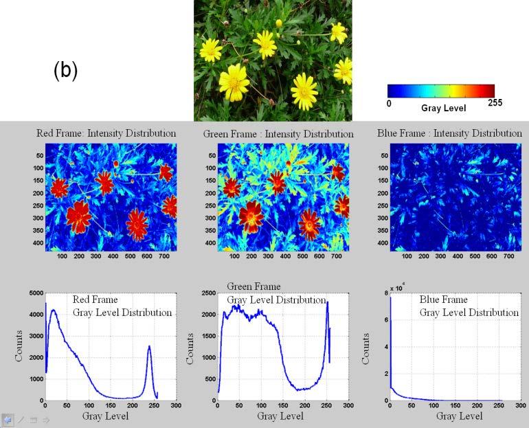
23 Table 1.1 lists the simulated color coordinates and luminance for each primary. From Table 1.1, the color gamut of conventional RGB LCDs is ~76% NTSC. With five primaries, the color gamut increases to 96% NTSC with the same CCFL backlight as Figure 1.5 shows. Moreover, the white luminance is increased by 21% for the five-primary LCD. The increase of white luminance is mainly contributed by the additional yellow and cyan colors. Because we employ more saturated CFs and our RGB pixel numbers are just 60% as compared to a conventional RGB display, we would expect a reduction of RGB luminance for the five-primary display. When the five-primary LCD displays a single primary color, say R, G, or B, the luminance would be lower than that of the three-primary one. However, in real situation, an object that reflects single color or narrow spectral bandwidth (i.e., pure color) will have a very low luminosity. It means the images rarely just show RGB primaries at the highest gray level. In fact, in a RGB-primary display the green luminance should be relatively high because of the need to produce bright yellow and standard white after combining with R and B. While in our five-primary LCD, we could afford to have a more saturated green primary to trade for a wider color gamut because we already have yellow primary. To validate these assumptions, we chose some colorful and representative photos for image analysis. Figure 1.6 shows three photos of the pixel color with respect to gray level distribution. We found in most cases the RGB sub-pixels are usually in the middle range between the maximum (255) and minimum (0) gray levels. The situation of high gray levels usually just happens when displaying yellow objects, e.g., the flowers shown in Figure 1.6(b), or the bright white, e.g., the sky shown in Figure 1.6(c). We realize that all the primaries need to be at the highest gray level while displaying higher luminosity of yellow or white. It means the luminance 10
24 for RGB can be lowered if we have other sources to show yellow and white. Our five-primary design overcomes this problem well because it provides a higher yellow and white brightness than the conventional RGB LCDs due to the extra yellow and cyan. Although the luminance of our RGB colors is lower, it is still high enough to show and reproduce most colored images. When displaying the RGB color contents of an image, we can also adjust the gamma curve to get a better contrast ratio and brightness. According to the metamerism theory [1], there are unlimited choices of weighting ratios for five primaries to reproduce a particular mixed color. In the optimization process, we could choose a higher weighting ratio for Y, G, and C to reproduce a particular color since these three colors have a higher brightness. Therefore, after optimization of color conversion and gamut mapping from three-primary color space into five-primary signals, the decreased RGB brightness would not be a big issue in our five-primary LCDs. On the contrary, we find that five-primary LCDs exhibiting a higher brightness than RGB LCDs when displaying full color images. 11
25 12
 A fruit basket, (b) Lotus in a pond, and (c) a pasture and sky. 1.")
26 Figure 1.6 Image analysis for gray level distributions. (a) A fruit basket, (b) Lotus in a pond, and (c) a pasture and sky. 1.3 Five-Primary LCDs and Comparison Because most input image signals are in three-component format, such as RGB and YCbCr [21], a color conversion algorithm is needed in order to convert the three-primary input into five-primary signals. To do so, we applied the same algorithm developed for multi-primary projection TVs to LCD TVs [22]. Figure 1.7 shows some pictures taken from the 32 five-primary LCD TV prototype. The images of the five-primary LCD TV (left) look much more vivid and brighter than the traditional RGB LCD TV (right). The extra yellow and cyan primaries not only widen color gamut but also 13

27 provide very good color reproduction. The measured data are shown in Figure 1.8 and Table 1.2. The color gamut is increased by 26% and the brightness of white point is also increased by 26%. The agreement between simulated and measured color gamut is within 5%. The possible errors might originate from the spectrum deviation in the mass production of color filters and CCFL. Figure 1.7 Photos from a 32 MVA LCD TV prototype. Left column: five-primary (RGBYC); right column: conventional RGB primaries. Backlight: CCFL in both systems. 14

28 Figure 1.8 Measured data for the RGB and RGBYC MVA LCD TVs. Table 1.2 Measured data for RGB and RGBYC displays. 15
29 As a promising solution for wide color gamut displays, we also compare the performance of our five-primary display with other competing approaches such as RGB-primary using wide gamut CCFL (WG CCFL) (Figure 1.4) and RGB LEDs. Results are summarized in Table 1.3. In our simulations using WG CCFL and RGB LED backlight in the RGB-primary system, the color gamut achieves ~90.23% and 120%, respectively. However, these three-primary based technologies still cannot reproduce good yellow and cyan colors like our five-primary LCD. Table 1.3 Performance comparison of wide-gamut CCFL, RGB LEDs and our five-primary LCDs. We also simulated our five-primary MVA LCD using WG CCFL backlight; its emission spectrum is shown in Figure 1.4. Here, we assume the conventional CCFL and WG CCFL have the same luminosity. From our simulation results shown in Figure 1.9 and Table 1.4, we find that the color gamut reaches ~114.07% NTSC and, moreover, the brightness of white point increases ~7%. Although the yellow brightness is reduced by ~20%, other four primaries experience brightness increase. The better spectrum match between our five-primary CFs and WG CCFL is responsible for the significant increase in brightness. We believe that this could be the highest NTSC ratio ever achieved with such a high efficiency by using a WG CCFL backlight. 16

30 Figure 1.9 Simulated color gamut of RGBYC-primary with conventional CCFL (dashed lines) and RGBYC with WG CCFL (solid lines) in a MVA LCD. Table 1.4 Simulation results on display brightness and color coordinates of our 5-primary MVA LCD using conventional CCFL and WG CCFL. 17
31 1.4 Summary We have successfully developed and demonstrated a five-primary LCD TV prototype. Using the same CCFL backlight and pixel layout and dimension, the color gamut of our fiveprimary display is more than 90% NTSC without sacrificing brightness. This technology is promising for wide color gamut displays. Moreover, ~26% increase in white luminance give us a flexibility to reduce the light source density and power. Low power consumption is highly desirable from energy saving viewpoint. If a WG CCFL is employed, the color gamut of our five-primary MVA LCD is over 114%. 18

32 CHAPTER 2: FIELD SEQUENTIAL COLOR DISPLAY 2.1 Introduction Low power consumption is a critical requirement for all liquid crystal displays, especially for portable electronic devices and large screen TVs. As Figure 2.1 shows, two most lossy components in a LCD system are polarizer and color filters. The polarizer transmits ~45% of the incident backlight, while each color filter only transmits ~30% of the incoming white light. Therefore, the overall transmittance is usually ~5% in a conventional LCD. To overcome the light loss from polarizer, backlight recycling using a reflective polarizer, such as 3M s Dual Brightness Enhancement Film (DBEF) has been widely implemented [23] [24]. Figure 2.1 Optical transmittance of each component in a LCD. 19
![To avoid the dramatic absorption loss from color filters, field-sequential-color (FSC) using red (R), green (G) and blue (B) LEDs has been proposed [25] [26] [27].](/docs-images/71/66148940/images/33-0.jpg "In a FSC LCD, each primary color appears sequentially.")
33 To avoid the dramatic absorption loss from color filters, field-sequential-color (FSC) using red (R), green (G) and blue (B) LEDs has been proposed [25] [26] [27]. In a FSC LCD, each primary color appears sequentially. If the field s frequency is fast enough, the observer s eyes could integrate the sequential fields and perceive the original colored images as Figure 2.2 shows. By using the RGB LEDs backlight in FSC LCDs, we can remove the color filters in a conventional LCD. Therefore, a FSC LCD offers two important advantages over the color filtersbased LCDs: 1) its optical efficiency is improved by ~3X, and 2) the device resolution density is improved by 3X. Figure 2.2 Working principle of the field-sequential-color display. 2.2 Color Breakup In FSC LCDs, the frame rate would be tripled as compared to the conventional LCDs. Therefore, the response time of the LC materials should be at least 3X faster for the FSC LCDs. However, 3X faster of the response time is not enough for FSC LCDs in reality. A biggest challenge for FSC LCDs is the need of fast LC response time in order to suppress the color breakup (CBU) [28] [29] [30] [31] [32]. CBU is the most disturbing defect that degrades the image quality in FSC displays. It can 20

. Figure 2.3 The reason of color breakup.")
34 be observed in stationary or moving images. When our eyes trace a moving object, each sequential color (i.e., R, G, and B) image would project on our retina at different positions as Figure 2.3 shows. Therefore, when there is a relative speed between the images and observers eyes, the observer will see the color splitting patterns or rainbow effect at the boundary between two different colors (Figure 2.4). Figure 2.3 The reason of color breakup. Figure 2.4 Rainbow effect caused by color breakup. 21
35 In order to reduce CBU, we can increase the field frequency to 540 Hz or even up to 1000 Hz [33]. This approach has been widely used in FSC projectors. However, for direct-view LCDs, higher field frequency would require new LC materials with very fast response time (i.e., less than 1ms). Several other methods have also been proposed instead of using new LC materials. Such as inserting another color or black fields [34] [35], motion compensation technique [36], four color fields arrangement [37], and Stencil-FSC method [38]. However, most of these methods still require fast LC response time. Some methods even sacrifice the display brightness and some are restricted by the uncertainty of observers motion. In Chapter 1, we already introduce the principles of five-primary color (R, G, B, yellow (Y), and cyan (C)) LCD which has been shown to exhibit a very good color and brightness [17] [18] [39]. Because of the better color reproduction and optical efficiency, we extend the fiveprimary approach to FSC LCD. We propose a practical way to reduce CBU by using fiveprimary-color technique for direct-view FSC LCD without enhancing the frame rate. Meanwhile, our design not only widens the color gamut but also increases the white brightness, as compared to the three-primary LCD. 2.3 Multi-Primary FSC LCDs The two-dimension time and location diagram is usually used to evaluate CBU (Figure 2.5). By integrating images of consecutive frames along the trace of saccadic eye motion, we can evaluate the color and brightness variations of rainbow-like CBU patterns. From the simulated CBU (Figure 2.6), it shows that the three-primary FSC displays with sub-frame frequency of
36 Hz (i.e., frame rate of 180 Hz) have the CBU width of N pixels. N is determined by the relative speed between the images and observers eyes. Figure 2.6(b) and Figure 2.6(d) show the CBU width for higher and lower frame rates, respectively. We observe that the higher frame rate causes a less noticeable CBU. There is no doubt that increasing the frame rate is an effective way to suppress CBU. However, the requirement for fast LC response time makes this method a challenge. According to the two-dimension time and location diagram shown in Figure 2.5(b), the CBU width for five-primary is 5/3 times more than the three-primary under the same frame rate. Therefore, it is naturally expected that five-primary could suffer from larger CBU as compared to three-primary displays. Some psychophysical experiments about the comparison of CBU visibility between three-primary and five-primary displays have been reported [40]. Surprisingly, the results indicate that, most of the time, CBU for five-primary is less visible than threeprimary. However, thus far there is no further study and systematic analysis for this result. In our simulations based on five-primary, we develop a method to compress CBU by optimizing the color sequence and weighting ratios. 23


37 Figure 2.5 Two-dimension time and location diagram. The upper parts of each diagram represent the moving white objects with width of W pixels. The lower parts are simplified CBU patterns without considering the brightness variation. The slant dashed arrows show the eyes tracking along the movement of object. Figure 2.6 Simulated CBU for three-primary display. (a) White object, (b) Frame rate = 540Hz, (c) Frame rate = 180Hz, (d) Frame rate = 60Hz. 24
38 When a three-primary LCD displays a specific color, there is a unique color ratio corresponding to this color. However, there are numerous possibilities for five-primary. Here, we adopt the commercialized LEDs from Nichia in our simulations. The spectra and luminance intensity are shown in Figure 2.7. From Table 2.1, we find that there are many choices for the five-primary to reproduce the same white color coordinate of standard illuminant D65 (i.e., x = , y = ). In order to choose the best solution among these infinite combinations, we take some basic rules and requirements into considerations. First, we abide to the MacAdam limits [1] which set the theoretical maximum relative reflection and brightness between a specific color and white under D65 illumination. From Figure 2.8, this theorem tells us a reasonable relationship of brightness between each primary should be Y>G, G>R, G>B, G>C, and C>B. Second, we consider the capability of LED brightness of different colors. In the real design of LED backlight, we tend to use the same numbers of LEDs for each primary. We also prefer each LED to work at its maximum luminance, so that we can minimize the number of LEDs. For example, if we choose a ratio of R:G:B to be 10:37:5, it is an acceptable ratio based on the brightness ratio of 10:37.7:9.3 shown in Figure 2.7. However, the ratio of 10:37:12 would not be a good choice because we need more blue LEDs to fulfill the design. Third, we would like to optimize the brightness. Table 2.1 also shows that different ratio would lead to a different brightness and we prefer the ratios with higher brightness. After considering the abovementioned three criteria, we obtain a set of ratios for R:G:B:Y:C to be 12.36:18.90:4.04:48.33:

 Table 2.")
39 Figure 2.7 LED spectra and luminance intensities. (Ref. Nichia Co.) Table 2.1 Color ratios for standard illuminant D65 26
40 Figure 2.8 MacAdam Limit boundaries for the CIE 1931 color space chromaticity diagram. Based on the preliminary color ratios, we simulate the CBU with different color order as Figure 2.9 shows. The left side shows the color order and the right side is the corresponding CBU patterns. In comparison to the CBU of three-primary in Figure 2.9(a), the five-primary has a broader CBU as we expected from time and location diagram (Figure 2.5(b)). However, we can find some better color orders that cause a weaker perceived CBU. For example, Figure 2.9(e) and Figure 2.9(f) exhibit a smaller CBU than those from Figure 2.9(b) to Figure 2.9(d). It is because the high brightness colors, such as yellow and cyan which are in the middle order, tend to merge with the white color of the object. Similarly, the lower brightness colors of red and blue tend to merge with the black background. Due to the lower color contrast and luminance contrast, we perceive that the CBU is compressed. 27
 to Figure 2.")
41 Figure 2.9 Simulated CBU with different color appearing sequence. Although we can continue to optimize the color sequence of RCYGB or RCYBG, we still observe the CBU in five-primary FSC display. To further reduce CBU, we propose to boost the ratio of yellow and cyan brightness; meanwhile, to reduce the red, green, and blue ratios. From Figure 2.10(b) to Figure 2.10(e), the CBU is gradually suppressed when the ratio of red, blue, and green is decreased. The CBU reduction is more pronounced if we could get rid of green completely while reproducing white color. Because of the weaker red and blue colors, these colors are almost merged to the black background. Our eyes also tend to trace the brighter color 28
), we effectively compress the CBU by adjusting the color order and weighting ratios.")
42 fields, such as yellow and cyan, thus, we feel these two colors are merged to the white object. Here, we rearrange the sequence of green to be the last in order to get the least CBU (Figure 2.10(e)). In comparison to the CBU of three-primary (Figure 2.10(a)), we effectively compress the CBU by adjusting the color order and weighting ratios. When we want to realize the lower brightness ratio of R, B, or G, we use the liquid crystal cell to modulate the brightness instead of dimming or turning off the backlight. Therefore, the backlight emits each primary sequentially as the normal FSC backlight. There will be no need to change the electronic control of our five-primary backlight system. Figure 2.10 Simulated CBU with different color weighting ratios. 29
43 Table 2.2 shows some choices of color ratios leading to a fairly small CBU for fiveprimary in representing white color. We would choose the most appropriate ratio after considering the least color shift ( uv) at different viewing angle [10] [17], highest brightness, and least CBU. Usually, the solution for the least color shift might not be the same as that for the highest brightness or least CBU, and we need to compromise between these factors. If the CBU is acceptable, we could choose the ratio with the highest brightness. When showing the lower gray level of white (i.e. lower brightness), we could choose the ratio with the least color shift but not necessarily with the highest brightness. Table 2.2 Color ratios and color shift in IPS mode LCDs Figure 2.11 shows the simulated CBU for yellow and cyan objects. It is easy to realize that a five-primary LCD has no CBU when displaying these two color tones. Unlike a threeprimary LCD which generates yellow by mixing red and green, or cyan by mixing green and blue, the five-primary LCD can just use yellow or cyan LEDs to display these two colors. Ideally, there would be no CBU. 30

44 Figure 2.11 Simulated CBU of yellow and cyan objects. Figure 2.12 shows another two arbitrary colors represented by three-primary and fiveprimary LCDs. Based on the similar method of showing white color object, we boost the ratio of yellow and cyan to get compressed CBU in five-primary. Under proper color sequence and weighting ratios, the CBU of a five-primary display is not always larger than that of threeprimary. On the contrary, after optimization the five-primary LCD could exhibit a smaller CBU than the conventional three-primary. 31

45 Figure 2.12 Simulated CBU of two arbitrary colors. The bottom figures show compressed CBU after adjusting the color weighting ratios. Figure 2.13 shows the color coordinates of LEDs and color gamut of our five-primary display. Because of the additional yellow and cyan sources, the color gamut could achieve ~140% NTSC and it provides a very good color reproduction. 32

46 Figure 2.13 Color coordinates and gamut for five-primary LCDs. We also compare the brightness and numbers of LEDs required between three-primary and five-primary FSC LCDs. In Table 2.3, the luminance intensity means the capability or maximum brightness of a single LED. To satisfy the color ratio we want, we estimate the LED number for each color. Brightness in Table 2.3 means the actual brightness of each color when showing the white color. We notice that not all the LEDs emit light at its maximum luminance. When showing the white color (CIE illuminant D65), the three-primary LCDs have the total brightness of (a.u.) during each frame time (i.e., 3/540 Hz). For the five-primary LCDs, the 33

47 total brightness would be (a.u.). However, under the same sub-frame rate (i.e. 540 Hz) as three-primary, the five-primary LCDs take more time (i.e. 5/540 Hz) to complete each frame. Therefore, the brightness that we perceive in five-primary FSC LCDs should be multiplied by a factor of 3/5. After considering the field sequential factor for five-primary, we find the brightness of (a.u.) in reality. Therefore, the brightness for five-primary is 13% higher than threeprimary FSC LCDs. Table 2.3 The required LED numbers for showing white color (CIE illuminant D65). 34
48 2.4 Discussion and Conclusion From our simulations, we can suppress CBU effectively by choosing proper color order and ratios in the five-primary LCDs. However, a major challenge in our design is the relative low brightness of yellow and cyan LEDs (as of today). From Table 2.3, we realize that the LED numbers we need for yellow and cyan are much more than other primaries. Actually, many LED manufacturers already delve into developing high power yellow and cyan LEDs, and they have obtained promising results and progress recently. We believe this issue could be resolved in the near future. Another difficulty we encounter is how to present our simulated CBU correctly in the three-primary displays. In the three-primary displays, we combine red and green to generate yellow, or green and blue to generate cyan. However, in the five-primary display, there are particular yellow and cyan sources that are more saturated and brighter. Therefore, it is impossible to display the same yellow and cyan colors in three-primary display as shown in fiveprimary displays. In addition, as restricted by the limited brightness of green we cannot generate and display very bright yellow and cyan when showing the simulated patterns of CBU in a threeprimary display. The intrinsic difference between three-primary and five-primary displays becomes a problem during our optimization process. It causes an uncertain issue when we compromise between the CBU, color shift, and brightness to get the best ratio of each primary. This problem can be easily resolved once we use the five-primary display in the simulations and psychophysical experiments. We have developed a method to reduce CBU in five-primary FSC displays. With the same sub-frame rate as three-primary, we effectively compress the CBU by adjusting the color 35
49 order and ratios. In our simulations, the color gamut is 140% NTSC which provides a very good color reproduction. The brightness is also increased by 13% in comparison to three-primary displays. We believe that once the CBU is reduced to an acceptable level, FSC LCD would become a strong contender for next-generation display technology. 36
50 CHAPTER 3: BLUE PHASE LIQUID CRYSTAL DISPLAYS 3.1 Blue Phase Liquid Crystal Introduction In Chapters 1 and 2, we propose a five-primary method to reduce the CBU in FSC LCDs. In order to completely eliminate CBU, increasing the frame rate of the sequential color images is still a viable approach. In addition, the higher frame rate helps to reduce motion blur and improve image quality. The higher frame rate (e.g., >480 Hz) would need very fast response time of liquid crystal (e.g., <1 ms). Presently, the gray-to-gray response time of a nematic liquid crystal is about 5 ms which is still inadequate for FSC LCDs. Recently, optically-isotropic liquid crystals, including polymer-stabilized blue phase (PSBP) and polymer-stabilized isotropic phase (PSIP) liquid crystals draw lots of attentions because of their submillisecond response time [41] [42] [43]. Blue-phase liquid crystals (BPLCs) are often observed in a very narrow temperature range (0.5-2K) between chiral nematic and isotropic phases. In Meiboom s model, BPLCs are comprised of double-twist cylinders arranged in a cubic lattice, where the coexistence of such cylinders and disclination lines stabilizes threedimensional periodic structures as shown in Figure
51 Figure 3.1 Double-twist alignment of LC molecules and cubic structure of BPLCs. The temperature range of BPLCs can be expanded significantly by polymerizing a mixture of monomers that are localized at the disclination cores [41]. A polymer-stabilized BPLC with a temperature range wider than 60K including room temperature ( K) has been demonstrated. The wide temperature enables display applications. The symmetric cubic structures in a PS-BPLC appear optically isotropic at zero electric field, but become anisotropic when a strong field is applied to induce birefringence. The microscopic structure of such induced birefringence is still not yet completely understood, but macroscopically it can be treated as Kerr effect in isotropic materials caused by the electric fieldinduced reorientation of polar molecules. The induced birefringence can be described by Kerr effect equation as: 2 n ind = λke, (1.1) 38
52 where λ is the wavelength of incident light, K is Kerr constant which depends on the wavelength, temperature and driving frequency [43, 44], and E is the applied electric fields. Kerr effect shows a fast response time (<1 ms) due to the short coherent length of BPLCs. For display applications, several advantages make BPLCs quite attractive: 1) no need for alignment layer, 2) initially isotropic dark state, and 3) gray-to-gray response time in submillisecond range so that it has potential to be used for color sequential displays, 3D displays, or photonic devices Planar In-Plane-Switching BPLCD For display applications, the BPLCs are usually driven by planar in-plane switching (IPS) electrodes, where the electric fields are substantially in lateral direction [30] [31]. Figure 3.2 shows a traditional planar IPS-based BPLCD. The substantial lateral electric fields would induce birefringence along the direction of electric fields, provided that the employed LC has a positive dielectric anisotropy. The BPLCs could be optically modeled as an isotropic sphere with E=0. Under crossed polarizers, the display shows a good dark state. As E increases, the induced n changes the sphere into an ellipsoid like a uniaxial medium where the optic axis is along the electric field vector. Therefore, the polarized incident light would experience a double refraction and accumulate certain phase retardation. As a result, the light would transmit through the crossed linear polarizers. The transmittance depends on the applied voltage. 39

53 Figure 3.2 Operation principle of a planar IPS BPLCD between crossed polarizers: (a) E=0, and (b) E>0. Planar IPS is a popular and mature technology which is widely used in nematic LCDs, such as iphones and ipads. In an planar IPS BPLC cell, the electric fields have limited penetration depth into the BPLC layer so that the induced birefringence only happens in less than ~3 µm thickness [45]. The cell gap does not affect the optical property when it is larger than 3 µm. Therefore, the electro-optic properties of a planar IPS BPLCD are insensitive to the cell gap. The operating voltage is a critical issue for planar IPS BPLCDs. A BPLC material with a large Kerr constant (K~10 nm/v 2 ) has been recently developed to reduce the driving voltage from over 100 V rms to ~50 V rms. We can also optimize the electrode width and electrode gap to reduce the operation voltage. From the simulated results, smaller electrode width and gap help to reduce driving voltage with tradeoff in transmittance. However, these voltages are still far beyond the acceptable range of mainstream amorphous-silicon thin film transistors (TFTs), and higher driving voltage also dramatically increases power consumption. Another problem of planar IPS structure is that the electric field direction and intensity profile are not uniform. Therefore, some dead zones exist with very weak or vertical electric fields above the electrodes. 40
54 These dead zones do not contribute to light transmittance, resulting in a reduced optical efficiency (<70%). Moreover, in a planar IPS mode the nonuniform electric fields are particularly strong near electrode edges which could cause lattice deformation, known as electrostriction effect, leading to hysteresis [46] [47]. Therefore, besides developing new BPLC materials with a large Kerr constant, designing new electrodes and driving mechanism play equally important roles for achieving low operation voltage, high transmittance, and hysteresis-free blue-phase LCDs. 3.2 Reducing Voltage for Blue Phase Liquid Crystal Display Planar IPS mode exhibits shortcomings in high operation voltage and relatively large hysteresis. To reduce voltage and hysteresis, some modified IPS structures have been proposed. In order to overcome small penetration depth of the electric fields for IPS structure, a partitioned wall-shaped electrode configuration has been proposed [48]. The parallel wall-shaped electrodes contact top and bottom glass substrate and also work as spacers. In comparison to planar IPS, this structure can generate horizontal electric fields between electrodes and induce uniform birefringence throughout the entire cell gap. From simulation results, the operating voltage is reduced by 1.5X as compared to the planar IPS. However, this structure is difficult to fabricate and has very small aperture ratio which causes low transmittance. In addition, the wallshaped electrodes would block the oblique backlight and sacrifice the brightness at large viewing angle. For the traditional planar IPS structure, the horizontal electric field can be enhanced by reducing the electrode gap. However, the smaller electrode gap causes shallower penetration 41
55 depth which leads to a reduced optical efficiency. A protrusion electrode structure has been proposed for increasing the penetration depth of electric fields [45]. From the simulation results with 2 µm bottom electrode width, 1 µm top electrode width, 2 µm electrode height, and 3 µm electrode gap, the peak transmittance is ~71% (normalized to the transmittance of two parallel polarizers) at 13 V rms. However, the manufacturing of such small protruded IPS electrodes is still a big challenge in industry. Samsung Electronics demonstrated a 15 BPLCD prototype in 2011 by using the protrusion structure of 4-µm electrode width, 4-µm electrode gap, and 2-µm electrode height. From the measured results, the peak operation voltage is reduced from ~60 V rms to ~38 V rms. Semiconductor Energy Lab (SEL) also demonstrated a 6 protruded IPS BPLCD in 2012 with operating voltage ~27 V rms. These results clearly show the improvement on operating voltage by using protrusion electrodes for blue-phase LCDs. Although SEL shows the lowest driving voltage reported so far, it is still too high for LCD applications. In addition, Samsung Electronics indicates that residual birefringence, hysteresis, and voltage holding ratio are still unsolved even with protruded electrodes. The planar IPS electrode with an etched substrate [49] which generates doublepenetrating fringe fields was also proposed. Because BPLCs fill the etched region, it helps to contribute the phase retardation and reduce the driving voltage. With 1 2 µm etching depth, the operating voltage is reduced by 30% as compared to the planar IPS. Further improvement by deeper etching is limited because the lateral electric fields only penetrate ~3 µm. This etched IPS BPLCD also exhibits a wider viewing angle because of the created multi-domain structures in the etched areas. However, this method complicates the manufacturing process and the driving voltage is still too high. 42
56 A corrugated electrode for BPLCD was proposed to reduce operating voltage and enhance the transmittance [50]. The periodic corrugated electrodes on the top and bottom substrates can generate a strong horizontal component of electric field to induce a large birefringence of BPLCs. Moreover, this field is uniformly distributed across the entire pixel area and penetrates deeply into the BPLC medium. The accumulated phase retardation along the beam path is large, resulting in high transmittance and low voltage. From simulations, the driving voltage can be reduced from ~50 V rms for planar IPS to ~9.9 V rms for corrugated structure. The transmittance is also improved (~85.6%) as compared to planar IPS (~65%) because of the uniform electric fields across the pixels and smaller dead zones. This result shows a possibility for TFT addressing and BPLCD applications. Unfortunately, the manufacturing process of the TFT on the corrugated structure is still an issue so far. In addition to lateral electric fields discussed above, another possibility to drive BPLC devices is to use longitudinal field, which is proposed independently by us [51] and by Kim et al [52]. In Ref. [52], the normal incident backlight is split into two oblique angles by a bottom prism sheet. A top prism sheet is used to orient the oblique light back to the normal direction. The oblique light inside the BPLC can accumulate the necessary phase retardation for achieving continuous grayscales under applied vertical field. Because there is no patterned electrode inside the cell, the cell structure is much simpler than the protruded IPS. However, there are several intrinsic problems of this design. First, the split backlight by the bottom prism sheet would cause double images which in turn degrade the resolution and image quality. Second, the top and bottom prism sheets sandwiched between a polarizer and an analyzer would depolarize the incident backlight and decrease the contrast ratio dramatically. Furthermore, the driving voltage 43
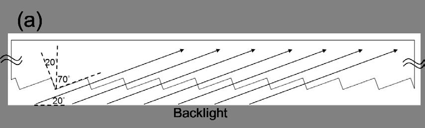
57 is still too high for TFT addressing and the optical efficiency in this design is also questionable. 3.3 Vertical Field Switching BPLCD Although abovementioned methods have been proposed to overcome the high voltage problem of BPLCDs, results are still unsatisfactory. Most of the proposed methods do increase the complexity of manufacturing process. Hysteresis is another important issue. Some of the designs are helpful for reducing hysteresis, but none is actually free from hysteresis. Here, we propose vertical field switching (VFS) for a BPLCD with obliquely incident light to achieve low voltage, high transmittance, and hysteresis-free operation [51] [53] Device Structure Figure 3.3 depicts our proposed VFS BPLC device structure. The electric field inside the cell is in the longitudinal direction, and only the incident light at an oblique angle (0<θ<90 ) can experience the phase retardation effect. For a given BPLC layer thickness, a larger incident angle results in a larger phase retardation, which is helpful for lowering the operation voltage. Hence, we couple the backlight to a large output angle (e.g., θ~70 ) and keep it reasonably well collimated. The reason of a well-collimated light is to achieve better viewing symmetry. If the incident light is divergent, the portion with a smaller angle would accumulate less phase retardation and has lower gray levels, while the larger angle part would accumulate more phase retardation and result in higher gray levels. In this case, the divergent backlight would cause asymmetric brightness distribution when viewed from right side or left side of the panel after the light exits to the viewer s side. As a result, it will be difficult to obtain uniform brightness. The 44
![well-collimated backlight is already adopted in some high brightness LCDs and 3D displays [54] [55]. In our design, the polarizer and analyzer are set at 45 and -45 azimuthal angles.](/docs-images/71/66148940/images/58-0.jpg "The prism films (i.e., coupling films and turning film) are set at 90 as Figure 3.3 shows. We used the ray tracing software (i.e. LightTools) to simulate this structure.")
 and the maximum intensity is at 70. Figure 3.3 Device structure of the proposed VFS-BPLCD. Figure 3.4(a) shows the structure of a bottom coupling film laminated on the bottom polarizer.")
58 well-collimated backlight is already adopted in some high brightness LCDs and 3D displays [54] [55]. In our design, the polarizer and analyzer are set at 45 and -45 azimuthal angles. The prism films (i.e., coupling films and turning film) are set at 90 as Figure 3.3 shows. We used the ray tracing software (i.e. LightTools) to simulate this structure. Referring to the commercialized prism film (e.g., 3M s brightness enhancement film), the refractive index of our prism films is ~1.59 and the thickness is ~150 µm. The backlight has a reasonable Gaussian distribution (FWHM ~30 ) and the maximum intensity is at 70. Figure 3.3 Device structure of the proposed VFS-BPLCD. Figure 3.4(a) shows the structure of a bottom coupling film laminated on the bottom polarizer. It can substantially couple the oblique incident light to the bottom substrate and the 45
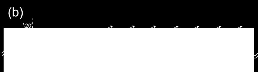
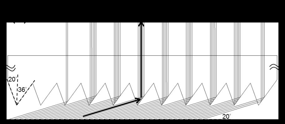
59 BPLC layer as well. The prismatic structure not only couples the oblique input light to the cell but also keeps a large incident angle in the BPLC layer. Without the bottom coupling film, the refraction angle in the BPLC layer will be reduced dramatically according to Snell s law. As a result, the phase retardation will be smaller and the operating voltage will be higher. Therefore, how to optimize the prism structure is important to the VFS mode. The prism pitch should be smaller than each pixel size of the LCD; it could range from ~5 μm to ~50 μm. Figure 3.4(b) shows the structure of a top coupling film. Without this top coupling film, the oblique light will be trapped in the cell module because of total internal reflection (TIR). Therefore, the major function of the top coupling film is to couple the oblique light to the air. The prism structures with internal angles of can efficiently couple the light out of the substrate. A pair of top and bottom coupling films plays an important role on keeping a large incident angle in the VFS LCDs. Figure 3.4(c) depicts the structure of the turning film. It can steer the direction of the oblique light to the viewer s position by TIR without any energy loss. The pitch of the turning film is designed to be the same as that of the top coupling film. Therefore, the turning film can be easily laminated or placed on the top coupling film. Because the backlight that we used is well collimated, the turning film with regular prisms is suitable for the narrow-view application. The angle of the turning film should be optimized according to the profiles and angle of the backlight. To realize wide viewing angle, we can use irregular prism, or using the round shaped prisms to spread the light to multiple directions as shown in Figure 3.4(d). The round shaped prisms should provide a wider viewing angle and more uniform image. It should also be more durable than triangular prisms. 46
60 47
.")

61 Figure 3.4 Structures of (a) bottom coupling film, (b) top coupling film, (c) turning film with regular-angle prisms, and (d) turning film with round shaped prisms Experiments and Simulations We performed some experiments to confirm the advantages of our VFS device over the conventional planar IPS structure. Figure 3.5 shows our experimental setup. To simulate the beam path shown in Figure 3.3, we prepared a transparent container filled with Glycerol (n=1.47@ λ=633 nm). The BPLC cell was immersed in Glycerol and it could be rotated freely. Because of matched index between glass and Glycerol, the light can pass through the BPLC without refraction and in a very large angle. 48
![Figure 3.5 Experimental setup for characterizing the VFS cell. We prepared a polymer-stabilized BPLC material from Chisso JC-BP01M [56].](/docs-images/71/66148940/images/62-0.jpg "The LC host has a dielectric anisotropy ε~94 and birefringence n~0.17. The phase transition temperature of the precursor is BP 42.4 C N* during the cooling process and N* 44.")
62 Figure 3.5 Experimental setup for characterizing the VFS cell. We prepared a polymer-stabilized BPLC material from Chisso JC-BP01M [56]. The LC host has a dielectric anisotropy ε~94 and birefringence n~0.17. The phase transition temperature of the precursor is BP 42.4 C N* during the cooling process and N* 44.5 C BP during the heating process, where N* denotes chiral nematic phase. The phase transition temperature between isotropic phase and blue phase was not easy to determine precisely because Bragg reflection occurred at ~350 nm. UV stabilization curing process was performed at 44 C for 30 min. with an intensity of 2 mw/cm 2. After UV curing, the blue-phase temperature range was widened from <0 C to ~70 C. To make a fair comparison, we used the same material for both IPS and VFS cells. The IPS cell has patterned ITO electrodes with 10 µm electrode width and 10 µm electrode gap, and 7.5 µm cell gap. For the VFS cell, both top and bottom glass substrates were coated with thin ITO electrodes; no polyimide layer was used. The cell gap we used was d~5.74 µm. Figure 3.6 depicts the measured voltage-dependent transmittance (VT) curves (at λ=633 nm and T~23 C) of the IPS cell and VFS cell at θ=70. For the IPS cell measured at normal 49
63 incidence, the peak voltage occurs at V p ~50 V rms. For the VFS cell at θ=70, its V p ~16 V rms which is ~3.2X lower than that of IPS structure. To further reduce operating voltage, we could use a larger Kerr constant BPLC or increase the incident angle. Figure 3.6 Measured VT curves and hysteresis of IPS and VFS cells. λ=633 nm. Hysteresis is a common phenomenon for polymer-stabilized liquid crystal devices [46] [47]. For display applications, hysteresis affects the accuracy of grayscale control and should be eliminated. Hysteresis is defined by the voltage difference ( V) at half-maximum transmittance when we scan the voltage forward and backward. From Figure 3.6, the measured V/V p is ~5.8% for the IPS cell. For our new VFS cell with d=5.74 µm and θ= 70, it is free from hysteresis! The reason is that our VFS cell has a weak electric field (E~2.8 V/µm) so that the electrostriction effect does not occur. On the contrary, in an IPS cell the generated electric fields 50
64 are not uniform spatially. The electric fields are much stronger near the pixel edges than those in the electrode gap. The peak electric fields could cause lattice deformation locally which results in hysteresis. To validate this hypothesis, we applied different voltages (up to 40 V rms ) to our VFS cell and measured their hysteresis at θ=70. Figure 3.7 shows the field intensity versus corresponding phase retardation under the specified voltages. The black line represents the ascending curve, while red cycles, blue triangles, and green squares denote the descending curves from 40 V rms, 28 V rms, and 20 V rms, respectively. From Figure 3.7, we find the accumulated phase increases almost linearly and then gradually saturates as the electric field exceeds ~6V/µm. For the V=20 V rms curve (E~3.5 V/µm in our 5.74-µm VFS cell), the forward and backward curves overlap very well and no hysteresis is observed. Therefore, the critical field (E c ) for a hysteresis-free BPLC using Chisso JC-BP01M is ~3.5 V/µm. In our VFS cell, the electric field is uniform, thus it provides a reliable way for determining the critical field for a PS BPLC. On the other hand, for an IPS cell the electric field near electrode edges is often higher than 3.5 V/µm so that it exhibits a noticeable hysteresis. Residual birefringence is another serious problem for IPS BP-LCDs [57]. It causes light leakage at dark state and degrades the contrast ratio. In an IPS cell, the residual birefringence arises in the region with strong field. In a VFS cell, the required field intensity for producing 1π phase retardation is relatively weak. Thus, the resultant residual birefringence is negligible. 51
65 Figure 3.7 Measured phase retardation vs. electric field intensity under different applied voltages. λ=633 nm. We also compared the response time of our VFS cell with IPS cell at 23 C. Figure 3.8(a) shows the gray-to-gray response time of the IPS cell while Figure 3.8(b) shows the measured response time of our new VFS cell. The applied voltage swings from 0 to 16 V rms (@ 100Hz) for the VFS cell, and 0 to ~46 V rms for the IPS cell. We find that IPS cell has a very slow rise time especially in the low gray level transition. Our VFS mode shows much faster rise time and fall time as compared to the IPS cell. Again, this is attributed to the smaller LC reorientation angle and uniform field of the VFS cell. 52
66 Figure 3.8 Measured response time of (a) IPS cell and (b) VFS cell. λ=633 nm. Unlike an IPS cell whose VT curve is insensitive to the cell gap, the peak transmittance voltage of our VFS cell is dependent on the cell gap. Here, two factors have to be considered: induced birefringence and effective cell gap. At a given voltage V, as the cell gap d decreases the 53
67 electric field E gets stronger because E=V/d. According to Kerr effect, the induced birefringence is proportional to E 2. Thus, the induced birefringence is larger as the cell gap decreases. On the other hand, for a given incident angle the beam path in the BPLC cell for accumulating phase retardation decreases as the cell gap decreases. Therefore, there ought to be an optimal cell gap for achieving certain phase retardation. If the cell gap is too thin, although the induced birefringence is large, the optical beam path is decreased so that the accumulated phase may not be adequate for achieving maximum transmittance. Moreover, the saturation phenomenon in the high field region should be also considered. In a real situation, the induced birefringence will gradually saturate as the electric field increases. Therefore, the driving voltage could not decrease indefinitely when we use an ultra-thin cell gap, as described by the extended Kerr effect equation [58]. In the extended Kerr effect model, the induced birefringence is expressed as follows: 2 E n = n sat 1 exp, (1.2) Es where n sat stands for the saturated induced birefringence and E s represents the saturation field. From the measured results in Figure 3.6, our PS-BPLC material has K~7.5 nm/v 2 at λ=633 nm in the low field region, with n sat ~0.17 and E s ~6.0 V/µm. The Kerr constant extracted from VFS cell is ~70% smaller than that from IPS cell. A possible explanation is as follows. In an IPS cell, the electric field varies largely from electrode edges to the center of electrode gap. Therefore, the extracted Kerr constant thru curve fitting has a larger uncertainty. Figure 3.9 shows the simulated VT curves for d=5μm, 2μm, and 1μm at λ=550 nm. For display applications, we often optimize the device design at λ=550 nm. To obtain the Kerr 54
68 constant at this wavelength, we use the value measured at λ=633 nm and then extrapolate it following the dispersion relation [59]. For the 1-µm BPLC cell, the induced birefringence gradually saturates so that the maximum phase retardation reaches ~1π at a fairly high voltage. As compared to the IPS structure whose VT curve is insensitive to the cell gap, the electro-optic effects of VFS are dependent on the cell gap. We can optimize the cell gap according to the material properties and incident angle to obtain a proper operation voltage. If we would compromise for a lower transmittance, we could use a thinner cell gap to trade for a lower operating voltage. For example, from Figure 3.9 the 1-µm VFS cell has an operating voltage of 6 V rms at 70% transmittance, which is the typical transmittance of an IPS cell. If we want to boost the transmittance to 90% for the 1-µm VFS cell, then we can increase the operating voltage to 7.7 V rms. A caution should be taken that if we use a thinner cell gap to reduce driving voltage, the electric filed might exceed the critical field (E c ) for causing hysteresis. The critical voltage for the 5μm, 2μm, and 1μm cells is 17.5 V rms, 7.0 V rms, and 3.5 V rms, respectively. 55
69 Figure 3.9 Simulated VT curves under different cell gap (d= 1μm, 2μm, and 5μm) for the VFS cell. Incident angle=70 o and λ=550nm. Based on the extended Kerr effect, we simulated the cell gap versus the driving voltage at λ=550 nm as shown in Figure As the cell gap decreases, the driving voltage decreases and then reaches a minimum. For the case of θ=70 and d~1.5 μm, the minimum peak voltage occurs at V p ~9 V rms. As stated above, we can optimize cell gap according to the material properties and incident angle to obtain the minimum voltage. For the BPLC layer under a longitudinal field, the induced birefringence n is along the electric field and behaves as a C-plate [60]. The phase retardation Г equals 1π for the first maximum transmittance and can be expressed as: 56
70 57 ( ) ( ) π θ θ λ π = = Γ sin 1 sin 1 2 o g e g o n n n n d n, (1.3) where d is the cell gap, n g is the refractive index of Glycerol (Figure 3.5), θ 0 is the incident angle, and n o and n e are the ordinary and extraordinary refractive indices of the BPLC. We also assume the following equations hold for n o and n e [20]: n n n n n n i e i o + = = 3 2 ; 3 1, (1.4) where n i is the isotropic refractive index of BPLC in the voltage-off state, and Δn is the induced birefringence under an external electric field. After combining equations (1.2), (1.3), and (1.4), we derive (by neglecting algebraic derivation) following analytical solution of cell gap d for the minimum operating voltage: ( ) 1 5 sin sin = s g g i i n n n n n d θ θ λ, (1.5)
71 Figure 3.10 Simulated operating voltage vs. cell gap at different incident angles of VFS cells. λ=550 nm and Kerr constant is assumed to be K~7.5 nm/v 2. The operating voltage is roughly proportional to the inverse square root of Kerr constant under low fields [31] [58]. From Kerr effect equation, we can get Kerr constant K = Δn s / (λe 2 S ). Therefore, BPLC materials with high Δn s and low E S are crucial for enhancing Kerr constant, which subsequently corresponds to the lower operation voltage. Figure 3.11 shows the operating voltage versus cell gap with different Kerr constants. The incident angle is 70 and the wavelength is λ=550 nm. The cyan squares, blue triangles, and red circles denote the same Kerr constant but with different n s and E S respectively. When the Kerr constant is doubled (i.e. K= 15 nm/v 2 at λ=633 nm), the operating voltage is reduced from ~10.9 V rms to ~7.4 V rms in a 3-µm cell gap. We notice that if we can use a BPLC with high n s in an ultra-thin cell gap (e.g. ~1.1 58
72 µm), the driving voltage could be further reduced to below 5V. To get such a large n s, the host LC should have a fairly high birefringence. However, this kind of liquid crystal usually has UV stability issue and high viscosity which is unfavorable for response time. Another strategy to get large Kerr constant is to reduce E S by using materials with a large dielectric anisotropy which would also inevitably increase the viscosity. Therefore, how to lower the operation voltage while keeping fast response time remains a critical challenge for future BPLC development. Figure 3.11 Simulated operating voltage vs. cell gap with different Kerr constants. The optical efficiency (normalized to two parallel polarizers) of an IPS BPLC cell is generally limited to ~70% due to some dead zones above the electrodes. Our VFS cell could in principle achieve 100% transmittance because of its uniform vertical fields without dead zones. The major optical loss comes from Fresnel reflection of the coupling films and turning films. 59

73 From our simulations, the optical efficiency for the employed films is over 85%. Crosstalk between two adjacent pixels would also affect the transmittance of our VFS BPLC. As shown in Figure 3.12, the width W of crosstalk equals d/cotθ, here d is the cell gap, and θ is the incident angle. Therefore, the transmittance ratio becomes 1-W/p, here p is each pixel width. Let us assume d=3µm, θ=70, and p=180µm, the transmittance would be 95%. We can fabricate TFT structure in the crosstalk region and add black matrix on it. Therefore, VFS should have a comparable or higher optical efficiency than IPS. Figure 3.12 Possible crosstalk in a VFS BPLCD. Achieving wide viewing angle is a major challenge for the VFS mode. Because the backlight s incident angle is fairly large through the polarizer and analyzer, the extinction ratio of polarizer and analyzer degrade dramatically. As a result, the intrinsic contrast ratio is very poor for the case of oblique incident light in VFS BPLCD. We need to design some phase compensation methods and retardation films to improve the intrinsic contrast ratio. Since we adopt the directional backlight with fairly narrow FWHM for VFS BPLCDs, this design is suitable for narrow-view applications. To widen the viewing angle, we can design the irregular prism structure of turning film [53] or a front diffuser [61] to orient and steer backlight to different viewing angles. We can also add a polymer-dispersed liquid crystal (PDLC) [62] [63] 60
74 layer in front of the panel to work as a dynamic diffuser. The scattering degree of the PDLC layer can be controlled by the applied voltage. Therefore, we can realize the tunable viewing angle display which is suitable for both private and public environments. 3.4 Summary The VFS mode offers superior performances to IPS in lower operating voltage, higher transmittance, free from hysteresis, no residual birefringence, and faster response time. Its cell structure is very simple, but it requires sophisticated phase compensation scheme to achieve wide view. On the other hand, IPS requires protrusion electrodes to reduce operation voltage, but its phase compensation scheme for achieving wide view is relatively simple. The VFS mode is particularly attractive for displays and photonic devices that require fast response time. 61
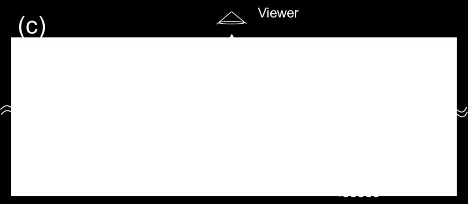
75 CHAPTER 4: WIDE VIEWING ANGLE OF VFS BPLCD From our introductions in the previous chapters, most BPLC devices utilize planar IPS or protruded IPS. Planar IPS has wide view, but its operating voltage is high and hysteresis is fairly large because the lateral field is spatially nonuniform and the peak electric field near electrode edges is high. Protruded electrodes lower the operation voltage, but the tradeoff is increased fabrication complexity. To overcome the fabrication problem, we proposed vertical field switching (VFS) for BPLCDs. With this novel VFS mode, the operating voltage is greatly reduced and hysteresis is completely suppressed. However, how to achieve wide view becomes a challenge. In this chapter, we present several approaches for improving the contrast ratio (CR) and viewing angle of VFS BPLCDs. We also analyze the pros and cons of each method. 4.1 Light Leakage in VFS BPLCD Figure 4.1 depicts the angular distribution of the directional backlight [54] [55] for VFS BPLCDs. A directional backlight with oblique output (θ~70 ) is adopted. A larger incident angle results in a larger phase retardation which helps to lower the operating voltage. Typically, the directional backlight has a divergence angle (full width at half maximum FWHM) smaller than 20. The more collimated backlight is preferred, but we also need to consider the optical efficiency and brightness uniformity. 62
, there is light leakage at the dark state if the polarizer and analyzer are set at ϕ=45 and -45 as a conventional LCD")
76 Figure 4.1 Directional backlight s angular distribution. The polar coordinate in our device and simulations is defined in Figure 4.2. Because the backlight passes the polarizer and analyzer obliquely (θ~70, ϕ~270 ), there is light leakage at the dark state if the polarizer and analyzer are set at ϕ=45 and -45 as a conventional LCD [64]. To minimize light leakage, we can rotate the absorption axes of polarizer and analyzer along ϕ=71.12 and respectively as shown in Figure 4.3(a), in which the polarizer and the analyzer are crossed at the backlight angle (θ=70, ϕ=270 ) as Figure 4.3(b) shows. θ = 0 θ = 90 ϕ = 90 Light source θ = 90 ϕ = 180 θ = 90 ; ϕ = 270 θ ϕ Liquid crystal cell θ = 90 ϕ = 0 Lightguide Figure 4.2 Polar coordinate of the VFS-BPLCD. 63
77 We used commercial software, LCD Master (Shintech), and Nitto Denko s polarizer and analyzer (SEG1425DU) in our simulations. The BPLC composite is optically isotropic with n i =1.55 at the voltage-off state. As the voltage increases, Kerr effect-induced birefringence gradually increases. At V=16 V rms in which the phase retardation δ=π at 70 incident angle of our VFS cell, the measured n o =1.54 and n e =1.57 at λ=633 nm. The cell gap is 4.74µm. Figure 4.3(c) shows the simulated isocontrast contours of Figure 4.3(b) after the incident oblique backlight is steered to the normal direction by a turning film. Although the polarizer and analyzer are crossed at (θ=70, ϕ=270 ), the intrinsic CR is much lower than that of the crossed polarizers at normal incidence. Because the extinction ratio of the analyzer decreases drastically as the polar angle θ increases, in which the smaller effective absorption coefficient causes light leakage in the dark state. Therefore, how to enhance the intrinsic CR and widen the isocontrast contours becomes an urgent task for VFS BPLCDs. 64
 Figure 4.")
, the polarizer and analyzer at ϕ=71.12 and -71.")
78 (a) Absorption axis of polarizer (b) Absorption axis of polarizer ϕ = ϕ = 0 ϕ = 45 ϕ = 0 Absorption axis of analyzer Absorption axis of analyzer (c) Figure 4.3 Change in the effective angle between the polarizer and the analyzer: (a) normal observation (θ=0 ), (b) oblique observation (θ=70 ); (c) simulated isocontrast contours. 4.2 Film Compensation Principles As plotted in Figure 4.3(c), the polarizer and analyzer at ϕ=71.12 and leads to a fairly poor contrast ratio and narrow viewing angle. We could design retardation films to widen the isocontrast contours. However, the maximum CR (or the intrinsic CR) is not improved. On 65
79 the other hand, we could reduce the azimuthal angle ϕ to enhance the effective absorption coefficient and improve the intrinsic CR. In this case, the polarizer and analyzer are not mutually perpendicular at the viewing angle of θ=70 and ϕ=270. It would be even harder to design the phase compensation films to widen the isocontrast contour for a small ϕ. According to our experience, we should find a balance between high CR and wide isocontrast contour by choosing a proper ϕ between the polarizer and the analyzer. Figure 4.4(a) shows our first proposed optical configuration for VFS BPLCD. The absorption axes of polarizer and analyzer are along ϕ =45 and -45 respectively. Because the effective angles between polarizer and analyzer become and rather than mutually perpendicular at oblique incident angle (θ=70, ϕ=270 ), the noticeable light leakage degrades the CR dramatically. We add two identical biaxial films set at ϕ=38.5 and to reduce the light leakage. The N z factor, which is defined as (n x -n z )/(n x -n y ), is 0.54 for both biaxial films, and d(n x -n y ) =256 nm, here d is the biaxial film thickness. Figure 4.4(b) shows the compensation process for the dark state on the Poincaré sphere. At normal incidence, i.e., θ=0, the polarization state after polarizer P 0 is the same as the absorption axis of analyzer A 0. However, the effective angle between the polarizer and the analyzer changes as the incident backlight tilts away from normal (e.g., θ=70, ϕ=270 ). Therefore, the transmittance state P 1 deviates from analyzer A 1 and the light leakage happens. We add two biaxial films to compensate the separation of P 1 from A 1. Biaxial film 1 shifts the polarization state from P 1 to P 0, and subsequently biaxial film 2 moves the polarization state from P 0 to A 1. As a result, light leakage is suppressed substantially. Figure 4.4(c) shows the simulated CR and isocontrast contours optimized at incident angle (θ=70, ϕ=270 ) for λ=550 66
80 nm. From Figure 4.4(c), CR>1000:1 covers ~10 viewing cone which is sufficient for the employed directional backlight (FWHM <20 ) in our VFS BPLCD. In order to widen the viewing angle, a front diffuser [61] [65] or a curve shaped turning film [53] can be applied to spread the directional backlight to the observer for achieving wide view. Figure 4.4(d) shows the simulated isocontrast contours and optical configuration which is optimized for a smaller incident polar angle θ=60, ϕ=270. The polarizer and analyzer are still set at ϕ=45 and -45. Two identical biaxial films (N z =0.63, d(n x -n y ) =260 nm) are set at ϕ=42 and -42. Under a smaller polar angle θ, Figure 4.4(d) shows wider isocontrast contours as compared to Figure 4.4(c). However, a smaller incident angle θ corresponds to a lower induced birefringence of a VFS BPLC which leads to a higher operating voltage. Recently, Merck reported a high Kerr-constant BPLC material [66]. If we use this material, we can choose a smaller incident angle to obtain 1π phase retardation. A smaller incident angle helps to enlarge the isocontrast contours. 67
 Polarizer 45 Coupling film (b) A 1 S 2 A 0 P 0 P1 (c) S 3 S 1 (d) cell Coupling/turning films Analyzer -45 Biaxial film 2 (Nz 0.")
 device configuration, (b) compensation principle on Poincare sphere, and simulated isocontrast")
81 (a) cell Coupling/turning films Analyzer -45 Biaxial film 2 (Nz 0.54, dδn 256, ) Biaxial film 1 (Nz 0.54, dδn 256, 38.5 ) Polarizer 45 Coupling film (b) A 1 S 2 A 0 P 0 P1 (c) S 3 S 1 (d) cell Coupling/turning films Analyzer -45 Biaxial film 2 (Nz 0.63, dδn 260, -42 ) Biaxial film 1 (Nz 0.63, dδn 260, 42 ) Polarizer 45 Coupling film Figure 4.4 Biaxial film-compensated VFS BPLCD: (a) device configuration, (b) compensation principle on Poincare sphere, and simulated isocontrast contours at incident angle θ=70 (c) and θ=60 (d). λ=550 nm. 68
82 Let us return to the backlight angle (θ=70, ϕ=270 ) but varying the polarizer/analyzer angle. Figure 4.5(a) shows the isocontrast contours at a smaller angle (ϕ=40 and -40 ) between the polarizer and the analyzer. Two biaxial films (N z =0.506, d(n x -n y )=259 nm) are set at ϕ=36 and -36. Figure 4.5(b) shows the isocontrast contours when the polarizer and the analyzer are further reduced to ϕ=30 and -30. The incident angle of backlight is still at (θ=70, ϕ=270 ). Two biaxial films (N z =0.44, d(n x -n y )=264 nm) are set at ϕ=31 and -31. Comparing Figure 4.4(c), Figure 4.5(a), and Figure 4.5(b), we find the contour size for CR=1000:1 is similar but the contour shape changes as the absorption angle ϕ between the polarizer and analyzer varies. For practical applications, we should also consider the output profile of the directional backlight in order to choose an appropriate ϕ and the matched contour shape. Figure 4.6 shows the isocontrast contours optimized for a smaller incident polar angle (θ=60, ϕ=270 ). The polarizer and the analyzer are set at ϕ=30 and -30. Two identical biaxial films (N z =0.4775, d(n x -n y )=264.5nm) are set at ϕ=32.5 and From Figure 4.4(d) and Figure 4.6, a smaller incident polar angle could result in larger contours. 69
83 (a) cell Coupling/turning films Analyzer -40 Biaxial film 2 (Nz 0.506, dδn 259, -36 ) Biaxial film 1 (Nz 0.506, dδn 259, 36 ) Polarizer 40 Coupling film (b) cell Coupling/turning films Analyzer -30 Biaxial film 2 (Nz 0.44, dδn 264, -31 ) Biaxial film 1 (Nz 0.44, dδn 264, 31 ) Polarizer 30 Coupling film Figure 4.5 Simulated isocontrast contours of biaxial film-compensated VFS BPLCD: (a) ϕ=40 and -40 and (b) ϕ=30 and
84 Figure 4.6 Isocontrast contours and film configurations of a VFS BPLCD with incident angle θ=60. Figure 4.7(a) shows another compensation method by adding four biaxial films. The polarizer and the analyzer are set at ϕ=30 and -30. Two identical biaxial films 1 and 4 (N z =0.851, d(n x -n y )=281nm) are set at ϕ=25.75 and Identical biaxial films 2 and 3 (N z =0.3984, d(n x -n y )=272nm) are set at ϕ=29.72 and The compensation process is shown on the Poincaré sphere in Figure 4.7(b). As compared with previous examples, the additional two biaxial films are designed to compensate the varied effective angle between the polarizer and the analyzer due to different azimuthal angle ϕ. P 2 denotes the polarization state at θ=70, ϕ=300. P 2 deviates from P 1 which represents the transmittance state at θ=70, ϕ=270. The biaxial film 1 can compensate the effect of varied ϕ and shift the polarization state from P 2 to P 1. The biaxial films 2 and 3 shift the polarization state from P 1 to A 1. Finally, the biaxial film 4 shifts the polarization state to absorption axis of the analyzer A 2. Figure 4.7(c) shows the CR contours. Because of two additional biaxial films to compensate the effect of varied azimuthal angle ϕ, the CR contours exhibit a more circular shape which is similar to the output profile of the direction backlight. 71

 film")

85 Figure 4.7 Optical configuration of the proposed VFS BPLCD: (a) film configuration, (b) compensation principle, and (c) isocontrast contours. 72
86 Figure 4.8(a) shows another example of four biaxial films. The polarizer and analyzer are set at ϕ=45 and -45. The biaxial films 1 and 4 (N z =0.575, d(n x -n y )=256 nm) are set at ϕ=40 and -40. The biaxial films 2 and 3 (N z =0.5, d(n x -n y )=137 nm) are set at ϕ=90 and ϕ=0, respectively. From the Poincaré sphere in Figure 4.8(b), biaxial film 1 shifts the polarization state from P 1 to P 0. Biaxial film 2 shifts the linear polarization state P 0 to circular polarization C 1, and then biaxial film 3 changes the circular polarization C 1 back to linear P 0. Finally the biaxial film 4 rotates the transmission state P 0 to align with the absorption axis of analyzer A 1. Here, P 0 and A 0 are for the normal incident θ=0. P 1 and A 1 deviate from P 0 and A 0 due to the oblique incidence (θ=70, ϕ=270 ) of the directional backlight. Because the circularly polarized light C 1 is independent of the azimuthal angle ϕ in the BPLC material, it helps to improve the brightness state of the VFS BPLCD. Actually, we also tried to use one biaxial film to shift the polarization state from P 1 to C 1 directly and another biaxial film to shift the polarization state from C 1 to A 1. However, this simpler configuration is very sensitive to the polar angle θ and our results are not promising. Figure 4.8(c) shows the isocontrast contours when the directional backlight is at (θ=70, ϕ=270 ). Figure 4.8(d) shows the isocontrast contours optimized for the incident angle (θ=60, ϕ=270 ) of the directional backlight. The polarizer and the analyzer are set along ϕ=45 and -45. The biaxial films 1 and 4 (N z =0.63 and d(n x -n y )=260nm) are set at ϕ=42 and -42. The biaxial films 2 and 3 (N z =0.5 and d(n x -n y )=137nm) are set at ϕ=90 and 0, respectively. Figure 4.8(d) exhibits wider isocontrast contours than Figure 4.8(c) because of the smaller incident angle. 73
 Biaxial film 1 (Nz 0.")
 Biaxial film 3 (Nz 0.5, dδn 137, 0 ) Biaxial film 2 (Nz 0.63, dδn 260, 42 ) Polarizer 45 Coupling film Figure 4.")
87 (a) cell Coupling/turning films Analyzer -45 Biaxial film 4 (Nz 0.575, dδn 256, -40 ) Biaxial film 3 (Nz 0.5, dδn 137, 0 ) Biaxial film 2 (Nz 0.5, dδn 137, 90 ) Biaxial film 1 (Nz 0.575, dδn 256, 40 ) Polarizer 45 Coupling film (b) A 1 S 2 A 0 P 0 P1 (c) S 3 C 1 S 1 (d) cell Coupling/turning films Analyzer -45 Biaxial film 4 (Nz 0.63, dδn 260, -42 ) Biaxial film 3 (Nz 0.5, dδn 137, 0 ) Biaxial film 2 (Nz 0.5, dδn 137, 90 ) Biaxial film 1 (Nz 0.63, dδn 260, 42 ) Polarizer 45 Coupling film Figure 4.8 Optical configuration of a VFS BPLCD with 4 biaxial films: (a) film configuration, (b) compensation principle, and simulated isocontrast contours at θ=70 (c) and θ=60 (d). 74
88 In all the above examples, the backlight passes the analyzer obliquely. If the coupling film and turning film are laminated between the analyzer and the BPLC cell, the light would pass the analyzer at normal angle and the analyzer would exhibit a good extinction ratio. Moreover, better image quality can be obtained if the coupling film and turning film are closer to the image plane (i.e., pixels of the LCD panel). Similarly, if we can place the polarizer outside the bottom coupling film [Figure 4.9(a)], the directional backlight travels inside the polarizer at a smaller angle according to Snell s law. Hence, the extinction ratio of the polarizers and the device CR are all improved. A tradeoff is that the backlight might be depolarized by the turning films and the coupling film. As a result, we need additional retardation films to compensate for the depolarization effect. Figure 4.9(a) shows the schematic view of our approach. The polarizer and analyzer are at ϕ=0 and 90, respectively. A biaxial film 1 (N z =0.756, d(n x -n y )=254 nm) is set ϕ=0. The biaxial films 2 and 3 (N z =0.501, d(n x -n y )=137.5 nm) are set ϕ=-45 and 45. A C-film (n o =1.5095, n e =1.511, and thickness d=48µm) and an A-film (n o =1.5095, n e =1.511, thickness d=70µm, and optical axis ϕ=0 ) are laminated between the biaxial film 2 and the top coupling film. Figure 4.9(b) shows the compensation process of the dark state on Poincaré sphere. For an oblique incidence (θ=70, ϕ=270 ), the transmission state P 0 is on the absorption axis of the analyzer A 0 and we get good dark state. However, when the azimuthal angle changes, such as ϕ=315, the polarization state P 1 and the absorption axis A 1 deviates from P 0 and A 0. Biaxial film 1 does not change the polarization state P 0 at ϕ=270 but can shift the polarization from P 1 to P 0 at ϕ=315. Biaxial film 2 changes the linear polarization P 0 to circular C 1 and biaxial film 3 would change the circular light from C 1 to linear P 0. The C-film and A-film are designed to 75
89 shift P 0 to A 3 via A 2. Finally, the top coupling film and turning film would depolarize the light A 3 and move A 3 to A 1 ; the absorption axis of the analyzer. Figure 4.9(c) is a plot of the simulated isocontrast contours. The contours are improved noticeably because the polarizer and the analyzer exhibit larger extinction ratio at a small incident angle. 76
 film configuration, (b)")
90 Figure 4.9 Biaxial and A/C-films compensated VFS BPLCD: (a) film configuration, (b) compensation principle, and (c) simulated isocontrast contours. 77
91 Figure 4.10 shows another example by laminating bottom coupling film on the polarizer. The absorption axis of the polarizer and the analyzer are at ϕ=0 and 90, respectively. Biaxial film 1 (N z =0.568, d(n x -n y )=209.6 nm) is set at ϕ=0. Identical biaxial films 2 and 3 (N z =0.501, d(n x -n y )=137.5nm) are set at ϕ=-45 and 45. A C-film (n o =1.5095, n e =1.511, and thickness d=40µm) and an A-film (n o =1.5095, n e =1.511, thickness d=60µm, and optical axis ϕ=0 ) are laminated between the biaxial film 3 and the top coupling film. Figure 4.10(b) shows the compensation process on Poincaré sphere for the dark state, which is the same as Figure 4.10(b). Figure 4.10(c) is a plot of the simulated isocontrast contours. Because the backlight s incident angle inside the polarizer is larger in Figure 4.10 (θ~70 ) than that in Figure 4.9 (θ~39 ), Figure 4.10(c) shows smaller isocontrast contours than Figure 4.9(c). 78
 film")
92 Figure 4.10 Film-compensated VFS BPLCD with bottom coupling film laminated to the polarizer: (a) film configuration, (b) compensation principle, and (c) simulated isocontrast contours. 79
93 Figure 4.11 shows another compensation process for dark state based on the same configuration as Figure 4.9. Here, biaxial film 1 (N z =0.756 and d(n x -n y )=254 nm, and ϕ=0 ) can compensate the polarization state from P 1 to P 0 for an azimuthal angle deviated from ϕ=270. Biaxial film 2 (N z = and d(n x -n y )=275 nm, and ϕ=112.5 ) shifts P 0 to P 2. Biaxial film 3 (N z = and d(n x -n y )=275 nm, and ϕ=22.5 ) shifts P 2 back to P 0. A C-film (n o =1.5095, n e =1.511, and thickness d=65µm) plus an A-film (n o =1.5095, n e =1.511, d=70µm, and ϕ=0 ) shift P 0 to P 4. Finally, the depolarization by the coupling film and turning film would shift P 4 to A 1. Figure 4.11(c) depicts the isocontrast contours optimized for the backlight at incident angle θ=70, ϕ=270. Figure 4.9(c) shows better isocontrast contours than Figure 4.11(c) because we chose circularly polarized light as the middle state in Figure 4.9 which is less sensitive to the azimuthal angle ϕ. 80


")
")
94 Figure 4.11 Another version of biaxial and A/C-films compensated VFS BPLCD: (a) film configuration, (b) compensation principle, and (c) simulated isocontrast contours. 81
![4.3 Wire-Grid Polarizer for VFS BPLCDs We also explore the compensation method using wire-grid polarizers (WGPs) [67] instead of conventional dichroic sheet polarizer (Figure 4.12).](/docs-images/71/66148940/images/95-0.jpg "Actually, a WGP can substitute conventional polarizer in all above discussed examples. Because a WGP retains a good extinction ratio at large incident angle (e.g., θ=70 ), it helps to improve the CR.")
95 4.3 Wire-Grid Polarizer for VFS BPLCDs We also explore the compensation method using wire-grid polarizers (WGPs) [67] instead of conventional dichroic sheet polarizer (Figure 4.12). Actually, a WGP can substitute conventional polarizer in all above discussed examples. Because a WGP retains a good extinction ratio at large incident angle (e.g., θ=70 ), it helps to improve the CR. However, one shortcoming of WGP is that it reflects up to 50% of the ambient light which would degrade the CR. Thus, it is better to use WGP as the inner polarizer while keeping a sheet polarizer as the outer polarizer [68]. Figure 4.12 Schematic drawing of a wire-grid polarizer. In Figure 4.13(a), we show a special case by setting the absorption axis of a WGP at ϕ=90 and a dichroic sheet analyzer at ϕ=0. Usually, we do not set the dichroic polarizer at ϕ=90 because of its poor extinction ratio at an oblique incidence (θ=70, ϕ=270 ). The biaxial films 1 and 2 (N z =0.81, d(n x -n y )= nm) are set at ϕ=0 and 90, and biaxial films 3 and 4 (N z =0.5 and d(n x -n y )=137 nm) are at ϕ=45 and -45, respectively. Figure 4.13(b) shows the 82
96 compensation process of dark state by biaxial films on Poincaré sphere. When the oblique directional backlight (θ=70, ϕ=270 ) passes through a WGP, it becomes linearly polarized P 0. Biaxial film 1 does not change the polarization state at ϕ=270, but biaxial film 2 would shift the linear light from P 0 to circular C 1. Biaxial film 3 would shift the circular light from C 1 to linear which is parallel to the absorption axis of the analyzer A 0 and biaxial film 4 does not change the polarization state. Therefore, we can get a good dark state at (θ=70, ϕ=270 ). However, as the azimuthal incident angle changes (e.g., θ=70, ϕ=300 ), the polarization state P 1 deviates from P 0 and the absorption axis A 1 deviates from A 0. Biaxial film 1 can move P 1 back to P 0 at different azimuthal angle (e.g., from ϕ =225 to ϕ =315 ). Next, biaxial films 2 and 3 shift the polarization state from P 0 to P 2 via C 1. Finally, biaxial film 4 reorients the linearly polarized light P 2 to be parallel to the absorption axis of the analyzer A 1. As a result, the light leakage is suppressed substantially. From the isocontrast contours shown in Figure 4.13(c), the WGP is insensitive to the polar angle θ along ϕ=90 /270 and provides wide isocontrast contours along its absorption axis. This special characteristic allows us to adopt 2D light-distribution backlight and front diffusor [69]. 83
 film configuration,")
97 Figure 4.13 Optical configuration of the proposed VFS-BPLCD, (a) film configuration, (b) compensation principle, and (c) simulated isocontrast contours. 84
98 4.4 E-type Analyzer for VFS BPLCDs The conventional LCDs adopt O-type analyzer in which ordinary ray is transmitted and extraordinary ray is strongly absorbed. For an O-type polarizer [Figure 4.14(a)], the extinction ratio for E-wave attenuates gradually as the incident plane is parallel to the c-axis and the polar angle increases. While in Figure 4.14(b), the E-type polarizer [70] [71] can preserve a large extinction ratio for O-wave at different polar angles as the incident plane is perpendicular to the c-axis. Therefore, the polarization purity remains reasonably good at large incident angles for E- type polarizer. (a) c-axis (absorption axis) (b) c-axis (transmission axis) O-vector E-vector E-vector E-vector O-vector O-vector Figure 4.14 Schematic drawing of an (a) O-type polarizer and (b) E-type polarizer. Here, we propose a new design by using E-type analyzer instead of O-type for VFS BPLCD. As shown in Figure 4.15(a), the absorption axis of a conventional O-type polarizer is along ϕ=0. The c-axis (i.e., transmission axis) of an E-type analyzer is along ϕ=0. Two biaxial 85
99 films 1 and 2 (N z =0.5, d(n x -n y )=137.5 nm) are set at ϕ=-45 and 45. Figure 4.15(b) shows the compensation process on Poincaré sphere for achieving dark state. The polarization state is always at P 0 for different polar angles while the oblique backlight (ϕ=270 ) passing through the polarizer. The transmitted light P 0 is polarized along the absorption axis of the E-type analyzer and a good dark state is obtained. For an E-type analyzer, all the light polarized perpendicular to the c-axis will be absorbed. Therefore, the absorption axis can be represented by the red circle in Figure 4.15(b). For any incident light with azimuthal angle ϕ deviated from 270, the transmitted state would shift from P 0 to another state, such as P, and is still on the red circle (i.e. absorption axis). Therefore, our configuration shows a good dark state which is insensitive to θ and ϕ. No additional retardation film is needed to compensate the light leakage at dark state for different polar and azimuthal angles. In order to improve the bright state at different viewing angles, we add biaxial film 1 to shift the linear polarization P 1 to circular C 1. Biaxial film 2 shifts the circularly polarized light C 1 back to A 1 ; the absorption axis of analyzer. Figure 4.15(c) shows the simulated isocontrast contours optimized at incident angle (θ=70, ϕ=270 ). The E-type analyzer provides very wide isocontrast contours because it retains good extinction ratio for different θ and ϕ. 86
 film")
100 Figure 4.15 Proposed VFS BPLCD using an O-type polarizer and an E-type analyzer: (a) film configuration, (b) compensation principle, and (c) simulated isocontrast contours. 87
Color Breakup Suppression in Field-Sequential Five-Primary-Color LCDs Hui-Chuan Cheng, Linghui Rao, and Shin-Tson Wu, Fellow, IEEE
 JOURNAL OF DISPLAY TECHNOLOGY, VOL. 6, NO. 6, JUNE 2010 229 Color Breakup Suppression in Field-Sequential Five-Primary-Color LCDs Hui-Chuan Cheng, Linghui Rao, and Shin-Tson Wu, Fellow, IEEE Abstract Field-sequential-color
High-resolution screens have become a mainstay on modern smartphones. Initial. Displays 3.1 LCD
 3 Displays Figure 3.1. The University of Texas at Austin s Stallion Tiled Display, made up of 75 Dell 3007WPF LCDs with a total resolution of 307 megapixels (38400 8000 pixels) High-resolution screens
Liquid Crystal Display (LCD)
") Liquid Crystal Display (LCD) When coming into contact with grooved surface in a fixed direction, liquid crystal molecules line up parallelly along the grooves. When coming into contact with grooved surface
Liquid Crystal Display (LCD) When coming into contact with grooved surface in a fixed direction, liquid crystal molecules line up parallelly along the grooves. When coming into contact with grooved surface
Colour Matching Technology
 Colour Matching Technology For BVM-L Master Monitors www.sonybiz.net/monitors Colour Matching Technology BVM-L420/BVM-L230 LCD Master Monitors LCD Displays have come a long way from when they were first
Liquid Crystal Displays with High Image Quality and Fast Response Time
 Journal of the Korean Physical Society, Vol. 39, December 2001, pp. S42 S48 Liquid Crystal Displays with High Image Quality and Fast Response Time S. H. Lee and M-H. Lee Department of Polymer Science and
SPATIAL LIGHT MODULATORS
 SPATIAL LIGHT MODULATORS Reflective XY Series Phase and Amplitude 512x512 A spatial light modulator (SLM) is an electrically programmable device that modulates light according to a fixed spatial (pixel)
LEDs, New Light Sources for Display Backlighting Application Note
 LEDs, New Light Sources for Display Backlighting Application Note Introduction Because of their low intensity, the use of light emitting diodes (LEDs) as a light source for backlighting was previously
Requirement for graphic arts display
 Requirement for graphic arts display Content Development Division of National Digital Archives Program, Taiwan Date: 95/12/5 中島賢人 : Masato Nakashima Product Manager, Graphic Solutions Overseas Sales &
Power saving in LCD panels
 Power saving in LCD panels How to save power while watching TV Hans van Mourik - Philips Consumer Lifestyle May I introduce myself Hans van Mourik Display Specialist Philips Consumer Lifestyle Advanced
Projection Displays Second Edition
 Projection Displays Second Edition by Matthew S. Brennesholtz Insight Media, USA Edward H. Stupp Stupp Associates, USA WILEY A John Wiley and Sons, Ltd, Publication Contents Foreword Preface to the Second
Development of Simple-Matrix LCD Module for Motion Picture
 Development of Simple-Matrix LCD Module for Motion Picture Kunihiko Yamamoto* Shinya Takahashi* Kouki Taniguchi* * A1203 Project Team Abstract A simple-matrix LCD module (12.1-in. SVGA) has been developed
Flat Panel Displays: LCD Technologies and Trends
 Flat Panel Displays: LCD Technologies and Trends Robert Dunhouse, Sr. Engineering Manager, Display BU Class ID: 4C01B Renesas Electronics America Inc. Robert F. Dunhouse, Jr. Sr. Engineering Manager, Display
 Chapter 3 Evaluated Results of Conventional Pixel Circuit, Other Compensation Circuits and Proposed Pixel Circuits for Active Matrix Organic Light Emitting Diodes (AMOLEDs) -------------------------------------------------------------------------------------------------------
Polarization Engineering for LCD Projection
 Polarization Engineering for LCD Projection Michael G. Robinson, Jianmin Chen, and Gary D. Sharp Colorlink Inc., USA John Wiley & Sons, Ltd Contents Series Editor's Foreword Preface XIII XV 1 Introduction
Overview of All Pixel Circuits for Active Matrix Organic Light Emitting Diode (AMOLED)
") Chapter 2 Overview of All Pixel Circuits for Active Matrix Organic Light Emitting Diode (AMOLED) ---------------------------------------------------------------------------------------------------------------
Chapter 2 Overview of All Pixel Circuits for Active Matrix Organic Light Emitting Diode (AMOLED) ---------------------------------------------------------------------------------------------------------------
ID C10C: Flat Panel Display Basics
 ID C10C: Flat Panel Display Basics Renesas Electronics America Inc. Robert Dunhouse, Display BU Engineering Manager 12 October 2010 Revision 1.1 Robert F. Dunhouse, Jr. Displays Applications Engineering
Sep 09, APPLICATION NOTE 1193 Electronic Displays Comparison
 Sep 09, 2002 APPLICATION NOTE 1193 Electronic s Comparison Abstract: This note compares advantages and disadvantages of Cathode Ray Tubes, Electro-Luminescent, Flip- Dot, Incandescent Light Bulbs, Liquid
BUREAU OF ENERGY EFFICIENCY
 Date: 26 th May, 2016 Schedule No.: 11 Color Televisions 1. Scope This schedule specifies the energy labeling requirements for color televisions with native resolution upto 1920 X 1080 pixels, of CRT,
FUJISAWA Toru, HAYASHI Masanao, HASEBE Hiroshi, TAKEUCHI Kiyofumi, TAKATSU Haruyoshi, and KOBAYASHI Shunsuke
 Novel PSV-FLCDs with High Response Speed, High Optical Throughput, and High Contrast Ratio with Small Voltage Shift by Temperature: Application to Field Sequential Full Color LCDs FUJISAWA Toru, HAYASHI
VARIOUS DISPLAY TECHNOLOGIESS
 VARIOUS DISPLAY TECHNOLOGIESS Mr. Virat C. Gandhi 1 1 Computer Department, C. U. Shah Technical Institute of Diploma Studies Abstract A lot has been invented from the past till now in regards with the
Joint Development of Ultra-Bright, Inorganic EL Light-Emitting Materials. November 2, 2005 KURARAY CO., LTD.
 Joint Development of Ultra-Bright, Inorganic EL Light-Emitting Materials November 2, 2005 KURARAY CO., LTD. Sales Trends of Display-related Products (Kuraray (standalone)) FY1994 FY1999 FY2004 Sales Ratio
Content. Core Technology (Short introduction) LCMO (Light Controlled Molecular Orientation) technology
 LCMO (Light Controlled Molecular Orientation) technology") Content Core Technology (Short introduction) LCMO (Light Controlled Molecular Orientation) technology LCMO Patterned Films for Light management : Applications Examples LCMO- Photo Patterned Retarders LCMO-
Content Core Technology (Short introduction) LCMO (Light Controlled Molecular Orientation) technology LCMO Patterned Films for Light management : Applications Examples LCMO- Photo Patterned Retarders LCMO-
HEBS: Histogram Equalization for Backlight Scaling
 HEBS: Histogram Equalization for Backlight Scaling Ali Iranli, Hanif Fatemi, Massoud Pedram University of Southern California Los Angeles CA March 2005 Motivation 10% 1% 11% 12% 12% 12% 6% 35% 1% 3% 16%
Spatial Light Modulators XY Series
 Spatial Light Modulators XY Series Phase and Amplitude 512x512 and 256x256 A spatial light modulator (SLM) is an electrically programmable device that modulates light according to a fixed spatial (pixel)
Application note. Materials. Introduction. Authors. Travis Burt, Huang ChuanXu*, Andy Jiang* Agilent Technologies Mulgrave, Victoria, Australia
 Performance of compact visual displays measuring angular reflectance of optically active materials using the Agilent Cary 7000 Universal Measurement Spectrophotometer (UMS) Application note Materials Authors
Development of OLED Lighting Panel with World-class Practical Performance
 72 Development of OLED Lighting Panel with World-class Practical Performance TAKAMURA MAKOTO *1 TANAKA JUNICHI *2 MORIMOTO MITSURU *2 MORI KOICHI *3 HORI KEIICHI *4 MUSHA MASANORI *5 Using its proprietary
Monitor QA Management i model
 Monitor QA Management i model 1/10 Monitor QA Management i model Table of Contents 1. Preface ------------------------------------------------------------------------------------------------------- 3 2.
Technical background and design options to raise energy efficiency and reduce the environmental impact of TVs
 Appliances Guide Get super efficient appliances Technical background and design options to raise energy efficiency and reduce the environmental impact of TVs Author Thomas Götz Published 11/2015 bigee.net
Basically we are fooling our brains into seeing still images at a fast enough rate so that we think its a moving image.
 Basically we are fooling our brains into seeing still images at a fast enough rate so that we think its a moving image. The formal definition of a Moving Picture... A sequence of consecutive photographic
Color measurement and calibration of professional display devices
 White Paper Color measurement and calibration of professional display devices Abstract: With the advance of display technologies using LED light sources, the problems of color consistency, accuracy and
Bringing Better Pixels to UHD with Quantum Dots
 Bringing Better Pixels to UHD with Quantum Dots Charlie Hotz, Jason Hartlove, Jian Chen, ShihaiKan, Ernie Lee, Steve Gensler Nanosys Inc., Milpitas, CA About Nanosys World s leading supplier of Quantum
Super High Quality MVA-TFT Liquid Crystal Displays
 UDC 681.7.05 Super High Quality MVA-TFT Liquid Crystal Displays VYoshio Koike VKenji Okamoto (Manuscript received June 4, 1999) This paper describes a technology for applying the vertically aligned (VA)
PLEASE SCROLL DOWN FOR ARTICLE
 This article was downloaded by: [2007-2008-2009 Yonsei University Central Library] On: 25 September 2009 Access details: Access Details: [subscription number 907680128] Publisher Taylor & Francis Informa
An Alternative Architecture for High Performance Display R. W. Corrigan, B. R. Lang, D.A. LeHoty, P.A. Alioshin Silicon Light Machines, Sunnyvale, CA
 R. W. Corrigan, B. R. Lang, D.A. LeHoty, P.A. Alioshin Silicon Light Machines, Sunnyvale, CA Abstract The Grating Light Valve (GLV ) technology is being used in an innovative system architecture to create
Deep Dive into Curved Displays
 Deep Dive into Curved Displays First introduced at CES 2013, curved displays were primarily used for TVs. Today s curved technology employs a range of backlighting technologies, comes in a variety of sizes,
Processing. Electrical Engineering, Department. IIT Kanpur. NPTEL Online - IIT Kanpur
 NPTEL Online - IIT Kanpur Course Name Department Instructor : Digital Video Signal Processing Electrical Engineering, : IIT Kanpur : Prof. Sumana Gupta file:///d /...e%20(ganesh%20rana)/my%20course_ganesh%20rana/prof.%20sumana%20gupta/final%20dvsp/lecture1/main.htm[12/31/2015
From light to color: how design choices make the difference
 AUTHOR Koen Van Belle Product Manager Barco koen.vanbelle@barco.com From light to color: how design choices make the difference Why this white paper? Selecting the right high-brightness projector is becoming
LED Display Backlighting Monitor Applications using 6-lead MULTILED Application Note
 LED Display Backlighting Monitor Applications using 6-lead MULTILED Application Note Abstract This application note describes two reference designs for LCD backlighting using the 6-lead MULTILED LRTB G6SG.
Ch. 1: Audio/Image/Video Fundamentals Multimedia Systems. School of Electrical Engineering and Computer Science Oregon State University
 Ch. 1: Audio/Image/Video Fundamentals Multimedia Systems Prof. Ben Lee School of Electrical Engineering and Computer Science Oregon State University Outline Computer Representation of Audio Quantization
united.screens GmbH FUTURE DISPLAY TECHNOLOGY 2017 united.screens GmbH
 united.screens GmbH FUTURE DISPLAY TECHNOLOGY T-OLED CRYSTALSCREEN Content Developer s Guide Index How transparent OLEDs work 03 History of OLEDs 03 Pixelstructure 03 Content Development 04 Differences
Television History. Date / Place E. Nemer - 1
 Television History Television to see from a distance Earlier Selenium photosensitive cells were used for converting light from pictures into electrical signals Real breakthrough invention of CRT AT&T Bell
Display Systems. Viewing Images Rochester Institute of Technology
 Display Systems Viewing Images 1999 Rochester Institute of Technology In This Section... We will explore how display systems work. Cathode Ray Tube Television Computer Monitor Flat Panel Display Liquid
Planar LookThru OLED Transparent Display. Content Developer s Guide. 1 TOLED Content Developer s Guide A
 Planar LookThru OLED Transparent Display Content Developer s Guide 1 TOLED Content Developer s Guide 020-1316-00A Table of Contents How Transparent OLED Works... 3 History and Definitions... 3 Pixel Structure...
Liquid Crystal Displays
 Liquid Crystal Displays Cosmin Ioniţă - Spring 2006 - A brief history 1888 - Friedrich Reinitzer, an Austrian chemist working in the Institute of Plant Physiology at the University of Prague, discovered
[source unknown] Cornell CS465 Fall 2004 Lecture Steve Marschner 1
![[source unknown] Cornell CS465 Fall 2004 Lecture Steve Marschner 1](/thumbs/80/81460800.jpg "[source unknown] Cornell CS465 Fall 2004 Lecture Steve Marschner 1") [source unknown] 2004 Steve Marschner 1 What light is Light is electromagnetic radiation exists as oscillations of different frequency (or, wavelength) [Lawrence Berkeley Lab / MicroWorlds] 2004 Steve
[source unknown] 2004 Steve Marschner 1 What light is Light is electromagnetic radiation exists as oscillations of different frequency (or, wavelength) [Lawrence Berkeley Lab / MicroWorlds] 2004 Steve
ALIQUID CRYSTAL display (LCD) has been gradually
 has been gradually") 178 JOURNAL OF DISPLAY TECHNOLOGY, VOL. 6, NO. 5, MAY 2010 Local Blinking HDR LCD Systems for Fast MPRT With High Brightness LCDs Lin-Yao Liao, Chih-Wei Chen, and Yi-Pai Huang Abstract A new impulse-type
178 JOURNAL OF DISPLAY TECHNOLOGY, VOL. 6, NO. 5, MAY 2010 Local Blinking HDR LCD Systems for Fast MPRT With High Brightness LCDs Lin-Yao Liao, Chih-Wei Chen, and Yi-Pai Huang Abstract A new impulse-type
White Paper. Missing Pixels in Medical Grayscale Flat Panel Displays. Geert Carrein Director Product Management. W hat s inside?
 White Paper Missing Pixels in Medical Grayscale Flat Panel Displays W hat s inside? What are missing pixels? International Standards to characterize LCD quality Missing Pixels, overview for different LCD
VIDEO 101 LCD MONITOR OVERVIEW
 VIDEO 101 LCD MONITOR OVERVIEW This provides an overview of the monitor nomenclature and specifications as they relate to TRU-Vu industrial monitors. This is an ever changing industry and as such all specifications
1. Publishable summary
 1. Publishable summary 1.1. Project objectives. The target of the project is to develop a highly reliable high brightness conformable low cost scalable display for demanding applications such as their
Screens; media that use additive primaries
 Image display Display is the final stage in the image processing pipeline: Continuous scenes are acquired and digitally processed. The display process essentially converts the discrete image back to continuous
the Most Popular Display Technology?
 Why is LCD the Most Popular Display Technology? History of Liquid Crystal Display (LCD) As early as 1889, scientists discovered that chemicals such as cholesteryl benzoate, when melted into liquid form,
PUBLISHABLE Summary To provide OLED stacks with improved reliability Provide improved thin film encapsulation
 PUBLISHABLE Summary SCOOP is a European funded project (FP7 project number 287595 SCOOP). It is focused on OLED technology, microdisplays based on the combination of OLED with CMOS technology, and innovative
Displays and framebuffers
 Reading Optional Displays and framebuffers Brian Curless CSE 557 Autumn 2017 OpenGL Programming Guide (the red book available online): First four sections of chapter 2 First section of chapter 6 Foley
Types of CRT Display Devices. DVST-Direct View Storage Tube
 Examples of Computer Graphics Devices: CRT, EGA(Enhanced Graphic Adapter)/CGA/VGA/SVGA monitors, plotters, data matrix, laser printers, Films, flat panel devices, Video Digitizers, scanners, LCD Panels,
HC9000D. Color : Midnight Black
 HOME CINEMA HC9000D NUEVO HC9000D 2 HC9000D - Videoproyector 0,61" 3-SXRD (16:9 Panorámico) - Resolución Full HD 1920x1080 con visión 3D - Luminosidad 1100 ANSI Lumens - Contraste 150.000:1 - Ratio de
Display Technologies CMSC 435. Slides based on Dr. Luebke s slides
 Display Technologies CMSC 435 Slides based on Dr. Luebke s slides Recap: Transforms Basic 2D Transforms: Scaling, Shearing, Rotation, Reflection, Composition of 2D Transforms Basic 3D Transforms: Rotation,
Flat Panel Displays: 1. Introduction
 OSE-6820 Flat Panel Displays: 1. Introduction Prof. Shin-Tson Wu College of Optics & Photonics University of Central Florida Email: swu@mail.ucf.edu Office: CREOL 280 Phone: 407-823-4763 UCF College of
Application Note [AN-007] LCD Backlighting Technologies and Configurations
![Application Note [AN-007] LCD Backlighting Technologies and Configurations](/thumbs/81/83266365.jpg "Application Note [AN-007] LCD Backlighting Technologies and Configurations") Application Note [AN-007] LCD Backlighting Technologies Introduction Liquid Crystal Displays (LCDs) are not emissive i.e. they do not generate their own light. Transmissive and transflective displays require
Application Note [AN-007] LCD Backlighting Technologies Introduction Liquid Crystal Displays (LCDs) are not emissive i.e. they do not generate their own light. Transmissive and transflective displays require
These are used for producing a narrow and sharply focus beam of electrons.
 CATHOD RAY TUBE (CRT) A CRT is an electronic tube designed to display electrical data. The basic CRT consists of four major components. 1. Electron Gun 2. Focussing & Accelerating Anodes 3. Horizontal
Reading. Display Devices. Light Gathering. The human retina
 Reading Hear & Baker, Computer graphics (2 nd edition), Chapter 2: Video Display Devices, p. 36-48, Prentice Hall Display Devices Optional.E. Sutherland. Sketchpad: a man-machine graphics communication
Reading. 1. Displays and framebuffers. History. Modern graphics systems. Required
 Reading Required 1. Displays and s Angel, pp.19-31. Hearn & Baker, pp. 36-38, 154-157. OpenGL Programming Guide (available online): First four sections of chapter 2 First section of chapter 6 Optional
Novel film patterned retarder utilizing in-plane electric field
 Novel film patterned retarder utilizing in-plane electric field Ji-Hoon Lee, 1 Il Hwa Jeong, 2 Ji Hoon Yu, 2 Ki Hoon Song, 2 Kwang-Un Jeong, 3 Shin- Woong Kang, 2 Myoung-Hoon Lee, 3,4 and Seung Hee Lee
mirasol Display Value Proposition White Paper
 VALUEPROPOSI TI ON mi r asoldi spl ays Whi t epaper I June2009 Table of Contents Introduction... 1 Operational Principles... 2 The Cellular Phone Energy Gap... 3 Energy Metrics... 4 Energy Based Advantages...
Technology White Paper Plasma Displays. NEC Technologies Visual Systems Division
 Technology White Paper Plasma Displays NEC Technologies Visual Systems Division May 1998 1 What is a Color Plasma Display Panel? The term Plasma refers to a flat panel display technology that utilizes
How to Match the Color Brightness of Automotive TFT-LCD Panels
 Relative Luminance How to Match the Color Brightness of Automotive TFT-LCD Panels Introduction The need for gamma correction originated with the invention of CRT TV displays. The CRT uses an electron beam
D-ILA PROJECTOR DLA-G15 DLA-S15
 D-ILA PROJECTOR DLA-G15 Outstanding Projection Im Breakthrough D-ILA projector offers high-contrast 350:1, 1500 ANSI lumen brightness and S-XGA resolution Large-size projection images with all the sharpness
Nanostructured super-period gratings and photonic crystals for enhancing light extraction efficiency in OLEDs
 Final Project Report E3390 Electronic Circuits Design Lab Nanostructured super-period gratings and photonic crystals for enhancing light extraction efficiency in OLEDs Padmavati Sridhar Submitted in partial
DELTA MODULATION AND DPCM CODING OF COLOR SIGNALS
 DELTA MODULATION AND DPCM CODING OF COLOR SIGNALS Item Type text; Proceedings Authors Habibi, A. Publisher International Foundation for Telemetering Journal International Telemetering Conference Proceedings
Quattron Inside. See the Difference. You have to see it, to see it!
 Quattron Inside. See the Difference. You have to see it, to see it! AQUOS_EUROPE_200_APR_FIN-new.indd 5/09/200 2:35:32 PM You have to see it, to see it! Sharp s leading-edge liquid crystal technology has
3/2/2016. Medical Display Performance and Evaluation. Objectives. Outline
 Medical Display Performance and Evaluation Mike Silosky, MS University of Colorado, School of Medicine Dept. of Radiology 1 Objectives Review display function, QA metrics, procedures, and guidance provided
LCD and Plasma display technologies are promising solutions for large-format
 Chapter 4 4. LCD and Plasma Display Characterization 4. Overview LCD and Plasma display technologies are promising solutions for large-format color displays. As these devices become more popular, display
Solid State Devices 4B6
 Solid State Devices 4B6 Lecture 13 Projection and 3D displays: LCD, DLP and LCOS Daping Chu Lent 2016 Development of flat panel displays (FPDs) (LCD) in early days 1 A 105 inch TFT-LCD 4k2k curved panel
UniMCO 4.0: A Unique CAD Tool for LED, OLED, RCLED, VCSEL, & Optical Coatings
 UniMCO 4.0: A Unique CAD Tool for LED, OLED, RCLED, VCSEL, & Optical Coatings 1 Outline Physics of LED & OLED Microcavity LED (RCLED) and OLED (MCOLED) UniMCO 4.0: Unique CAD tool for LED-Based Devices
Emiflective Display with Integration of Reflective Liquid Crystal Display and Organic Light Emitting Diode
 Japanese Journal of Applied Physics Vol. 46, No. 1, 2007, pp. 182 186 #2007 The Japan Society of Applied Physics Emiflective Display with Integration of Reflective Liquid Crystal Display and Organic Light
3. Displays and framebuffers
 3. Displays and framebuffers 1 Reading Required Angel, pp.19-31. Hearn & Baker, pp. 36-38, 154-157. Optional Foley et al., sections 1.5, 4.2-4.5 I.E. Sutherland. Sketchpad: a man-machine graphics communication
Concurrent Contrast and Brightness Scaling for a Backlit TFT-LCD Display. Outline
 Concurrent Contrast and Brightness Scaling for a Backlit TFT-LCD Display Wei-Chung Cheng, Yu Hou, Massoud Pedram University of Southern California Dept. of EE Systems Los Angeles CA February 17, 2004 Outline!
Lecture 8. Display Devices. Cathode Ray Tube (CRT) Liquid Crystal Displays (LCD) Light-Emitting Diode (LED) Gas Plasma DLP
 Liquid Crystal Displays (LCD) Light-Emitting Diode (LED) Gas Plasma DLP") Lecture 8 Display Devices Cathode Ray Tube (CRT) Liquid Crystal Displays (LCD) Light-Emitting Diode (LED) Gas Plasma DLP Display Devices Display technology - CRT or LCD technologies. Cable technology -
Lecture 8 Display Devices Cathode Ray Tube (CRT) Liquid Crystal Displays (LCD) Light-Emitting Diode (LED) Gas Plasma DLP Display Devices Display technology - CRT or LCD technologies. Cable technology -
Measurement of Microdisplays at NPL
 Conference on Microdisplays Measurement of Microdisplays at NPL Christine Wall, Dr Julie Taylor, Colin Campbell 14 th Sept 2001 Overview Displays measurement at NPL Why measure microdisplays? Measurement
PLASMA DISPLAY PANEL (PDP) DAEWOO D I G I T A L DIGITAL TV DEVISION
 DAEWOO D I G I T A L DIGITAL TV DEVISION") PLASMA DISPLAY PANEL (PDP) DAEWOO D I G I T A L 2002. 5 DAEWOO ELECTRONICS CO., LTD DIGITAL TV DEVISION WHAT IS PLASMA DISPLAY PANEL? 1. PDP refers to plasma display panel. It was named as PDP by the faculty
PLASMA DISPLAY PANEL (PDP) DAEWOO D I G I T A L 2002. 5 DAEWOO ELECTRONICS CO., LTD DIGITAL TV DEVISION WHAT IS PLASMA DISPLAY PANEL? 1. PDP refers to plasma display panel. It was named as PDP by the faculty
Selected Problems of Display and Projection Color Measurement
 Application Note 27 JETI Technische Instrumente GmbH Tatzendpromenade 2 D - 07745 Jena Germany Tel. : +49 3641 225 680 Fax : +49 3641 225 681 e-mail : sales@jeti.com Internet : www.jeti.com Selected Problems
High Performance TFT LCD Driver ICs for Large-Size Displays
 Name: Eugenie Ip Title: Technical Marketing Engineer Company: Solomon Systech Limited www.solomon-systech.com The TFT LCD market has rapidly evolved in the last decade, enabling the occurrence of large
Introduction & Colour
 Introduction & Colour Eric C. McCreath School of Computer Science The Australian National University ACT 0200 Australia ericm@cs.anu.edu.au Overview Computer Graphics Uses Basic Hardware and Software Colour
An Introduction to TrueSource
 An Introduction to TrueSource 2010, Prism Projection Inc. The Problems With the growing popularity of high intensity LED luminaires, the inherent problems with LEDs have become a real life concern for
High performance optical blending solutions
 High performance optical blending solutions WHY OPTICAL BLENDING? Essentially it is all about preservation of display dynamic range. Where projected images overlap in a multi-projector display, common
COPYRIGHTED MATERIAL. Introduction. 1.1 Overview of Projection Displays
 1 Introduction 1.1 Overview of Projection Displays An electronic display is a device or system which converts electronic signal information representing video, graphics and/or text to a viewable image
Monitor and Display Adapters UNIT 4
 Monitor and Display Adapters UNIT 4 TOPIC TO BE COVERED: 4.1: video Basics(CRT Parameters) 4.2: VGA monitors 4.3: Digital Display Technology- Thin Film Displays, Liquid Crystal Displays, Plasma Displays
High Value-Added IT Display - Technical Development and Actual Products
 High Value-Added IT Display - Technical Development and Actual Products ITAKURA Naoki, ITO Tadayuki, OOKOSHI Yoichiro, KANDA Satoshi, MUTO Hideaki Abstract The multi-display expands the desktop area to
In-Cell Projected Capacitive Touch Panel Technology
 1384 INVITED PAPER Special Section on Electronic Displays In-Cell Projected Capacitive Touch Panel Technology Yasuhiro SUGITA a), Member, Kazutoshi KIDA, and Shinji YAMAGISHI, Nonmembers SUMMARY We describe
2.2. VIDEO DISPLAY DEVICES
 Introduction to Computer Graphics (CS602) Lecture 02 Graphics Systems 2.1. Introduction of Graphics Systems With the massive development in the field of computer graphics a broad range of graphics hardware
Murdoch redux. Colorimetry as Linear Algebra. Math of additive mixing. Approaching color mathematically. RGB colors add as vectors
 Murdoch redux Colorimetry as Linear Algebra CS 465 Lecture 23 RGB colors add as vectors so do primary spectra in additive display (CRT, LCD, etc.) Chromaticity: color ratios (r = R/(R+G+B), etc.) color
Transflective Liquid Crystal Display
 University of Central Florida UCF Patents Patent Transflective Liquid Crystal Display 6-29-2010 Shin-Tson Wu University of Central Florida Ju-Hyun Lee University of Central Florida Xinyu Zhu University
Power that Changes. the World. LED Backlights Made Simple 3M OneFilm Integrated Optics for LCD. 3M Optical Systems Division
 3M Optical Systems Division LED Backlights Made Simple 3M Integrated Optics for LCD by: John Wheatley, 3M Optical Systems Division Power that Changes the World Contents Executive Summary...4 Architecture
Color performance of an MVA-LCD using an LED backlight
 Color performance of an MVA-CD using an ED backlight Ruibo u (SID Member) Xiangyi Nie Shin-Tson Wu (SID Fellow) Abstract The color performance including color gamut color shift and gamma curve of a multidomain
LCD. Liquid crystal displays and backlighting. Incoherent lightsources Christian Manß
 LCD Liquid crystal displays and backlighting Incoherent lightsources Christian Manß 27.04.2016 Structure Historical background Liquid crystals Mesophase Typical materials Phase appeareances Molecular properties
D-ILA PROJECTOR DLA-Z1
 D-ILA PROJECTOR DLA-Z1 OUT OF THIS WORLD JVC s cutting-edge technologies for high quality, high definition images have realised the full potential of 4K; a dense, high-definition image of pristine quality,
An Overview of the Performance Envelope of Digital Micromirror Device (DMD) Based Projection Display Systems
 Based Projection Display Systems") An Overview of the Performance Envelope of Digital Micromirror Device (DMD) Based Projection Display Systems Dr. Jeffrey B. Sampsell Texas Instruments Digital projection display systems based on the DMD
An Overview of the Performance Envelope of Digital Micromirror Device (DMD) Based Projection Display Systems Dr. Jeffrey B. Sampsell Texas Instruments Digital projection display systems based on the DMD
Superior Digital Video Images through Multi-Dimensional Color Tables
 Superior Digital Video Images through Multi-Dimensional Color Tables TruVue eecolor Technology White Paper Jim Sullivan CEO, Entertainment Experience, LLC About the Author Jim Sullivan joined Entertainment
Chapter 3 Fundamental Concepts in Video. 3.1 Types of Video Signals 3.2 Analog Video 3.3 Digital Video
 Chapter 3 Fundamental Concepts in Video 3.1 Types of Video Signals 3.2 Analog Video 3.3 Digital Video 1 3.1 TYPES OF VIDEO SIGNALS 2 Types of Video Signals Video standards for managing analog output: A.
The Ultimate HD Viewing Experience
 D-ILA HD Projector DLA-RS1 The Ultimate HD Viewing Experience Experience the awesome quality of full HD images and 15000:1 contrast Visual perfection for the most discerning customer A select line of home
Manufacturing Cost Analysis by Display Technology
 Manufacturing Cost Analysis by Display Technology Jimmy Kim, Ph.D. Principal Analyst / IHS Markit Technology November 2 nd, 2016 2 LCD, OLED and Flexible Mobile Display 3 OLED trying to catch up LCD for