PHOTOTUBES FEATURES AND APPLICATIONS GLOSSARY OF TERMS FEATURES SPECTRAL RESPONSE RANGE AND APPLICATIONS
|
|
|
- Millicent Stewart
- 6 years ago
- Views:
Transcription
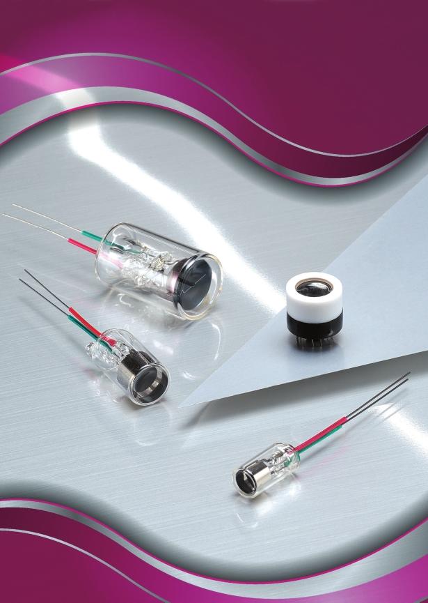
1 Phototubes
2 PHOTOTUBES FEATURES AND APPLICATIONS FEATURES High sensitivity and high stability Wide dynamic range Superior temperature stability Large photosensitive area Low voltage operation SPECTRAL RESPONSE RANGE AND APPLICATIONS Window Spectral Spectral Range Photocathode Material Response Typical Applications Spectral response in vacuum UV region only Vacuum UV region only Solar blind spectral response Wide spectral response from UV to infrared High sensitivity and high stability make phototubes very useful in chemical and medical analytical instruments which require high reliability. Phototubes feature a wide dynamic range from several picoamperes to several microamperes, providing signal output with excellent linearity. Phototubes show virtually no fluctuation with changes in the ambient temperature. Compared to semiconductor sensors, phototubes offer larger photosensitive area. Phototubes are designed to operate at a low voltage. Cs-I Diamond Au (single metal) Cs-Te Sb-Cs MgF MgF Borosilicate nm to 00 nm 0 nm to 00 nm nm to 0 nm 0 nm to 0 nm 0 nm to 0 nm 0 nm to 0 nm nm to 0 nm nm to 0 nm 00 nm to 0 nm q w e r t y u i o Vacuum UV spectrophotometer 7 nm monitor for excimer lamp nm monitor for sterilizing mercury lamp nm monitor for sterilizing mercury lamp Monitor for nm, nm mercury line spectrum Ozone monitor Spectrophotometer Blood analyzer Applicable Phototube Type No. R7 R7 R00U- R00U- R0 R7, R00U- R07, R, R00U-0 R0, R77 R GLOSSARY OF TERMS Spectral response characteristic: When light (photons) enters the photocathode, it is converted into electrons emitting from the photocathode at a certain ratio. This ratio depends on the wavelength of incident light. The relationship between the ratio and the wavelength is called spectral response characteristic. Peak wavelength: The wavelength gives the maximum sensitivity to the photocathode. In this catalog, the peak wavelength for radiant sensitivity (A/W) is listed. Absolute maximum ratings: The limiting values of the operating and environmental conditions applied to a phototube. Any conditions shall not exceed these ratings even instantaneously. Anode supply voltage: The voltage applied across the anode and the cathode. Normally, the cathode is used at ground potential, so the anode supply voltage equals the potential difference between the anode and ground. Peak cathode current: The peak current that can be allowed from the cathode when it is of pulse waveform. Average cathode current: The average current that can be allowed from the cathode. Normally, it is the average for 0 seconds. Average cathode current density: The average cathode current per unit surface area on the photocathode. Luminous sensitivity: The ratio of photocurrent in amperes (A) flowing in the photocathode to the incident luminous flux in lumens (lm). Current (A) Luminous sensitivity (A/lm) = Luminous flux (lm) Radiant sensitivity: The ratio of photocurrent in amperes (A) flowing in the photocathode to the intensity of the incident light in watts (W). Current (A) Radiant sensitivity (A/W) = Light intensity (W) Dark Current: The current flowing between the anode and the cathode when light is removed. Interelectrode capacitance: The electrostatic capacitance between the anode and the cathode. Recommended operating voltage: The lifetime of a phototube tends to become shortened as the supply voltage increases. The supply voltage should be made as low as possible as compared to the maximum ratings, in order to lengthen useful life. However, if the supply voltage is too low, the voltagecurrent characteristics fall outside the saturation region, and undersirable phenomena such as hysteresis (Note ) may occur. Considering these effects, the recommended operating voltage for each type of phototube is listed in this catalog. (Note ) Hysteresis: The temporary instability in output signal when light is applied to a phototube, showing "overshoot" or "undershoot" without being proportional to light input.
3 SPECTRAL RESPONSE CHARACTERISTICS 0 TPT B000ED RADIANT SENSITIVITY (ma/w) Cs-I_MgF Cs-I_ Diamond_MgF Diamond_ Au_ Cs-Te_ 7Cs-Te_ Sb-Cs_ 9Sb-Cs_Borosilicate WAVELENGTH (nm)
4 PHOTOTUBES CHARACTERISTICS Type No. GLASS BULB TYPE For Vacuum UV (Cs-I Photocathode) R7 R7 Spectral Response (nm) to 00 0 to 00 A Peak Wavelength (nm) 0 Outline Diagram No. For UV / High Power (Au Single Metal Photocathode) For UV / General Purpose (Cs-Te Photocathode) R07 R7 R to 0 0 to 0 to For UV to Visible (Sb-Cs Photocathode) R R0 R77 00 to 0 to 0 to METAL PACKAGE TYPE For Vacuum UV (Diamond Photocathode) For UV / General Purpose (Cs-Te Photocathode) e e q w w q w r Tube Diameter (mm) Photocathode Area Min. (mm) Input Window Material MgF Borosilicate glass Anode Supply Voltage (V) Absolute Maximum Ratings B Average Peak Cathode Average Cathode Current Cathode Current Density Current (µa) 0... (µa/cm ) (µa) Ambient Temperature ( C) C R0 0 to 0 e. 0. R00U- R00U- to 0 0 to 0 t t MgF R00U- R00U-0 0 to 0 to y u NOTE: ASee spectral response characteristics on page. BOutput current averaged over second time interval. The whole photocathode is uniformly illuminated. CWhen a tube is operated below - C see page, "Caution" DIMENSIONAL OUTLINES (Unit: mm) q R, R07 w R7, R, R0 e R7, R0, R7 r R77 PHOTO- MAX. MIN. PHOTO- 0 MAX. MIN. PHOTO-. MAX. MIN. PHOTO-. MAX. MIN. 0 MIN. MAX. 0 MAX. FLEXIBLE LEAD ANODE (RED) (GREEN) FLEXIBLE LEAD (GREEN) ANODE (RED) 7 ± MAX. 0 MIN. 0 MAX. ANODE (RED) (GREEN) FLEXIBLE LEAD 7 ± MAX. MAX. 0 MIN. FLEXIBLE LEAD (GREEN) ANODE (RED) MAX. MAX. 0 MIN. TPT A000EA TPT A000EB TPT A00EC TPT A000EB
5 Luminous Sensitivity Typ. (µa/lm) Min. (µa/lm) D Characteristics at C Radiant Sensitivity nm nm Pt Peak E Dark Current Typ. Min. Typ. Min. Typ. Min. Max. (ma/w) (ma/w) (ma/w) (ma/w) (ma/w) (ma/w) (pa) Recommended Operating Voltage (V) Interelectrode Capacitance (pf) Type No.. R7. R R0 0.0 R R R R 0 0. R R77 R00U- R00U R00U- R00U-0 DThe photocurrent from the photocathode per incident light flux (0 - to 0 - lumens) from a tungsten filament lamp operated at a distribution temperature of K. ESee peak wavelength. t R00U-, - y R00U- u R00U-0 MIN. MIN. EFFECTIVE AREA Top View MIN. EFFECTIVE AREA Top View EFFECTIVE AREA Top View PHOTO.9 ± 0. WINDOW.0 ± ± ± 0.. ± 0. (Teflon) (Polyoxymethylene) PHOTO.9 ± 0. WINDOW.0 ± ± ± 0.. ± 0. (Teflon) (Polyoxymethylene) PHOTO.9 ± 0. WINDOW 9. ± ± 0..0 ± 0.7. ± 0. (Polyoxymethylene). ± 0. Side View ±.0 ± 0.. ± 0. Side View ±.0 ± 0.. ± 0. Side View ±.0 ± 0. GUIDE MARK ANODE GUIDE MARK ANODE GUIDE MARK ANODE SHORT PIN.0 0. SHORT PIN.0 0. SHORT PIN SHORT PIN.0 0. Bottom View - 0. SHORT PIN.0 0. Bottom View - 0. SHORT PIN.0 0. Bottom View TPT A00EB TPT A00EB TPT A00EC NOTE: Don't use pins excepting ANODE and pins.
6 PHOTOTUBES EXAMPLE OF OPERATING CIRCUITS OPERATING CIRCUITS FOR PHOTOTUBES Figure shows an operating circuit example using the phototube bias voltage also for the power to an operational amplifier. The feedback resistance Rf should be chosen so that the output voltage becomes 0. V to V. Cf must be placed for stable operation and should be between 0 pf and pf. It is recommended to use a low-bias, low-offset-current FET input operational amplifier. For the input terminal (pin ), a guard pattern should be provided on the printed circuit board or a stand-off terminal made of Teflon should be used. Figure : When Pulse / Minus Powers Are Available Figure shows an operating circuit in which a low-impedance voltage is output from an operation amplifier after the signal current has been converted into a voltage through the road resistance RL. The operational amplifier should be a low-bias, low-offset-current type which can be operated on a single power. Figure : Operating Circuit Operating on Signal Power + V SIGNAL CURRENT Ip ANODE PHOTOTUBE GUARD + V PATTERN + Cf 7 OP AMP Rf OUTPUT VOLTAGE Eo=-Rf Ip SIGNAL CURRENT Ip ANODE RL PHOTOTUBE + 7 OP AMP GND OUTPUT VOLTAGE Eo=RL Ip GND (Impedance conversion circuit) - V TPT C000EC (Inverting current-voltage conversion circuit) TPT C000EC NOTE: The operational amplifiers that can be used in these circuits differ in such factors as operating temperature range, bias current, phase compensation, and offset adjustment method, depending on the type used. Please refer to the catalog or data sheet available from the manufacturer. Sample circuits listed in this catalog introduce typical applications and do not cover any guarantee of the circuit design. No patent rights are granted to any of the circuits described herein.
7 CAUTIONS Maximum ratings Always operate the phototube within the maximum rating listed in this catalog. The light input surface area should be as large as possible The output current available from a phototube is determined by the maximum average cathode current and maximum average cathode current density. If the light input surface area is small, even if the output current is below the maximum average cathode current, the maximum average cathode current density may be exceeded. Therefore, the light input surface area should be as large as possible to decrease the cathode current per unit surface area. This is important also, from the standpoint of photocathode uniformity (i.e., variation in sensitivity with respect to incident light position). Handle tubes with extreme care Phototubes have evacuated glass envelopes. Allowing the glass to be scratched or to be subjected to shock can cause cracks. Extreme care should be taken in handling, especially for tubes with graded sealing of synthetic silica. Avoid mechanical vibration Mechanical vibration can cause microphonic noise (sensitivity fluctuation caused by vibration of the electrode.) and variation in sensitivity caused by displacement of the incident light position. keep faceplate and base clean Do not touch the faceplate and base with bare hands. Dirt and fingerprints on the faceplate cause loss of transmittance and dirt on the base may cause ohmic leakage. Should they become soiled, wipe it clean using alcohol. Avoid direct sunlight and other high-intensity light Avoid subjecting the phototube to direct sunlight or other high-intensity light, as this can adversely affect the photocathode, causing not only loss of sensitivity but instability as well. Handling of tubes with a glass base A glass base (also called button stem) is weak, so care should be taken in handling this type of tube. Cooling of tubes When cooling a phototube, the photocathode section is usually cooled. However, if you suppose that the base is also cooled down to - C or below, please consult our sales office in advance. Helium permeation through silica bulb Helium will permeate through the silica bulb, leading to an increase in noise. Avoid operating or storing tubes in an environment where helium is present. Data and specifications listed in this catalog are subject to change due to product improvement and other factors. Before specifying any of the types in your production equipment, please consult our sales office. WARRANTY In general, Hamamatsu products listed in this catalog are warranted for a period of one year from time of delivery. This warranty is limited to replacement for the defective product. Note, however, that this warranty will not apply to failures caused by natural calamity or misuse. CE MARKING This catalog contains products which are subject to CE Marking of European Union Directives. For further details, please consult Hamamatsu sales offices.
8 PHOTOTUBES Subject to local technical requirements and regulations, availability of products included in this promotional material may vary. Please consult with our sales office. Information furnished by HAMAMATSU is believed to be reliable. However, no responsibility is assumed for possible inaccuracies or omissions. Specifications are subject to change without notice. No patent rights are granted to any of the circuits described herein. 0 Hamamatsu Photonics K.K. HAMAMATSU PHOTONICS K.K. HAMAMATSU PHOTONICS K.K., Electron Tube Division -, Shimokanzo, Iwata City, Shizuoka Pref., -09, Japan, Telephone: ()9/-, Fax: ()9/-0 U.S.A.: Hamamatsu Corporation: 0 Foothill Road, Bridgewater. N.J , U.S.A., Telephone: () , Fax: () usa@hamamatsu.com Germany: Hamamatsu Photonics Deutschland GmbH: Arzbergerstr. 0, D- Herrsching am Ammersee, Germany, Telephone: (9)-7-0, Fax: (9)- info@hamamatsu.de France: Hamamatsu Photonics France S.A.R.L.: 9, Rue du Saule Trapu, Parc du Moulin de Massy, 9 Massy Cedex, France, Telephone: () , Fax: () infos@hamamatsu.fr United Kingdom: Hamamatsu Photonics UK Limited: Howard Court, 0 Tewin Road, Welwyn Garden City, Hertfordshire AL7 BW, United Kingdom, Telephone: ()707-9, Fax: () info@hamamatsu.co.uk North Europe: Hamamatsu Photonics Norden AB: Torshamnsgatan SE- 0 Kista, Sweden, Telephone: () , Fax: () info@hamamatsu.se Italy: Hamamatsu Photonics Italia S.r.l.: Strada della Moia, int., 000 Arese (Milano), Italy, Telephone: (9)0-97, Fax: (9) info@hamamatsu.it China: Hamamatsu Photonics (China) Co., Ltd.: B0 Jiaming Center, No.7 Dongsanhuan Beilu, Chaoyang District, Beijing 00, China, Telephone: ()0--00, Fax: ()0-- hpc@hamamatsu.com.cn Taiwan: Hamamatsu Photonics Taiwan Co., Ltd.: F-, No., Section, Gongdao th Road, East District, Hsinchu, 00, Taiwan R.O.C. Telephone: () , Fax: () info@tw.hpk.co.jp TPT E0 MAY 0 IP
Phototubes. Phototubes, Solar Blind Phototubes and Biplanar Phototubes
 Phototubes Phototubes, Solar Blind Phototubes and Biplanar Phototubes FEATURES AND APPLICATIONS FEATURES AND APPLICATIONS OF PHOTOTUBES FEATURES High-speed response Choice of spectral response High sensitivity
Photosensitive area size (mm) Reverse voltage VR max (V) R to +60
 Reverse voltage VR max (V) R to +60") ,, 6 to 37 mm resistance length PSD for precision distance measurement Hamamatsu provides various types of one-dimensional PSD (position sensitive detector) designed for precision distance measurement
,, 6 to 37 mm resistance length PSD for precision distance measurement Hamamatsu provides various types of one-dimensional PSD (position sensitive detector) designed for precision distance measurement
Short wavelength type APD. Effective photosensitive area (mm) Effective photosensitive area size* 2
 Effective photosensitive area size* 2") Short wavelength type APD Features High sensitivity at visible range Low noise High gain Low capacitance Applications Low-light-level measurement Analytical instrument Structure / Absolute maximum ratings
Short wavelength type APD Features High sensitivity at visible range Low noise High gain Low capacitance Applications Low-light-level measurement Analytical instrument Structure / Absolute maximum ratings
Effective photosensitive area. Photosensitive area size
 High performance, high reliability Si PIN photodiodes The is a high-speed Si PIN photodiode having high sensitivity over a wide spectral range from visible to near infrared light. The provides high performance
Low bias operation, for 800 nm band
 Low bias operation, for 800 nm band These are 800 nm band near-infrared Si APDs that can operate at low voltages, 200 V or less. They are suitable for applications such as FSO (free space optics) and optical
Parameter Symbol Specification Unit Photosensitive area - ɸ0.8 mm Package mm
 Surface mount type, high-speed Si photodiode The is a Si PIN photodiode with sensitivities in the visible to near infrared range and is compatible with lead-free solder reflow. It features high-speed response
Peak emission wavelength: 3.9 μm
 Peak emission wavelength: 3.9 μm The is a high-output mid-infrared LED with a 3.9 µm peak emission wavelength. It is a product that has been achieved using Hamamatsu unique crystal growth technology and
Photo IC diode. Plastic package shaped the same as metal package. S SB. Features. Applications
 Plastic package shaped the same as metal package The photo IC has spectral response close to human eye sensitivity. Two photosensitive areas are made on a single chip. Almost only the visible range can
MPPC modules. MPPC array modules for very-low-level light detection, 16 ch analog output. C13368/C13369 series (Analog output type)
") MPPC modules C13368/C13369 series (Analog output type) MPPC array modules for very-low-level light detection, 16 ch analog output The C13368/C13369 series (analog output type) is an optical measurement
MPPC modules C13368/C13369 series (Analog output type) MPPC array modules for very-low-level light detection, 16 ch analog output The C13368/C13369 series (analog output type) is an optical measurement
Effective photosensitive area (mm)
") Chip carrier package for mount The, S5107, and S7510 are Si PIN photodiodes sealed in chip carrier packages suitable for mount using automated solder reflow techniques. These photodiodes have large photosensitive
Chip carrier package for mount The, S5107, and S7510 are Si PIN photodiodes sealed in chip carrier packages suitable for mount using automated solder reflow techniques. These photodiodes have large photosensitive
Effective photosensitive area (mm) Photosensitive area size
 Photosensitive area size") High UV resistance, photodiodes for UV monitor The are Si photodiodes that have achieved high reliability for monitoring ultraviolet light by employing a structure that does not use resin. They exhibit
High UV resistance, photodiodes for UV monitor The are Si photodiodes that have achieved high reliability for monitoring ultraviolet light by employing a structure that does not use resin. They exhibit
InGaAs PIN photodiode arrays
 16/32/46 element InGaAs array for near IR detection The is one-dimensional InGaAs PIN photodiode array in a ceramic DIP (dual inline package). It can be used to perform simple spectroscopic analysis. Features
Operating Instructions for PMT Tube P3
 Discovery Way, Acton, MA 07 Phone: (97)3-3, Fax: (97)3-0 Web Site: www.piacton.com Operating Instructions for PMT Tube P3 Ver.0 PHOTOMULTlPLlER TUBE R mm (-/ Inch) Transmission Mode S Photocathode, Side
New product of near infrared (to 900 nm) detection
 detection") WITH THERMOELECTRIC COOLER H7844 New product of near infrared (to 900 nm) detection FEATURES A newly developed high sensitivity multialkali side-on photomultiplier tube Fast cooling (3 minutes) by thermoelectric
WITH THERMOELECTRIC COOLER H7844 New product of near infrared (to 900 nm) detection FEATURES A newly developed high sensitivity multialkali side-on photomultiplier tube Fast cooling (3 minutes) by thermoelectric
InAsSb photovoltaic detectors
 High-speed response and high sensitivity in the spectral band up to 11 μm Infrared detectors The are photovoltaic type infrared detectors that have achieved high sensitivity in the spectral band up to
Optics modules. Absorbance measurement module with built-in photodiode array, optical elements, current-tovoltage. C13398 series.
 Absorbance measurement module with built-in photodiode array, optical elements, current-tovoltage converter, etc. The is an optics module for absorbance measurement featuring high blocking performance
Application OCT. Dimensions (mm) Weight (g) Operating temperature* 1 Storage temperature* 1 λ=1.55 μm (V) (mw)
 Weight (g) Operating temperature* 1 Storage temperature* 1 λ=1.55 μm (V) (mw)") Balanced detectors with reduced multiple reflections These are differential amplification type photoelectric conversion modules containing two Hamamatsu photodiodes with balanced characteristics. The photodiodes
Balanced detectors with reduced multiple reflections These are differential amplification type photoelectric conversion modules containing two Hamamatsu photodiodes with balanced characteristics. The photodiodes
InAsSb photovoltaic detector
 InAsSb photovoltaic detector P12691-21 High-speed response and high sensitivity in the 8 μm spectral band Thermoelectrically cooled infrared detector with no liquid nitrogen required The P12691-21 is an
UV-LED MODULE. UV Irradiation Intensity Distribution Graphs
 UV-LED MODULE UV Irradiation Intensity Distribution Graphs Product Lineup Lens Lineup Product Lineup LED DRIVER C1559-1 LED HEAD UNIT L1561/L196 SERIES standard type standard type high power type high
Parameter Specification Unit Photosensitive area mm Package Glass epoxy - Seal material Silicone resin -
 COB type, applicable to lead-free solder reflow The is a for visible to near infrared range and is compatible with lead-free solder reflow processes. The small and thin leadless package allows reducing
MPPC (Multi-Pixel Photon Counter)
") S13362-35DG Significantly reduced crosstalk, low afterpulses The can reduce dark count by cooling in addition to low afterpulses and low crosstalk of the S1336 series. The integrates the S1336 series with
S13362-35DG Significantly reduced crosstalk, low afterpulses The can reduce dark count by cooling in addition to low afterpulses and low crosstalk of the S1336 series. The integrates the S1336 series with
InAsSb photovoltaic detectors
 High-speed response and high sensitivity in the spectral band up to 5 μm Infrared detectors The are photovoltaic type infrared detectors that have achieved high sensitivity in the spectral band up to 5
Effective photosensitive* 2 area size. Storage temperature Tstg (mm) ( C) ( C) S φ0.2 φ0.5 S φ to to +100 S9075
 ( C) ( C) S φ0.2 φ0.5 S φ to to +100 S9075") /-05/-10, S5344, S5345 Short wavelength type APD, for 600 nm band These are short wavelength APDs with improved sensitivity in the UV to visible range. They offer high gain, high sensitivity, and low noise
/-05/-10, S5344, S5345 Short wavelength type APD, for 600 nm band These are short wavelength APDs with improved sensitivity in the UV to visible range. They offer high gain, high sensitivity, and low noise
Signal processing circuit for 1-D PSD
 Signal processing circuit for 1-D PSD Circuit board for easier 1-D PSD operation The is a DC signal processing circuit for one-dimensional PSD. It is suitable for displacement measurements using DC light.
Signal processing circuit for 1-D PSD
 Signal processing circuit for 1-D PSD Circuit board for easier 1-D PSD operation The is a DC signal processing circuit for one-dimensional PSD. It is suitable for displacement measurements using DC light.
Reverse voltage VR max. Electrical and optical characteristics (Typ. Ta=25 C, unless otherwise noted) Short. Temp. S coefficient (A/W) of
 Short. Temp. S coefficient (A/W) of") Ceramic package photodiodes with low dark current The are ceramic package photodiodes that offer low dark current. Ceramic package used is light-impervious, so no stray light can reach the photosensitive
Ceramic package photodiodes with low dark current The are ceramic package photodiodes that offer low dark current. Ceramic package used is light-impervious, so no stray light can reach the photosensitive
Non-discrete position sensors utilizing photodiode surface resistance
 Twodimensional PSD Nondiscrete position sensors utilizing photodiode surface resistance PSD (position sensitive detector) is an optoelectronic position sensor utilizing photodiode surface resistance. Unlike
These Si photodiodes have sensitivity in the UV to near IR range. They are suitable for low-light-level detection in analysis and the like.
 UV to near IR for precision photometry These Si photodiodes have sensitivity in the UV to near IR range. They are suitable for low-light-level detection in analysis and the like. Features High sensitivity
1-D PSD with small plastic package
 1D PSD with small plastic package Hamamatsu offers a variety of 1D PSDs (position sensitive detectors) molded into plastic packages. These PSDs feature excellent position detection resolution, high resistance
Parameter Specification Unit Photosensitive area mm Package Glass epoxy - Seal material Epoxy resin -
 COB type, applicable to lead-free solder reflow The is a Si PIN photodiode for visible to near infrared range and is compatible with lead-free solder reflow processes. The small and thin leadless package
Photosensor with front-end IC
 Compact APD suitable for various light level detection The is a compact optical device that integrates a Si APD and preamp. It has a built-in DC feedback circuit for reducing the effects of background
Photo IC diode. Plastic package shaped the same as metal package. S SB. Absolute maximum ratings (Ta=25 C)
") Plastic package shaped the same as metal package The photo IC has spectral response close to human eye sensitivity. Two photosensitive areas are made on a single chip. Almost only the visible range can
Plastic package shaped the same as metal package The photo IC has spectral response close to human eye sensitivity. Two photosensitive areas are made on a single chip. Almost only the visible range can
Si PIN photodiodes. High-speed detectors with plastic package. Structure. Absolute maximum ratings
 High-speed detectors with plastic package The and are high-speed APC (auto power control) detectors developed for monitoring laser diodes with a peak wavelength of 66 nm or 78 nm. The is designed for surface
Signal processing circuit for 2-D PSD
 Signal processing circuit for 2-D PSD Circuit board for easier 2-D PSD operation The is a DC signal processing circuit for two-dimensional PSD. It is suitable for displacement measurements using DC light.
Reduced color temperature errors
 Reduced color temperature errors The is a photo IC diode with spectral response characteristics that closely resemble human eye sensitivity. Two active areas are formed on the same chip, and the outputs
Signal processing circuit for 2-D PSD
 Signal processing circuit for 2-D PSD Circuit board for easier 2-D PSD operation The is a DC signal processing circuit for two-dimensional PSD. It is suitable for displacement measurements using DC light.
Accessories for infrared detector
 Temperature controllers Heatsinks for TE-cooled detector Chopper, etc. Wide lineups of accessories for infrared detector HAMAMATSU provides temperature controllers, heatsinks for TE-cooled detector, chopper
Si photodiode. Applicable to lead-free solder reflow and wide temperature range. S9674. Absolute maximum ratings
 Applicable to lead-free solder reflow and wide temperature range The is a photodiode that is applicable to lead-free solder reflow and has an extremely wide operating and storage temperature range (-40
Photon counting module
 Photon counting module Fiber coupling type, low-light-level detection The is a photon counting module that can detect low-level light. It consists of a TE-cooled single pixel photon counter (SPPC), signal
16-element Si photodiode arrays
 Back-illuminated photodiode arrays for X-ray nondestructive inspection (element pitch: mm) The is a back-illuminated type 16-element photodiode array specifically designed for non-destructive X-ray inspection.
Suppressed IR sensitivity
 For UV to visible, precision photometry; suppressed IR sensitivity These Si photodiodes have suppressed IR sensitivity. They are suitable for low-light-level detection in analysis and the like. Features
Applications. Photosensitive area size. Storage temperature Tstg (mm) (mm 2 ) (V) ( C) ( C) S
 (mm 2 ) (V) ( C) ( C) S") , etc. Photodiodes molded into clear plastic packages These are Si photodiodes molded into clear plastic packages. Two types are available with sensitivity in the visible range and in the visible to near
, etc. Photodiodes molded into clear plastic packages These are Si photodiodes molded into clear plastic packages. Two types are available with sensitivity in the visible range and in the visible to near
16-element Si photodiode arrays
 Back-illuminated photodiode arrays for X-ray nondestructive inspection (element pitch: mm) The is a back-illuminated type 16-element photodiode array specifically designed for non-destructive X- ray inspection.
Photo IC diode. Wide operating temperature: -40 to +105 C. S MT. Absolute maximum ratings (Ta=25 C)
") Wide operating temperature: -40 to +05 C The photo IC has a spectral response close to human eye sensitivity. Two active areas are made on a single chip. Almost only the visible range can be measured by
Wide operating temperature: -40 to +05 C The photo IC has a spectral response close to human eye sensitivity. Two active areas are made on a single chip. Almost only the visible range can be measured by
M=100, RL=50 Ω λ=800 nm, -3 db
 Low bias operation, for 800 nm band, small package Features Miniature and thin package:.8 3..0 t mm Stable operation at low bias High-speed response High sensitivity Low noise Applications Optical rangefinder
Si PIN photodiodes. High-speed detectors with plastic package. Structure. Absolute maximum ratings
 High-speed detectors with plastic package The and are high-speed APC (auto power control) detectors developed for monitoring laser diodes with a peak wavelength of 66 nm or 78 nm. The is designed for surface
RGB color sensor. Effective photosensitive area. Green, Red: 2.25 Blue : 4.5
 Si photodiodes S6428-01 S6429-01 S6430-01 RGB color sensor The S6428-01, S6429-01 and S6430-01 are color sensors designed to respectively detect monochromatic colors of blue (λp=460 nm), green (λp=540
Power supply for MPPC
 Power supply for MPPC C1104-0 Bias power supply with built-in high precision temperature compensation for MPPCs The C1104-0 is a high voltage power supply that is optimized for MPPCs (multi-pixel photon
Peak emission wavelength: 4.3 μm
 Peak emission wavelength: 4.3 μm The is a mid infrared LED with a 4.3 μm peak emission wavelength. It is a product that has been achieved using Hamamatsu unique crystal growth technology and process technology.
Applications. l Image input devices l Optical sensing devices
 IMAGE SENSOR CMOS linear image sensor S8377/S8378 series Built-in timing generator and signal processing circuit; single 5 V supply operation S8377/S8378 series is a family of CMOS linear image sensors
APD modules. Operates an APD with single 5 V supply (standard type, short-wavelength type) C12702 series.
 C12702 series.") Operates an APD with single 5 V supply (standard type, short-wavelength type) Features Includes a high-sensitivity APD Uses a Hamamatsu high-sensitivity Si APD. Four types are available with different
Operates an APD with single 5 V supply (standard type, short-wavelength type) Features Includes a high-sensitivity APD Uses a Hamamatsu high-sensitivity Si APD. Four types are available with different
CMOS linear image sensors
 Built-in timing generator and signal processing circuit; 5 V single supply operation The is a family of CMOS linear image sensors designed for image input applications. These linear image sensors operate
Artisan Technology Group is your source for quality new and certified-used/pre-owned equipment
 Artisan Technology Group is your source for quality new and certified-used/pre-owned equipment FAST SHIPPING AND DELIVERY TENS OF THOUSANDS OF IN-STOC ITEMS EQUIPMENT DEMOS HUNDREDS OF MANUFACTURERS SUPPORTED
Driver circuit for MPPC
 Simple evaluation starter kit for non-cooled s The is a starter kit designed for simple non-cooled evaluations. It consists of a sensor board and a power supply board. The sensor board includes an socket
MCT photoconductive detectors
 MCT photoconductive detectors P3257 series P4249-08 0 μm band infrared detector with high sensitivity and high-speed response Features High-speed response, high sensitivity in the 0 μm band detection Photoconductive
Driver circuit for InGaAs linear image sensor
 (G11135 series, G14006-512DE) The is a driver circuit developed for InGaAs linear image sensors (G11135 series, G14006-512DE). The driver circuit consists of an analog video signal processing circuit (16-bit
InAsSb photovoltaic detector
 InAsSb photovoltaic detector P2-2 High-speed response and high sensitivity in the 5 μm spectral band Thermoelectrically cooled infrared detector with no liquid nitrogen required The P2-2 is an infrared
Infrared detector modules with preamp
 Easy-to-use detector modules with built-in preamps Infrared detector modules operate just by connecting to DC power supplies. The detector element is selectable from among InGaAs, InAs, InSb, and InAsSb
MPPC (Multi-Pixel Photon Counter)
") MPPC (Multi-Pixel Photon Counter) MPPCs in a chip size package miniaturized through the adoption of TSV structure The are MPPCs for precision measurement miniaturized by the use of TSV (through-silicon
MPPC (Multi-Pixel Photon Counter) MPPCs in a chip size package miniaturized through the adoption of TSV structure The are MPPCs for precision measurement miniaturized by the use of TSV (through-silicon
PbSe photoconductive detectors
 PbSe photoconductive detectors P9696 series P327-8 Infrared detectors with fast response and high sensitivity in 5 μm wavelength band Compared to other detectors used in the same wavelength regions, PbSe
Between elements measure. Photosensitive area (per 1 element)
") 16, 35, 46 element Si photodiode array for UV to NIR The are Si photodiode linear array mounted in ceramic DIPs (Dual Inline Packages). These photodiode arrays are primarily developed for low-light-level
16, 35, 46 element Si photodiode array for UV to NIR The are Si photodiode linear array mounted in ceramic DIPs (Dual Inline Packages). These photodiode arrays are primarily developed for low-light-level
APD modules. APD module integrated with peripheral circuits. C12703 series. Selection guide. Block diagram
 APD module integrated with peripheral circuits Features Uses a high sensitivity APD Two types of APDs with different photosensitive areas (φ1.5 mm, φ3. mm) are provided. On-board high sensitivity circuit
Photo IC diode. COB (chip on board) type, small package. S CT. Absolute maximum ratings
 type, small package. S CT. Absolute maximum ratings") COB (chip on board) type, small package mm The photo IC has spectral response close to human eye sensitivity. Two photosensitive areas are made on a single chip. Almost only the visible range can be measured
COB (chip on board) type, small package mm The photo IC has spectral response close to human eye sensitivity. Two photosensitive areas are made on a single chip. Almost only the visible range can be measured
Photodiode modules. C10439 series. Integrates photodiode for precision photometry with low-noise amp.
 Integrates photodiode for precision photometry with low-noise amp The photodiode modules are high-precision photodetectors that integrate a photodiode and a current-to-voltage amplifier. The output from
MPPC (multi-pixel photon counter)
") MPPC (multi-pixel photon counter) Low afterpulses, wide dynamic range, for high-speed measurement Photosensitive area: 1 1 mm These MPPCs utilize very small pixels arrayed at high densities to achieve
MPPC (multi-pixel photon counter) Low afterpulses, wide dynamic range, for high-speed measurement Photosensitive area: 1 1 mm These MPPCs utilize very small pixels arrayed at high densities to achieve
High-speed photodiodes (S5973 series: 1 GHz)
") S5973 series High-speed photodiodes (S5973 series: 1 GHz), and S5973 series are high-speed Si PIN photodiodes designed for visible to near infrared light detection. These photodiodes provide wideband characteristics
S5973 series High-speed photodiodes (S5973 series: 1 GHz), and S5973 series are high-speed Si PIN photodiodes designed for visible to near infrared light detection. These photodiodes provide wideband characteristics
Applications. Number of terminals. Supply voltage (op amp) Vcc
 Vcc") PHOTODIODE Si photodiode with preamp S5590, S559 Photodiode and preamp integrated with feedback resistance and capacitance S5590, S559 are lownoise light sensors consisting of a large area Si photodiode,
PHOTODIODE Si photodiode with preamp S5590, S559 Photodiode and preamp integrated with feedback resistance and capacitance S5590, S559 are lownoise light sensors consisting of a large area Si photodiode,
MCT photoconductive detectors
 Non-cooled type and suitable for long, continuous operation Features Choice of spectral response (up to 12 μm) The band gap can be adjusted by controlling the composition ratio of HgTe and CdTe. Utilizing
Mini-spectrometer. SMD series C14384MA-01. High sensitivity in the near infrared region (to 1050 nm), ultra-compact grating type spectrometer
, ultra-compact grating type spectrometer") Mini-spectrometer SMD series C14384MA-01 High sensitivity in the near infrared region (to 1050 nm), ultra-compact grating type spectrometer The C14384MA-01 is a ultra-compact grating type spectrometer
Mini-spectrometer SMD series C14384MA-01 High sensitivity in the near infrared region (to 1050 nm), ultra-compact grating type spectrometer The C14384MA-01 is a ultra-compact grating type spectrometer
Compact size (16 mm diameter, 12 mm seated length), Fast Time response (rise time 0.78 ns)
, Fast Time response (rise time 0.78 ns)") METAL ACKAGE HOTOMULTILIER TUBE R7400U SERIES Compact size (6 mm diameter, 2 mm seated length), Fast Time response (rise time 0.7 ns) The R7400U series is a subminiature photomultiplier tube with a 6 mm
METAL ACKAGE HOTOMULTILIER TUBE R7400U SERIES Compact size (6 mm diameter, 2 mm seated length), Fast Time response (rise time 0.7 ns) The R7400U series is a subminiature photomultiplier tube with a 6 mm
16-element Si photodiode arrays
 S11212-421 S11212-321 S11212-021 S11212-121 Back-illuminated photodiode arrays for non-destructive inspection The is a back-illuminated type 16-element photodiode array specifically designed for non-destructive
Photo IC for optical switch
 Photo IC with optical switch functions The S6841 and S8119 are specifically designed for optical switches. A transmission mode or reflection mode optical switch can be easily configured when used in combination
Near infrared image sensor (0.9 to 1.7 µm) with high-speed data rate
 with high-speed data rate") IMAGE SENSOR InGaAs linear image sensor G99-56D/-5D Near infrared image sensor (.9 to.7 µm) with high-speed data rate HAMAMATSU provides high-speed, near infrared image sensors designed for detectors used
IMAGE SENSOR InGaAs linear image sensor G99-56D/-5D Near infrared image sensor (.9 to.7 µm) with high-speed data rate HAMAMATSU provides high-speed, near infrared image sensors designed for detectors used
Peak sensitivity wavelength λp (nm) Photosensitive area (mm)
 Photosensitive area (mm)") Integrates a -PSD for precision photometry or a 4-segment Si photodiode with low-noise amp in a compact case PSD modules contain a high-precision two-dimensional PSD (position sensitive detector) or a
Integrates a -PSD for precision photometry or a 4-segment Si photodiode with low-noise amp in a compact case PSD modules contain a high-precision two-dimensional PSD (position sensitive detector) or a
Power supply for MPPC
 Power supply for MPPC C1104-0 Bias power supply with built-in high precision temperature compensation for MPPCs The C1104-0 is a high voltage power supply that is optimized for MPPCs (multi-pixel photon
Driver circuit for InGaAs linear image sensor
 Driver circuit for InGaAs linear image sensor [G11620 series (non-cooled type)] The is a driver circuit developed for InGaAs linear image sensors [G11620 series (non-cooled type)]. The driver circuit consists
APD module. Variable gain, stable detection even at high gain. C Applications. Features. Sensitivity vs.
 APD module C158-1 Variable gain, stable detection even at high gain The C158-1 consists of an APD, current-to-voltage converter, high-voltage power supply circuit as well as a microcontroller for compensating
Variable gain and stable detection even at high gains
 MODULE APD module C5 Variable gain and stable detection even at high gains Along with an APD, current-to-voltage conversion circuit, and high-voltage power supply circuit, the C5 contains a microcontroller
Driver circuit for CMOS linear image sensor
 High-precision driver circuit with variable integration time function The is a driver circuit specifically designed for the Hamamatsu S10111 to S10114 series, S10121 to S10124 series (-01) current-output
Photosensitive area (mm) 4 4. Peak sensitivity wavelength (nm) Supply voltage Dark state. Max. Vcc max. Tstg Min. Max. (ma) (V)
 4 4. Peak sensitivity wavelength (nm) Supply voltage Dark state. Max. Vcc max. Tstg Min. Max. (ma) (V)") Integrates a PSD for precision photometry or a 4-segment Si photodiode with low-noise amp in a compact case PSD modules contain a high-precision two-dimensional PSD (position sensitive detector) or a 4-segment
Integrates a PSD for precision photometry or a 4-segment Si photodiode with low-noise amp in a compact case PSD modules contain a high-precision two-dimensional PSD (position sensitive detector) or a 4-segment
InGaAs multichannel detector head
 Near infrared line camera (Line rate: 31.25 khz) The is a multichannel detector head suitable for applications where high-speed response is required, such as SD- OCT (spectral domain-optical coherence
CMOS linear image sensor
 Digital output, built-in 8/10-bit A/D converter, single power supply operation The is a CMOS linear image sensor designed for image input applications. The signal processing circuit has a charge amplifier
InGaAs linear image sensors
 Near infrared image sensors for portable analytical instruments The compact low-cost near infrared linear image sensors are designed for portable analytical instruments. They consume less current than
NMOS linear image sensor
 Image sensor highly sensitive to X-rays from 0 k to 00 kev s are self-scanning photodiode arrays designed specifically as detectors for multichannel spectroscopy. The scanning circuit is made up of N-channel
CMOS linear image sensor
 High sensitivity, photosensitive area with minute pixels The is a high sensitivity CMOS linear image sensor using a photosensitive area with minute pixels. It has a long photosensitive area (effective
16-element Si photodiode arrays
 S11299-321 S11299-421 S11299-21 S11299-121 Back-illuminated photodiode arrays for X-ray non-destructive inspection, slender board type The is a back-illuminated type 16-element photodiode array specifically
Driver circuit for CMOS linear image sensor
 Driver circuit for CMOS linear image sensor C13015-01 For CMOS linear image sensor S11639-01, etc. The C13015-01 is a driver circuit developed for Hamamatsu CMOS linear image sensor S11639-01, etc. By
Driver circuit for CCD linear image sensor
 For CCD image sensor (S11151-2048) The is a driver circuit designed for Hamamatsu CCD image sensor S11151-2048. The can be used in spectrometers when combined with the S11151-2048. The holds a CCD driver
CMOS linear image sensor
 CMOS linear image sensor S14739-20 High sensitivity, photosensitive area with vertically long pixels The S14739-20 is a high sensitivity CMOS linear image sensor using a photosensitive area with vertically
Distance linear image sensor
 Measures the distance to an object by TOF (time-of-flight) method The distance image sensor is designed to measure the distance to an object by TOF method. When used in combination with a pulse modulated
Driver circuits for CCD image sensor
 Driver circuit for CCD image sensor (S10420/S11071/S11510 series) The and are driver circuits designed for HAMAMATSU CCD image sensor S10420/S11071/S11510 series. The and can be used in spectrometer when
InGaAs linear image sensors
 Wide spectral response range, near infrared image sensors (0.5 to 1.7 μm) The InGaAs linear image sensors are specifically designed for near infrared multichannel spectrophotometry. The consists of an
Artisan Technology Group is your source for quality new and certified-used/pre-owned equipment
 Artisan Technology Group is your source for quality new and certified-used/pre-owned equipment FAST SHIPPING AND DELIVERY TENS OF THOUSANDS OF IN-STOCK ITEMS EQUIPMENT DEMOS HUNDREDS OF MANUFACTURERS SUPPORTED
MPPC (Multi-Pixel Photon Counter) arrays
 arrays") MPPC (Multi-Pixel Photon Counter) arrays MPPC arrays in a chip size package miniaturized through the adoption of TSV structure The is a MPPC array for precision measurement miniaturized by the use of TSV
MPPC (Multi-Pixel Photon Counter) arrays MPPC arrays in a chip size package miniaturized through the adoption of TSV structure The is a MPPC array for precision measurement miniaturized by the use of TSV
TM series TM-UV/VIS-MOS
 C12MD C13MD For UV to near IR, integrating optical system, and circuit mini-spectrometers are polychromators integrated with optical elements, an and a driver circuit. Two models are available: C12MD (TM-UV/VIS-MOS)
CMOS linear image sensor
 High sensitivity, photosensitive area with vertically long pixels The is a high sensitivity CMOS linear image sensor using a photosensitive area with vertically long pixels (14 200 μm). Other features
Mini-spectrometer. TF series. Compact and thin, built-in high-sensitivity CMOS image sensor for Raman spectroscopy C14214MA. Applications.
 TF series C14214MA Compact and thin, built-in high-sensitivity CMOS for Raman spectroscopy The mini-spectrometer TF series is a polychromator provided in a compact, thin case that houses optical elements,,
MPPC modules. Photon counting module with built-in MPPC. C series C10751 series. Selection guide
 C10507-11 series C10751 series Photon counting module with built-in MPPC The MPPC (multi-pixel photon counter) module is a photon counting module capable of low-light-level detection. This module consists
S P. Ultra-miniature, high performance Electromagnetically driven laser scanning MEMS mirror. Features.
 Si MEMS photodiode mirror Ultra-miniature, high performance Electromagnetically driven laser scanning MEMS mirror The is an electromagnetically driven mirror that incorporates our unique MEMS (micro-electro-mechanical
mini-spectrometer TG series Long-wavelength type (to 2.55 μm) nearinfrared C11118GA Optical characteristics (Ta=25 C)
 nearinfrared C11118GA Optical characteristics (Ta=25 C)") Long-wavelength type (to 2.55 μm) nearinfrared mini-spectrometer Hamamatsu mini-spectrometers are polychromators integrated with optical elements and an. Light to be measured is guided into the entrance
Long-wavelength type (to 2.55 μm) nearinfrared mini-spectrometer Hamamatsu mini-spectrometers are polychromators integrated with optical elements and an. Light to be measured is guided into the entrance