Nova NanoSEM Superior Imaging and Analytical Performance
|
|
|
- Julian McGee
- 5 years ago
- Views:
Transcription


1 Nova NanoSEM Superior Imaging and Analytical Performance
2
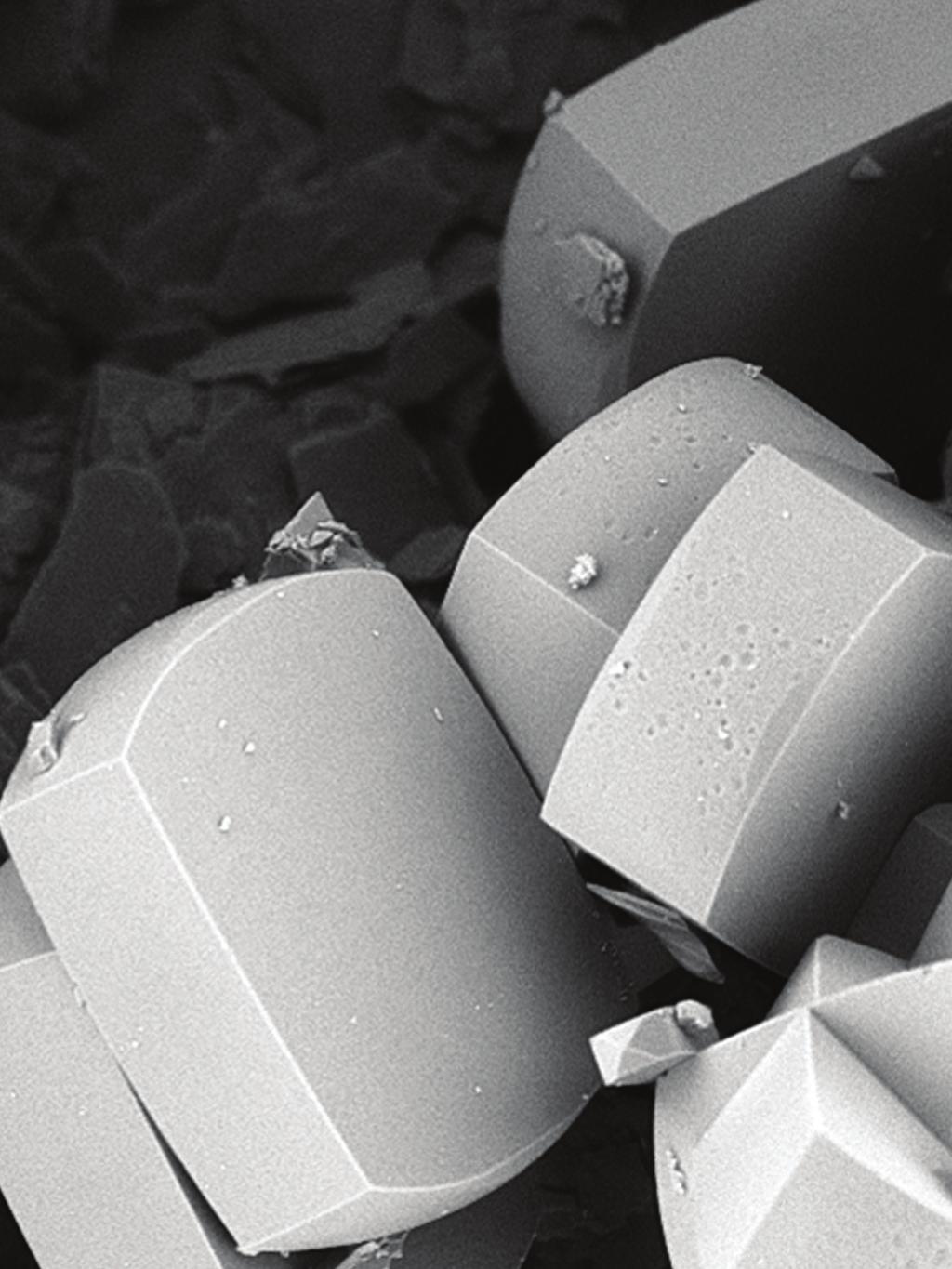
3 FEI Nova NanoSEM scanning electron microscopes combine best-in-class imaging with superb analytical performance in one easy-to-use instrument. Specifically designed to simplify laboratory operations, the Nova NanoSEM enables you to increase productivity without compromising the image and analytical quality that you demand. Gain an Advantage Outstanding imaging. Powerful analytics. All combined with unmatched ease of use and performance to give you a research advantage. Zeolite particles imaged in high-vacuum mode with charge filtering. Recent applications of zeolite particles include catalytic cracking and refining, and purifying natural gas and petroleum chemicals. 3


 resolution Powerful analysis. Gain top-quality analytical data on samples in high-vacuum mode and 1.")
![8 nm resolution in low-vacuum including glass, ceramics, and other non-conductive materials with mode when using low-voltage [1 kv]](/docs-images/90/103482463/images/4-3.jpg "operation. Gain the benefits high performance in low-vacuum mode. of low-vacuum imaging with sub 2 nm resolution. Gold on carbon.")
4 Research with No Compromises Most SEMs are designed to deliver high-performance imaging or high-performance analytics. With the FEI Nova NanoSEM, you can have both. The Nova NanoSEM allows you to easily switch instrument conditions based on sample type or the type of analysis you want to perform. Expand your research capabilities and achieve better answers with access to the most comprehensive information available. And, ultimately, achieve better research results. Best of Both Worlds High-resolution imaging. Achieve 1.4 nanometer (nm) resolution Powerful analysis. Gain top-quality analytical data on samples in high-vacuum mode and 1.8 nm resolution in low-vacuum including glass, ceramics, and other non-conductive materials with mode when using low-voltage [1 kv] operation. Gain the benefits high performance in low-vacuum mode. of low-vacuum imaging with sub 2 nm resolution. Gold on carbon. Sample imaged in high-vacuum mode achieving better than 1.4 nm resolution. 4 Ceramic sample. Low-vacuum EDX map showing Zirconium rich areas. Ceramic sample. High-resolution image acquired in low-vacuum mode.


 of")
5 High-resolution bright field STEM image of a NiTiZr shape memory alloy. This material is a lightweight, solid-state alternative to conventional actuators such as hydraulic, pneumatic, and motor-based systems. Superior image quality. Achieve high image quality across a wide range of samples. Accelerate EDS/EBSD/CL/analytical research with high-current beam and high resolution at both high and low voltages. EDX map. High-resolution map acquired in 30 seconds using > 100 nanoamperes (na) of beam current. Titanium oxide nanotubes. Highresolution image acquired at 2 kv. Shape memory alloy. Bright field STEM image. 5


6 It s Easy to Use The Nova NanoSEM allows researchers to achieve high-performance SEM analysis regardless of their experience level. Every researcher not only the microscopists can easily repeat analysis, acquire an accurate measurement, and characterize samples. Ease of use also enables researchers to maximize their research time. The Nova NanoSEM simplifies the process of setting parameters and swapping detectors, and it eliminates the need to coat samples, increasing productivity and optimizing precious time on an instrument. Optimize Productivity 6 Point-and-shoot functionality. Smart presets allow rapid data Quick save and recall. Tailor presets to users preferences, save them, acquisition to provide answers quickly. and quickly recall them to save time and improve repeatability. DCFI. Automatic real-time alignment of each frame during integration ensures that no drift effects are present when imaging challenging samples or when imaging in difficult environments. Quick presets. For example, operators can switch from SE + BSE imaging to four simultaneous images from the DBS detector using simple presets for screen layout and imaging conditions tailored to individual needs.


7 Ceramic coating on steel imaged at 2 kv. SEM imaging of ceramic coatings can provide insight into failure mechanisms, crack formation and analysis, and coating conformity as well as identify the phases present. Automatically align and calibrate. Optimize laboratory productivity by quickly making the system ready for the next user and application. Smart navigation features. The Nav-Cam automatically links the macro scale with the nano scale to ensure that the operator is never lost in the sample. Smart features simplify repeat analysis and reduce time spent on navigation by 15 to 20 percent. Simplified organization. Arrange user presets by sample type, operator, and application to control analysis quality and help ensure replicable results even with multiple operators and differing experience levels. User Interface. Optimizing imaging conditions on difficult samples, such as this easily charging uncoated chalk, is achieved easily. An operator can reference a new preset and achieve optimal results with a single click of a mouse. Slow scanning (left image) shows charge buildup, while interlaced scanning (right image) allows for the charge to dissipate, achieving optimal charge-free imaging in a single click. 7


8 Best-in-Class Performance Nova NanoSEM is precisely designed to deliver the highest quality results in the least amount of time. With materials that are sensitive to beam damage or contamination, the Nova NanoSEM maximizes the amount of data captured per scan before the sample becomes unusable. For example, with functionalized Zinc Oxide nanorods, data delivered by the Nova NanoSEM s superior imaging and analysis features help answer questions such as What is the size and distribution of catalyst particles on the nanorods? Sensitivity with Flexibility 8 Powerful beam deceleration technology. Achieve high Advanced detection system. Collect more information than resolution with low beam currents, minimizing damage traditional SEM instruments. FEI s proprietary DBS detector captures to sensitive samples. information from every angle to make every electron count. Mesoporous silica. Bright field STEM image showing 4 nm pores together with catalyst particles. Hydroxyapatite. Four individual images of ceramic coating on steel acquired simultaneously using the DBS detector. Topographic, material, and orientation contrasts all easily achieved.


9 Zinc Oxide Nanorods with Palladium particles on the surface imaged at 500 V in high vacuum. The addition of Palladium increases the sensitivity to hydrogen for sensor applications. Configuration flexibility. From high vacuum to low vacuum and high voltage to low voltage, get the sharpest, high-contrast, low-noise images over a full range of real-world samples. Gaseous analytical detector (GAD). Allows for high-resolution BSE imaging and analysis of these catalyst particles in low vacuum. Nova NanoSEM. Superior imaging and analytical performance. AI203. This is an ultrahigh-resolution image of the surface of AI203 acquired in low vacuum with the FEI Helix detector. 9
 detector simplifies interpretation of various contrast mechanisms.")


10 Technology Innovation Enhances Performance FEI technology innovation gives the Nova NanoSEM unique capabilities that enhance performance and deliver reliable, accurate results that other SEM systems cannot match. Directional backscatter detector. A directional backscatter (DBS) detector simplifies interpretation of various contrast mechanisms. Backscattered electrons (BSEs) carry topographic, channeling, and compositional information. BSEs exiting the sample surface at high angles, close to the beam axis, carry more sample composition information. BSEs at lower angles, closer to the sample surface plane, provide more topographic information. The Detector includes four annular segments concentric with the beam, allowing it to discriminate BSEs by angle and capture comprehensive information in one scan. Select any or all segments, in any combination, to create the image that best meets analytical requirements while improving time to data, minimizing sample damage, and gaining unique insights into the sample. Helix and gaseous analytical detectors. FEI Helix and gaseous analytical detectors are specifically designed for low-vacuum applications to deliver uncompromised analytical and imaging performance when characterizing non-conductive samples. The Helix detector balances the need for short working distances, to minimize beam diameter in immersion mode, against the requirement for long gas path lengths for emitted secondary electrons to provide sufficient signal amplification. Secondary electrons and additional electrons created by ionizing gas molecules are forced by the lens field to follow a longer spiral path, increasing the number of ionizations in the cascade amplification process and hence the signal gain. The GAD reduces the scattering of beam electrons in lowvacuum imaging and analysis. Scattered beam electrons land on the sample surface outside of the beam impact area, adding background to images and generating characteristic X-rays that are not indicative of sample composition at the beam location. The cone-shaped GAD extends from the bottom of the pole piece, Gold sample. Gold sample image acquired at 1 kv. Simultaneous detection is achieved easily using four annular rings of the DBS detector. This reveals orientation and topographic information as shown. Helix. Schematic drawing showing operation of the Helix detector. surrounding the beam and extending the higher-vacuum region of the lens interior closer to the sample surface. This positioning significantly reduces the distance that the beam travels through the low vacuum of the sample environment, the number of beam electrons scattered, and the distance they land outside of the beam spot. 10


11 Advanced navigation. Nav-Cam and correlative navigation solutions enable fast, easy navigation around a sample. The Nav-Cam is mounted on the chamber so that it can be used in a repeatable position over the sample. After mounting the sample holder on the stage, capture and save an image, which is presented on the system display. To position a feature under the beam, use the mouse to designate a target on the Nav-Cam display. A green box on the Nav-Cam image continuously indicates the current position and orientation of the scanned area. Correlative navigation software allows the use of an image file from another imaging device, such as a light microscope, for navigation. Once the file is imported into the software, a fast visual calibration procedure registers the external image with the SEM display. After registration you can move automatically to any location by simply designating the target in the external image. Plasma cleaner and cryo trap. Dark rectangles caused by volatile contaminants in the chamber atmosphere that appear at the location of the scanned area after image acquisition can easily obscure fine details of the sample surface. This is especially true when operating at low beam energies. The Nova NanoSEM plasma cleaner uses energetic particles to remove contamination from chamber surfaces. It can also be applied briefly to the sample itself to remove contamination. The cryo trap is designed to attract and immobilize contaminants to a cryogenically cooled surface positioned near the sample. Nav-Cam. The fixed position of the Nav-Cam enables repeatable navigation without realignment. Nav-Cam. A 5-megapixel color image of the stage enables easy sample identification with zoom. For More Information Visit FEI.com/NovaNanoSEM Plasma cleaning. Ultralow-energy imaging is easily achieved with this technology, producing the finest surface detail without damaging the sample. 11
12 About FEI Company With more than 60 years of microscopy innovation and leadership, FEI provides the widest range of electron, ion, and digital light microscopy instrument, workflow, and application expertise in the industry. FEI solutions help customers worldwide answer questions, make breakthrough discoveries, accelerate time to market, and achieve competitive advantage. Rich problem-solving experience from across the electronics, life sciences, materials science, and natural resources markets enables FEI to bring fresh perspectives to customers challenges, whether small and simple or large and complex. FEI people and solutions drive research, propel progress, and ultimately help change the world. Visit FEI.com for more information. Learn More at FEI.com World Headquarters Phone: FEI Europe Phone: FEI Japan Phone: FEI Asia Phone: FEI Australia Phone: FEI Company. We are constantly improving the performance of our products, so all specifications are subject to change without notice. Helix, DualBeam, Nav-Cam, Nova NanoSEM, and the FEI logo are trademarks, and FEI is a registered trademark of FEI Company. All other trademarks are the property of their respective owners. BR TÜV Certification for design, manufacture, installation, and support of focused ion- and electron-beam microscopes for the Electronics, Life Sciences, Research, and Natural Resources markets.
1.2 Universiti Teknologi Brunei (UTB) reserves the right to award the tender in part or in full.
 reserves the right to award the tender in part or in full.") TENDER SPECIFICATIONS FOR THE SUPPLY, DELIVERY, INSTALLATION AND COMMISSIONING OF ONE UNIT OF VARIABLE PRESSURE ENVIRONMENTAL SCANNING ELECTRON MICROSCOPE (SEM) CUM ENERGY DISPERSIVE SPECTROSCOPY (EDS)
TENDER SPECIFICATIONS FOR THE SUPPLY, DELIVERY, INSTALLATION AND COMMISSIONING OF ONE UNIT OF VARIABLE PRESSURE ENVIRONMENTAL SCANNING ELECTRON MICROSCOPE (SEM) CUM ENERGY DISPERSIVE SPECTROSCOPY (EDS)
CHECKLIST FOR VERIOS OPERATION 1. GENERAL The SEM lab is used assuming "operating room" cleanliness, i.e., the SEM lab is a high visibility lab and
 CHECKLIST FOR VERIOS OPERATION 1. GENERAL The SEM lab is used assuming "operating room" cleanliness, i.e., the SEM lab is a high visibility lab and must be kept clean and neat so clean up behind yourself
Scanning Electron Microscopy (FEI Versa 3D Dual Beam)
") Scanning Electron Microscopy (FEI Versa 3D Dual Beam) This operating procedure intends to provide guidance for basic measurements on a standard sample with FEI Versa 3D SEM. For more advanced techniques
Scanning Electron Microscopy (FEI Versa 3D Dual Beam) This operating procedure intends to provide guidance for basic measurements on a standard sample with FEI Versa 3D SEM. For more advanced techniques
Abstract. Keywords INTRODUCTION. Electron beam has been increasingly used for defect inspection in IC chip
 Abstract Based on failure analysis data the estimated failure mechanism in capacitor like device structures was simulated on wafer in Front End of Line. In the study the optimal process step for electron
PRODUCT NEWS FEI LAUNCHES APREO HIGH- PERFORMANCE SEM RENISHAW OFFERS CONFOCAL RAMAN MICROSCOPE
 40 PRODUCT NEWS Larry Wagner, LWSN Consulting Inc. lwagner10@verizon.net FEI LAUNCHES APREO HIGH- PERFORMANCE SEM FEI (Hillsboro, Ore.) announced the new Apreo scanning electron microscope (SEM), offering
INCA ENERGY EDS TRAINING. System Block Diagram. INCA Energy Software. Xiang Yang EM SMU. Navigators. Point & ID Navigator.
 INCA ENERGY EDS TRAINING Xiang Yang EM Center @ SMU System Block Diagram INCA Energy Software Navigators Point & ID Navigator Data tree 1 Spectrum Export Bitmap TIFF JPEG Metafile EMSA ISIS Optimum Conditions
Standard Operating Procedure for FEI Helios 660 NanoLab Part I: SEM Version
 Standard Operating Procedure for FEI Helios 660 NanoLab Part I: SEM Version Helios reservations may be made online using the NERCF website. Note: Always wear gloves when venting the system and exchanging
GCxGC Comprehensive Two-Dimensional Gas Chromatography
 GCxGC Comprehensive Two-Dimensional Gas Chromatography Delivering the Right Results GCxGC Comprehensive Two-Dimensional Gas Chromatography Take your chromatography to the next level LECO comprehensive
GCxGC Comprehensive Two-Dimensional Gas Chromatography
 GCxGC Comprehensive Two-Dimensional Gas Chromatography Delivering the Right Results LECO s GCxGC Comprehensive Two-Dimensional Gas Chromatography Take your chromatography to the next level LECO comprehensive
Operation Procedure for Phillips XL30 ESEM
 Operation Procedure for Phillips XL30 ESEM The ESEM will be left in the ON state when not in use. The chamber will be at high vacuum, filament on, stage at home position, VAC and HT buttons lit, and monitor
Durham Magneto Optics Ltd. NanoMOKE 3 Wafer Mapper. Specifications
 Durham Magneto Optics Ltd NanoMOKE 3 Wafer Mapper Specifications Overview The NanoMOKE 3 Wafer Mapper is an ultrahigh sensitivity Kerr effect magnetometer specially configured for measuring magnetic hysteresis
Understanding & Optimising Scanning Electron Microscope Performance
 W Understanding & Optimising Scanning Electron Microscope Performance hilst the scanning electron microscope with the help of modern computing and sophisticated imaging systems has developed into an instrument
Technical Procedure for Scanning Electron Microscope/ Energy Dispersive X-Ray System (SEM/EDX) for non-gsr Casework
 for non-gsr Casework") Technical Procedure for Scanning Electron Microscope/ Energy Dispersive X-Ray System (SEM/EDX) for non-gsr Casework 1.0 Purpose This technical procedure shall be followed for the operation of the Scanning
Technical Procedure for Scanning Electron Microscope/ Energy Dispersive X-Ray System (SEM/EDX) for non-gsr Casework 1.0 Purpose This technical procedure shall be followed for the operation of the Scanning
Standard Operating Procedure II: EDS (Bruker Flat-Quad)
") Standard Operating Procedure II: EDS (Bruker Flat-Quad) ywcmatsci.yale.edu ESC II, Room A119F 810 West Campus Drive West Haven, CT 06516 Version 1.1, October 2018 1 > FOLLOW the SOP strictly to keep the
Standard Operating Procedure II: EDS (Bruker Flat-Quad) ywcmatsci.yale.edu ESC II, Room A119F 810 West Campus Drive West Haven, CT 06516 Version 1.1, October 2018 1 > FOLLOW the SOP strictly to keep the
YXLON Cougar EVO PLUS
 YXLON Cougar EVO PLUS The best small footprint X-ray inspection system for LABORATORY applications Technology with Passion Choose a custom-built EVO solution for premium inspection Why compromise? As technology
Service. Nu Instruments Service & Upgrades. ICP-MS, GD-MS, IRMS, Noble Gas.
 Service Nu Instruments Service & Upgrades ICP-MS, GD-MS, IRMS, Noble Gas www.nu-ins.com Nu Instruments Maintenance Contract Options Nu Instruments provides a range of post-warranty service solutions to
Standard Operating Procedure of nanoir2-s
 Standard Operating Procedure of nanoir2-s The Anasys nanoir2 system is the AFM-based nanoscale infrared (IR) spectrometer, which has a patented technique based on photothermal induced resonance (PTIR),
Tender Notification for the procurement of a "Dual beam (FIB - FE SEM) system" at IISc (Last Date for submission of tenders: 31st March 2016)
 system at IISc (Last Date for submission of tenders: 31st March 2016)") Tender Notification for the procurement of a "Dual beam (FIB - FE SEM) system" at IISc (Last Date for submission of tenders: 31st March 2016) Dear Sir/Madam, Kindly send your best quotation for the following
Tender Notification for the procurement of a "Dual beam (FIB - FE SEM) system" at IISc (Last Date for submission of tenders: 31st March 2016) Dear Sir/Madam, Kindly send your best quotation for the following
Commissioning the TAMUTRAP RFQ cooler/buncher. E. Bennett, R. Burch, B. Fenker, M. Mehlman, D. Melconian, and P.D. Shidling
 Commissioning the TAMUTRAP RFQ cooler/buncher E. Bennett, R. Burch, B. Fenker, M. Mehlman, D. Melconian, and P.D. Shidling In order to efficiently load ions into a Penning trap, the ion beam should be
X-ray Inspection. Series.
 X-ray Inspection Series www.nordsondage.com 2 Nordson DAGE Quadra X-ray Inspection 3 Nordson DAGE Quadra X-ray Inspection Nordson DAGE Quadra X-ray Inspection 3 Your X-ray Inspection Partner Seeing is
AIM INTRODUCTION SIMPLIFIED WORKFLOW
 CD-R PATENT PROTECTION: BRAND CHARACTERIZATION TO IDENTIFY COUNTERFEIT GOODS USING SIMPLIFIED MASS SPECTROMETRY James Morphet and Eleanor Riches Waters Corporation, Manchester, UK AIM To provide an easy-to-use
Wafer defects can t hide from
 WAFER DEFECTS Article published in Issue 3 2016 Wafer defects can t hide from Park Systems Atomic Force Microscopy (AFM) leader Park Systems has simplified 300mm silicon wafer defect review by automating
Focused Ion Beam System MI4050
 SCIENTIFIC INSTRUMENT NEWS 2016 Vol. 7 SEPTEMBER Technical magazine of Electron Microscope and Analytical Instruments. Technical Explanation Focused Ion Beam System MI4050 Yasushi Kuroda *1, Yoshihisa
MTI-2100 FOTONIC SENSOR. High resolution, non-contact. measurement of vibration. and displacement
 A worldwide leader in precision measurement solutions MTI-2100 FOTONIC SENSOR High resolution, non-contact measurement of vibration and displacement MTI-2100 Fotonic TM Sensor Unmatched Resolution and
PHI 5000 VersaProbe TM Operator s Guide
 PHI 5000 VersaProbe TM Operator s Guide Part No. 705921 Rev. A Copyright 2006 ULVAC-PHI, INC. 370 Enzo, Chigasaki, JAPAN The PHI logo ( ) is a registered trademark of ULVAC-PHI, INC. Physical Electronics,
APPLICATION NOTE. Fiber Alignment Now Achievable with Commercial Software
 APPLICATION NOTE Fiber Alignment Now Achievable with Commercial Software 55 Fiber Alignment Now Achievable with Commercial Software Fiber Alignment Fiber (or optical) alignment s goal is to find the location
Physics Requirements for the CXI Ion Time-of-Flight
 PHYSICS REQUIREMENT DOCUMENT (PRD) Doc. No. SP-391-000-30 R0 LUSI SUB-SYSTEM CXI Physics Requirements for the CXI Ion Time-of-Flight Sébastien Boutet CXI Scientist, Author Paul Montanez CXI Lead Engineer
Electron Beam Technology
 Electron Beam Technology Speed up! High Performance Electron Beam Lithography dedicated electron beam lithography To bridge cutting-edge research and nanofabrication, a dedicated nanolithography solution
Illuminating the home theater experience.
 Illuminating the home theater experience. Epson PowerLite Pro Cinema 800. It doesn t get any better than this. The PowerLite Pro Cinema 800 is Epson s flagship home theater projector. It features top-of-the-line
SEM- EDS Instruction Manual
 SEM- EDS Instruction Manual Double-click on the Spirit icon ( ) on the desktop to start the software program. I. X-ray Functions Access the basic X-ray acquisition, display and analysis functions through
These are used for producing a narrow and sharply focus beam of electrons.
 CATHOD RAY TUBE (CRT) A CRT is an electronic tube designed to display electrical data. The basic CRT consists of four major components. 1. Electron Gun 2. Focussing & Accelerating Anodes 3. Horizontal
University of Minnesota Nano Fabrication Center Standard Operating Procedure
 Equipment Name: Focused Ion Beam (FIB) Coral Name: fib Revision Number: 2 Model: FEI Quanta 200 3D Revisionist: Kevin Roberts Location: Area 3 Date: 9/17/2013 1 Description The Quanta 200 3D is a DualBeam
World s smallest 5MP stand-alone vision system. Powerful Cognex vision tool library including new PatMax RedLine and JavaScript support
 In-Sight 8405 Vision System The high-performance In-Sight 8405 is an ultra-compact 5 megapixel (MP) vision system that delivers high-performance vision tools, faster communication speeds, and high resolution
The Most Accurate Atomic Force Microscope. Park NX-PTR Fully Automated AFM for Accurate Inline Metrology of Hard Disk Head Sliders.
 The Most Accurate Atomic Force Microscope Park NX-PTR Fully Automated AFM for Accurate Inline Metrology of Hard Disk Head Sliders www.parkafm.com Park Systems The Most Accurate Atomic Force Microscope
CITOCUT Plasma inverter cutting range
 CITOCUT Plasma inverter cutting range Sword edge cutting www.oerlikon-welding.com The plasma expert advanced plasma cutting powerful all metals performance portable solutions inverter plasma gouging maintenance
Revolutionary AOI Technology, Unbelievable Speed World's Fastest and Most Accurate 3D SPI
 Revolutionary AOI Technology, Unbelievable Speed World's Fastest and Most Accurate 3D SPI The Recognized Leader for Quality Inspection Solutions 1 WORLD'S FASTEST AND MOST ACCURATE 3D SPI 3 YEAR WARRANTY*
-Technical Specifications-
 Annex I to Contract 108733 NL-Petten: the delivery, installation, warranty and maintenance of one (1) X-ray computed tomography system at the JRC-IET -Technical Specifications- INTRODUCTION In the 7th
ZEBRA SE960HP OEM MINIATURE HIGH PERFORMANCE 1-D SCAN ENGINE. FEATURES Large working range from near contact to 100 in./254 cm. Small and lightweight
 PRODUCT SPEC SHEET ZEBRA SE960HP ZEBRA SE960HP OEM MINIATURE HIGH PERFORMANCE 1-D SCAN ENGINE EMPOWER YOUR DEVICES WITH BEST-IN-CLASS 1-D SCANNING PERFORMANCE AND SIZE When you choose the SE960HP to enable
More reliable zeta potential measurements. without dilution. Agilent Particle Analysis Solutions. Agilent 7020 ZetaProbe Zeta Potential Analyzer
 More reliable zeta potential measurements without dilution Agilent Particle Analysis Solutions Agilent 7020 ZetaProbe Zeta Potential Analyzer Sample dilution changes the concentration of the background
Nikon s DigiMicro Position Encoders Nanometer Resolution with Sub-Micron Accuracy
 Nikon s DigiMicro Position Encoders Nanometer Resolution with Sub-Micron Accuracy Available in North America through NanoWave, Inc. The DigiMicro product line from Nikon is a family of optically-based
Electron Beam Technology
 Electron Beam Technology Best of both worlds: Direct write and direct view Ultra High Resolution Electron Beam Lithography and Scanning Electron Microscope Imaging MULTI TECHNIQUE ELECTRON BEAM LITHOGRAPHY
Axle Assembly Poke-Yoke
 Indiana University Purdue University Fort Wayne Opus: Research & Creativity at IPFW Manufacturing & Construction Engineering Technology and Interior Design Senior Design Projects School of Engineering,
Sophisticated Instrument Facility National Institute of Technology, Tiruchirappalli Proceedings of the pre-bid meeting
 Sophisticated Instrument Facility National Institute of Technology, Tiruchirappalli 620015 19 th Dec 2016 Proceedings of the pre-bid meeting Tender No: NITT/F.No: SIF-001/PLAN/2016-17/MME Name of the equipment:
All-in-one solutions For applications with imaging challenges, we offer a wide range of TDI solutions.
 Speed Sensitivity Resolution All-in-one solutions For applications with imaging challenges, we offer a wide range of solutions. high-throughput Imaging in Low Light Applications New Generation of Solves
Explore the Art of Detection
 Y.Cougar Microfocus and nanofocus X-ray inspection systems for the electronics industries Explore the Art of Detection Technology with Passion Our specialty: The Art of Detection. Developing outstanding
Based on the discussion, the committee recommends the following amendments to the specification.
 DEPARTMENT OF CECASE NATIONAL INSTITUTE OF TECHNOLOGY: TIRUCHIRAPPALLI - 620 015 24.01.2014 Minutes of the pre-bid conference Tender Notification No.: NITT/F.NO:SIF003/PLAN2013-14 dt: 19.12.2013 The pre-bid
AUTOMATIC CUTTING PLOTTER WITH INTEGRATED CAD CAM SYSTEM
 AUTOMATIC CUTTING PLOTTER WITH INTEGRATED CAD CAM SYSTEM KOMBO SERIES WITH SEEKER SYSTEM. SIMPLICITY AT A GLANCE. MAIN CHARACTERISTICS Multi-tool head for cutting, creasing and milling materials up to
GENCOA Key Company Facts. GENCOA is a private limited company (Ltd) Founded 1995 by Dr Dermot Monaghan. Located in Liverpool, UK
 Founded 1995 by Dr Dermot Monaghan. Located in Liverpool, UK") GENCOA Key Company Facts GENCOA is a private limited company (Ltd) Founded 1995 by Dr Dermot Monaghan Located in Liverpool, UK Employs 34 people 6 design (Pro E 3D CAD) 4 process development & simulation
GENCOA Key Company Facts GENCOA is a private limited company (Ltd) Founded 1995 by Dr Dermot Monaghan Located in Liverpool, UK Employs 34 people 6 design (Pro E 3D CAD) 4 process development & simulation
PRODUCT SPEC SHEET ZEBRA SE96X
 PRODUCT SPEC SHEET ZEBRA SE96X BEST-IN-CLASS 1-D SCANNING PERFORMANCE AND SCANNING RANGE When you choose the SE96X for 1-D scanning in your products, you choose the new benchmark in 1-D scanning. The SE96X
BAYKAL PLASMA PRODUCT ANNOUNCEMENT
 BAYKAL PLASMA PRODUCT ANNOUNCEMENT BAYKAL PLASMA TRUE HOLE CUTTING UPGRADE With existing competitors and new competition, Baykal is following its principle of offering competitive features which add value
OPTICAL POWER METER WITH SMART DETECTOR HEAD
 OPTICAL POWER METER WITH SMART DETECTOR HEAD Features Fast response (over 1000 readouts/s) Wavelengths: 440 to 900 nm for visible (VIS) and 800 to 1700 nm for infrared (IR) NIST traceable Built-in attenuator
RADIOGRAPHIC PERFORMANCE OF CYGNUS 1 AND THE FEBETRON 705
 RADIOGRAPHIC PERFORMANCE OF CYGNUS 1 AND THE FEBETRON 705 E. Rose ξ, R. Carlson, J. Smith Los Alamos National Laboratory, PO Box 1663, Mail Stop P-947 Los Alamos, NM 87545, USA Abstract Spot sizes are
SHARP Plasma inverter cutting range
 SHARP Plasma inverter cutting range Sword edge cutting www.cemont.com The plasma expert advanced powerful all metals performance portable solutions plasma gouging maintenance high quality The plasma process
BLACKWING FOUR CARBON
 BLACKWING FOUR CARBON For the past 20 years, Cineversum has been a reputed worldwide leader and pioneer in the field of private Home Cinema video-projection. Originally created and developed by Barco,
AUTOMATIC CUTTING PLOTTER WITH INTEGRATED CAD CAM SYSTEM
 AUTOMATIC CUTTING PLOTTER WITH INTEGRATED CAD CAM SYSTEM KOMBO SERIES WITH SEEKER SYSTEM. SIMPLICITY AT A GLANCE. A complete range of KOMBO plotters for automatic cutting and finishing specifically engineered
FAST MOBILITY PARTICLE SIZER SPECTROMETER MODEL 3091
 FAST MOBILITY PARTICLE SIZER SPECTROMETER MODEL 3091 MEASURES SIZE DISTRIBUTION AND NUMBER CONCENTRATION OF RAPIDLY CHANGING SUBMICROMETER AEROSOL PARTICLES IN REAL-TIME UNDERSTANDING, ACCELERATED IDEAL
Agilent E5500 Series Phase Noise Measurement Solutions Product Overview
 Agilent E5500 Series Phase Noise Measurement Solutions Product Overview E5501A/B E5502A/B E5503A/B E5504A/B 50 khz to 1.6 GHz 50 khz to 6 GHz 50 khz to 18 GHz 50 khz to 26.5 GHz The Agilent E5500 series
PRESTOJET Plasma inverter cutting range
 PRESTOJET Plasma inverter cutting range Sword edge cutting www.saf-fro.com The plasma expert advanced powerful all metals performance portable solutions inverter plasma gouging maintenance high quality
Quick Start Guide. Multidimensional Imaging
 Quick Start Guide Multidimensional Imaging Printed 11/2012 Multidimensional Imaging Content Quick Start Guide Content 1 Introduction 4 2 Set up multi-channel experiments 5 2.1 Set up a new experiment
Product Brochure. June M5 Series. Metal Detector
 Product Brochure June 2016 M5 Series Metal Detector Simplified Operation Easily navigated one-touch operation for frequently used functions. Built-in support features improve productivity and accuracy.
NDT Supply.com 7952 Nieman Road Lenexa, KS USA
 ETher ETherCheck Combined Eddy Current & Bond Testing Flaw Detector The ETherCheck is a combined Eddy Current and Bond Testing Flaw Detector which comes with a rich range of features offered by a best
Ultrasonic Testing adapts to meet the needs of the Automotive Tube Industry
 Ultrasonic Testing adapts to meet the needs of the Automotive Tube Industry By Mark Palynchuk, Western Instruments Inc. Mill-Line Ultrasonic Testing (UT) has typically been limited to wall thicknesses
UNIT-3 Part A. 2. What is radio sonde? [ N/D-16]
![UNIT-3 Part A. 2. What is radio sonde? [ N/D-16]](/thumbs/88/116973079.jpg "UNIT-3 Part A. 2. What is radio sonde? [ N/D-16]") UNIT-3 Part A 1. What is CFAR loss? [ N/D-16] Constant false alarm rate (CFAR) is a property of threshold or gain control devices that maintain an approximately constant rate of false target detections
UNIT-3 Part A 1. What is CFAR loss? [ N/D-16] Constant false alarm rate (CFAR) is a property of threshold or gain control devices that maintain an approximately constant rate of false target detections
set. Important Note: the system must be calibrated before meaningful quant results can be obtained!
 Quant Initialization Before any quantitative results can be obtained, the detector parameters and the analysis parameters must be set. Important Note: the system must be calibrated before meaningful quant
Indiana Center for Biological Microscopy. Zeiss LSM-510. Confocal Microscope
 Indiana Center for Biological Microscopy Zeiss LSM-510 510-UV Confocal Microscope Microscope and the Attached Accessories Transmission Detector Halogen Lamp House Condenser Eyepiece Stage Scanning and
About... D 3 Technology TM.
 About... D 3 Technology TM www.euresys.com Copyright 2008 Euresys s.a. Belgium. Euresys is a registred trademark of Euresys s.a. Belgium. Other product and company names listed are trademarks or trade
Software Quick Manual
 XX177-24-00 Virtual Matrix Display Controller Quick Manual Vicon Industries Inc. does not warrant that the functions contained in this equipment will meet your requirements or that the operation will be
GETTING STARTED... 2 ENVIRONMENT SCAN... 2
 Sputnik User Manual GETTING STARTED... 2 SPUTNIK OVERVIEW... 2 ENVIRONMENT SCAN... 2 SETTING UP SPUTNIK... 2 CONDUCTING AN ENVIRONMENT SCAN... 3 ENVIRONMENT SCAN RESULTS... 3 1 GETTING STARTED Sputnik
Data Collection Using APEX3. March 30, Chemical Crystallography Laboratory
 Data Collection Using APEX3 Page 1 of 10 Data Collection Using APEX3 March 30, 2017 Chemical Crystallography Laboratory Author: Douglas R. Powell Data Collection Using APEX3 Page 2 of 10 Distribution Douglas
B-AFM. v East 33rd St., Signal Hill, CA (888)
") B-AFM The B-AFM is a basic AFM that provides routine scanning. Ideal for scientists and educators, the B-AFM is capable of creating high-resolution topography images of nanostructures in standard scanning
B-AFM The B-AFM is a basic AFM that provides routine scanning. Ideal for scientists and educators, the B-AFM is capable of creating high-resolution topography images of nanostructures in standard scanning
New Generation of MEA-Systems: MEA2100-System
 New Generation of MEA-Systems: MEA2100-System Integrated stimulation Gain and bandwidth adjustable via software Up to 240 recording channels Variable contact unit for microelectrode arrays with 32, 60
FEI FIB Focused Ion Beam
 Operating Manual Part 1 FEI FIB Focused Ion Beam IF IN DOUBT, ASK 1.00 IF ANYTHING UNUSUAL HAPPENS, OR IF THERE IS ANYTHING YOU ARE UNSURE ABOUT, STOP AND CONTACT ME! DO NOT PROCEED OR ATTEMPT TO FIX THE
Achieving More Efficient Data Review with OpenLAB CDS
 Achieving More Efficient Data Review with OpenLAB CDS Technical Note Introduction Separations have enjoyed major advances that have significantly reduced chromatographic run times. Ultra high performance
Most advanced, portable, high-power 532nm Diode-Pumped Solid-State Photocoagulator
 Ophthalmology Since 1970 Most advanced, portable, high-power 532nm Diode-Pumped Solid-State Photocoagulator breakthrough technology FROM A BREAKTHROUGH COMPANY For treatment flexibility, the LaserLink
EPJ Web of Conferences 95,
 EPJ Web of Conferences 95, 04012 (2015) DOI: 10.1051/ epjconf/ 20159504012 C Owned by the authors, published by EDP Sciences, 2015 The ELENA (Extra Low Energy Antiproton) project is a small size (30.4
In-process inspection: Inspector technology and concept
 Inspector In-process inspection: Inspector technology and concept Need to inspect a part during production or the final result? The Inspector system provides a quick and efficient method to interface a
Introduction. An AFM/NSOM System with Fluorescence Lifetime Imaging. Application Note
 An AFM/NSOM System with Fluorescence Lifetime Imaging Abstract: We present the integration of fluorescence lifetime imaging (FLIM) into an atomic force microscope (AFM). The system is based on the NTEGRA
CITOCUT Plasma inverter cutting range
 CITOCUT Plasma inverter cutting range Sword edge cutting www.oerlikon-welding.com The plasma expert advanced powerful all metals performance portable solutions inverter plasma gouging maintenance high
Nanotechnology Solutions Partner
 Nanotechnology Solutions Partner Park Systems Corp. KANC F, Iui-Dong 96-1, Suwon, Korea 3-27 Tel. +82-31-56-68 Fax. +82-31-56-685 www.parkafm.co.kr Park Systems Inc. 3 Olcott St. Santa Clara, CA 955 Tel.
LUMIGEN INSTRUMENT CENTER X-RAY CRYSTALLOGRAPHIC LABORATORY: WAYNE STATE UNIVERSITY
 Standard Operating Procedure for the Bruker X8 APEX II Single-Crystal X- Ray Diffractometer Contact Manager: Dr. Cassie Ward ward@wayne.edu Office room 061 Chemistry (313) 577-2587 LIC Lab: (313) 577-0518
Laser Beam Analyser Laser Diagnos c System. If you can measure it, you can control it!
 Laser Beam Analyser Laser Diagnos c System If you can measure it, you can control it! Introduc on to Laser Beam Analysis In industrial -, medical - and laboratory applications using CO 2 and YAG lasers,
MEMS Mirror: A8L AU-TINY48.4
 MEMS Mirror: A8L2.2-4600AU-TINY48.4 Description: The new A8L2 actuator is based on an established robust two-axis MEMS design which supports various bonded mirror sizes in largeangle beam steering. Previous
Type D mechanical diaphragm
 SR Series Type D mechanical diaphragm The right dosing choice SR Series Type D Mechanical Diaphragm Dosing Pumps SUPPORTING ELEMENTS OF OUR PRODUCTS Versatility Different diaphragm sizes are available
Japan s best kept secret
 Japan s best kept secret Flat Panel Brochure 2006 9000SERIES Feast your eyes on the stylish new 9000 series of flat screen televisions from Hitachi. These HD ready displays are designed to brighten up
2.1. Log on to the TUMI system (you cannot proceed further until this is done).
.") FEI DB235 ex-situ lift out TEM sample preparation procedure Nicholas G Rudawski ngr@ufledu (805) 252-4916 Last updated: 06/19/15 DISCLAIMER: this procedure describes one specific method for preparing ex-situ
FEI DB235 ex-situ lift out TEM sample preparation procedure Nicholas G Rudawski ngr@ufledu (805) 252-4916 Last updated: 06/19/15 DISCLAIMER: this procedure describes one specific method for preparing ex-situ
Agilent High Capacity RV Pumps & Roots Pumping Systems
 Agilent High Capacity RV Pumps & Roots Pumping Systems 2-3 MS-Series Rotary Vane Pumps 4-5 RPS-Series Roots Pumping Systems and RPK-Series Roots Pumping Kits 6-7 Typical Applications 8-15 Pump Models MS-Series
Quadrupoles have become the most widely used
 ARTICLES A Novel Tandem Quadrupole Mass Analyzer Zhaohui Du and D. J. Douglas Department of Chemistry, University of British Columbia, Vancouver, B. C., Canada A new tandem mass analyzer is described.
2x1 prototype plasma-electrode Pockels cell (PEPC) for the National Ignition Facility
 for the National Ignition Facility") Y b 2x1 prototype plasma-electrode Pockels cell (PEPC) for the National Ignition Facility M.A. Rhodes, S. Fochs, T. Alger ECEOVED This paper was prepared for submittal to the Solid-state Lasers for Application
Y b 2x1 prototype plasma-electrode Pockels cell (PEPC) for the National Ignition Facility M.A. Rhodes, S. Fochs, T. Alger ECEOVED This paper was prepared for submittal to the Solid-state Lasers for Application
V9A01 Solution Specification V0.1
 V9A01 Solution Specification V0.1 CONTENTS V9A01 Solution Specification Section 1 Document Descriptions... 4 1.1 Version Descriptions... 4 1.2 Nomenclature of this Document... 4 Section 2 Solution Overview...
CATHODE RAY OSCILLOSCOPE (CRO)
") CATHODE RAY OSCILLOSCOPE (CRO) 4.6 (a) Cathode rays CORE Describe the production and detection of cathode rays Describe their deflection in electric fields State that the particles emitted in thermionic
CATHODE RAY OSCILLOSCOPE (CRO) 4.6 (a) Cathode rays CORE Describe the production and detection of cathode rays Describe their deflection in electric fields State that the particles emitted in thermionic
Figure 1. MFP-3D software tray
 Asylum MFP-3D AFM SOP January 2017 Purpose of this Instrument: To obtain 3D surface topography at sub-nanometer scale resolution, measure contact and friction forces between surfaces in contact, measure
Agilent 86120B, 86120C, 86122A Multi-Wavelength Meters Technical Specifications
 Agilent 86120B, 86120C, 86122A Multi-Wavelength Meters Technical Specifications March 2006 Agilent multi-wavelength meters are Michelson interferometer-based instruments that measure wavelength and optical
Measurement of Microdisplays at NPL
 Conference on Microdisplays Measurement of Microdisplays at NPL Christine Wall, Dr Julie Taylor, Colin Campbell 14 th Sept 2001 Overview Displays measurement at NPL Why measure microdisplays? Measurement
Transmissive XBPM developments at PSF/BESSY. Martin R. Fuchs
 Transmissive XBPM developments at PSF/BESSY Martin R. Fuchs Acknowledgments PSF Martin Fieber-Erdmann Ronald Förster Uwe Müller BESSY Karsten Blümer Karsten Holldack Gerd Reichardt Franz Schäfers BIOXHIT,
Semiconductors Displays Semiconductor Manufacturing and Inspection Equipment Scientific Instruments
 Semiconductors Displays Semiconductor Manufacturing and Inspection Equipment Scientific Instruments Electronics 110-nm CMOS ASIC HDL4P Series with High-speed I/O Interfaces Hitachi has released the high-performance
True comfort and flexibility with the power of 3T.
 True comfort and flexibility with the power of 3T. With a large 71 cm aperture and the quietest exams in the industry, the Vantage Titan 3T is the most comfortable 3T MRI system for all of your patients.
The hybrid photon detectors for the LHCb-RICH counters
 7 th International Conference on Advanced Technology and Particle Physics The hybrid photon detectors for the LHCb-RICH counters Maria Girone, CERN and Imperial College on behalf of the LHCb-RICH group
Tender Notification for the procurement of a Scanning Electron Microscope" at IISc (Last Date for submission of tenders: 3 rd October 2018)
") Tender Notification for the procurement of a Scanning Electron Microscope" at IISc (Last Date for submission of tenders: 3 rd October 2018) Dear Sir/Madam, We are looking for a high-resolution scanning
Tender Notification for the procurement of a Scanning Electron Microscope" at IISc (Last Date for submission of tenders: 3 rd October 2018) Dear Sir/Madam, We are looking for a high-resolution scanning
Advanced Test Equipment Rentals ATEC (2832)
") Established 1981 Advanced Test Equipment Rentals www.atecorp.com 800-404-ATEC (2832) Uncompromising Accuracy Z-Mike non-contact gauges deliver precise, dimensional measurements for improved product quality
Established 1981 Advanced Test Equipment Rentals www.atecorp.com 800-404-ATEC (2832) Uncompromising Accuracy Z-Mike non-contact gauges deliver precise, dimensional measurements for improved product quality
Characterizing the Electro-Optic Properties of a Microfabricated Mass Spectrometer
 Characterizing the Electro-Optic Properties of a Microfabricated Mass Spectrometer By: Carlo Giustini Advisor: Professor Jeffrey T. Glass Department of Electrical and Computer Engineering Pratt School