An Introduction to OLED/TFT Device Model and FPD Design Flow
|
|
|
- Colin Henderson
- 5 years ago
- Views:
Transcription


1 An Introduction to OLED/TFT Device Model and FPD Design Flow Lifeng Wu, Huada Empyrean Software MOS-AK Beijing Compact Modeling Workshop,June 15-16,
2 Outline LCD and OLED Flat Panel Display (FPD) TFT/OLED Devices and SPICE Modeling OLED FPD Design Flow Circuit design entry SPICE circuit simulation Layout design RC parasitic extraction Design verification IRdrop/EM analysis Future Work 2
 Back light can be fully passed (white), fully blocked (black), or partially passed (grey) Color light is created after the back light passed the color filter Polarizer Color Filter Liquid")
3 LCD Pixel Liquid Crystal Display (LCD) Liquid crystal molecule will rotate under external electric field The electrical field for each liquid crystal is controlled by the TFT matrix for Active Matrix LCD (AMLCD) Back light can be fully passed (white), fully blocked (black), or partially passed (grey) Color light is created after the back light passed the color filter Polarizer Color Filter Liquid Crystal Box TFT Matrix Back Light Unit Polarizer 3
, and Emission Layer (EL). When a voltage bias is applied to an OLED device, the holes from anode and the electrons from cathode will re-combine in EL and RGB lights will be emitted.")
4 OLED Pixel Organic Light-Emitting Diode (OLED) A multi-layer structure between anode and cathode, including a few organic layers, such as Hole Transportation Layer (HTL), Electron Transportation Layer (ETL), and Emission Layer (EL). When a voltage bias is applied to an OLED device, the holes from anode and the electrons from cathode will re-combine in EL and RGB lights will be emitted. DC Cathode ETL EL HTL Anode Glass Output Light 4

5 Data Line Data Line Flat Panel Display AMLCD Scan Line AMOLED Scan Line OLED 5
6 OLED FPD Status Advantages Light and thin: no backlight Flexible display Better view: true black, higher contrast ratio, higher response time, wider viewing angle, etc. Wider temperature range Low cost with simpler process Disadvantages Higher price for large size display Lifetime has been improved to meet the commercial requirements. However, blue light OLED has more severe aging effect. In addition, it needs higher TFT driving capability: LTPS or IGZO 6
 Oxide TFT (IGZO) Source")
 0.")
7 TFT Device Three major types of TFT Amorphous Silicon TFT (a-si) Low Temperature Poly Silicon TFT (p-si) Oxide TFT (IGZO) Source Drain Gate Poly-Si Gate Insulator Glass Substrate TFT a-si IGZO p-si Mobility (cm 2 /VS) >100 Uniformity Good Medium Bad 7


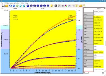
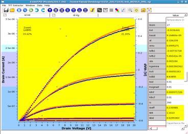
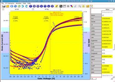
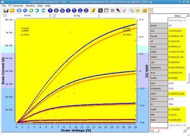
8 TFT SPICE Modeling Data preparation for SPICE model generation Cgs-Vgs Target trend vs. W/L/T 8
9 TFT Device Target Device Target (or KOP, Key Output) Target Vth SS Ion Ion2 Ioff Definition Vds=0.1V Id1=10nA*W/L Id2=1nA*W/L Vds=0.1V Vds=0.1V SS=(Vg1 - Vg2) / (log Id1 log Id2) Ids@Vgs=30V Vds=40V Ids@Vgs=30V, Vds=0.1V Ids@Vgs=-30V, Vds=40V W L T Vth Ion 9
10 Point Model Traditionally, GOA is separated from the TFT matrix. The mobility of A-Si TFT is too low for GOA. GOA is provided by an IC design company. As the number of TFT devices in a pixel cell is small, we can afford the luxury to develop point model: one SPICE model for one TFT device. The model extraction work is easy, accurate, and not a big task. When LTPS TFT is introduced, the driving capability has been much improved. The integration of GOA with TFT matrix is becoming feasible. The benefits Lower cost, smaller frame, more reliable The challenge More model cards need to be developed with more geometries A scalable model should be developed for multiple geometries 10
11 Global Model Two ways to develop a scalable model Global model Bin model Global model Measure data for a group of devices with a combination of W and L The best fitting for different devices could be conflicting to each other. Some trade-off has to be made. The model equation is the foundation to develop a good global model Lmax Lmin Wmin Wmax 11
12 Bin Model Bin model Divide the big W-L space into a few small bins, one model for one bin. Measure device data for each grid point and extract its model parameters to fit one device For each bin, use the following binning equation, Peff = P0 + LP / Leff + WP / Weff + PP / (Leff * Weff), resolve the four unknowns (P0, LP, WP, and PP) with four equations from the four grid points For any device with any W/L geometry values, use the above binning equation to calculate Peff which is the model parameter for this device Lmax Bin25 Bin26 Bin27 Bin28 Bin29 Bin30 Bin19 Bin20 Bin21 Bin22 Bin23 Bin24 Bin13 Bin14 Bin15 Bin16 Bin17 Bin18 Bin7 Bin8 Bin9 Bin10 Bin11 Bin12 Lmin Bin1 Bin2 Bin3 Bin4 Bin5 Bin6 Wmin Wmax 12

13 Process Variation Process variation Device target variation caused by different machines, materials, process conditions, etc., in lot/glass/panel hierarchy 13
14 Corner Model Typical model (TT) The mean value of measurement data is defined as the typical Corner Model (FF/SS) The three sigma from the mean is defined as the upper and lower corners of the measurement data Target Vth Ion TT Mean Mean FF Mean-3*Sigma Mean+3*Sigma SS Mean+3*Sigma Mean-3*Sigma I ON Typical Corner V TH TFT.lib.lib TT.model TFT1 nmos +vt0=0.1 ute=1...endl TT.lib FF.model TFT1 nmos +vt0=0.09 ute=1.1..endl FF.lib SS.model TFT1 nmos +vt0=0.11 ute=0.9..endl SS.lib TFT.lib FF M1 D G S TFT1 +W=10u L=1u 14
15 RPI TFT Model RPI TFT Models Continuous expressions valid through all operating regimes Gate-bias dependent field-effect mobility Leakage current in deep subthreshold: grain boundary trap states and DIBL Threshold voltage model that includes scaling with channel length and DIBL effect Temperature dependence of model parameters Kink effect caused by Vth decrease at high Vds For both a-si and poly-si Where TFT model can be improved Leakage current Subthreshold region Temperature model Stress and hysteresis effects 15

16 Leakage Current Three major mechanisms for TFT leakage current Front channel conduction: Conduction leakage current by accumulated negative carriers in front channel. Covered by RPI model. Back channel conduction: More negative gate voltage will decrease TFT band bending and the accumulated negative carriers at the front channel interface move to the back channel interface. They form the conduction leakage current in back channel I bc ~ IBCF exp[f(v GS, V DS )] Front channel emission: Higher negative gate voltage will increase the emission of carriers from the trap states in the front channel interface by virtue of Poole-Frenkel effect, and will consequently increase the leakage current I fc ~ IFCF exp(f(v DS )) exp(f V GS ) RPI Model Source Drain Front leakage Back leakage Gate Poly-Si Gate Insulator Glass Substrate 16
 DIBL & SS")
17 Subthreshold Model Improve Vds dependency Additional 2 nd order effect, the overall DIBL coefficient ~ dibl0 + f dibld, V DS Additional bias-dependent subthreshold swing calculation ~ e f(ss,v DS) DIBL & SS 17

18 Temperature Dependency T=-15 T=27 T=60 T=90 18

19 Stress Effect 19

20 Hysteresis Effect When the forward gate-voltage sweep applies on TFT device, as the V GS voltage continues to increase, the stress effect will take place as explained in the previous slide. Vice versa, when the device operates in the reverse gate-voltage sweep, V GS voltage gradually changes from ON-state to OFF-state, the carrier detrapping process will give the threshold voltage chance to recover. As the speed of de-trapping is much slower than the speed of trapping, we will see the following Hysteresis effect. 20


21 Circuit Stress Simulation Vth shift after pulsed signal stress 2-periods several periods after long time Input Signal 21


22 Circuit Stress Simulation Stress effect model used by compensation circuit design VGwhite White VGgray Gray Gray VGblack Black Id Time White Useless simulation If model has no hysteresis effect Gray Gray Id 0 Current drop due to Vth increase White Gray Very useful for compensation ckt design if model has hysteresis effect. Gray Time Black Black Current mis-match Time Time 22
23 OLED Structure OLED layers EIL/HIL: electrons and hole injection layers ETL/HTL: electrons and hole transport layers HBL/EBL: hole and electron block layers EL: emission layer OLED operation mechanism Electrons and holes are injected from EIL/HIL Electrons and holes accelerate in ETL/HTL Minority hole and electron are blocked in HBL/EBL Majority electrons/holes exciton formation and light generation in EL Cathode (Ag) EIL (Electron Injection Layer) ETL (Electron Transport Layer) HBL (Hole Blocking Layer) EL (Emissive Layer) EBL (Electron Blocking Layer) HTL (Hole Transport Layer) HIL (Hole Injection Layer) Anode (ITO) Glass 23

24 OLED I-V Model 24

25 OLED C-V Model A PWL (Piece-Wise Linear) model can be used to accurately model OLED C-V characteristics. More studies are needed to develop a more physics-based model for OLED with multiple organic layers. 25
26 OLED FPD Design Flow Full Panel Analysis IR Drop/Crosstalk/Leakage Design Entry Full Panel SPICE Simulation Pixel/GOA SPICE Simulation Panel RC Extraction Pixel/GOA Layout Design Panel Layout Verification Pixel/GOA RC Extraction Panel Layout Design 26

27 Schematic Design Entry Most important feature Approximate arbitrary shape of panel schematic, such as watch, automobile dash board, etc. 27


28 Layout Editor Most important features Support arbitrary geometric shapes Support advanced routing functions Equal Resistive Routing (ERR) Routing for a specified resistance value Routing by Aperture in given area to assure enough light transmittance Support narrow frame design Pixel placement near outline Ladder placement for GOA & DeMux ERR Narrow frame fanout attaching to outline 28


29 Layout Verification Most important features Avoid false DRC violations for arbitrary geometric shapes Avoid wrong LVS netlist generation for arbitrary geometric shapes GOA rotation at round corner GOA 29
30 False DRC Violation After rotation, the angles between a and c, and a and e may not equal to 90 degrees any more after the vertexes snapped to grid points. DRC may report a - c and d e minimum space violation which is a false alarm. 30
31 Wrong LVS MOSFET Extraction After rotation, and after the vertexes snapped to grid points, MOSFET extraction could be wrong as the S-pin and D-pin may not touch the gate area. 31


32 RC Extraction Most important features High accuracy, high performance, 3D RC extraction. Pixel 3D RC extraction. High accuracy is required. Metal mesh replaced metal solid piece for flexible touch panel. Thousands of grid points for 3D coupling capacitor extraction between the finger and the metal mesh. Accurate and Fast 3D RC Extraction Coupling C Extraction for Flexible Touch Panel 32

33 OLED Full Panel Simulation OLED is a current driving device. FastSpice is not accurate for current simulation. Traditional SPICE is not able to handle the size of a full panel circuit. E.g., a 4K OLED TV has 3840*2160*8*3 (7T1C pixel) =200M TFT/OLED devices, plus 10x more parasitic RC elements. VDD/VSS IR drop and leakage current are the most critical concern for OLED FPD design. Full panel simulation is the only way to verify any issues in advance. 33

34 OLED Full Panel Simulation White: 96(1920/20)x540(1080/2) (1/40) Red: 96(1920/20)x1080 (1/20) Green: 192(1920/10)x1080 (1/10) A partial circuit may not be able to represent the full panel circuit. Full panel simulation considers IRdrop, leakage, etc. 34

35 Full Panel IR Drop Analysis Must have for OLED FPD as high accuracy of OLED current is needed Simulates voltage distribution for power and ground nets in full panel Extract accurate but efficient resistive network PAD1 PAD2 RPIL RPIR P0 P0_0 PR_1_1 PG_1_1 PB_1_1 PR_2_1 PG_2_1 PB_2_1 P7_0 P3 RPH RPH RPH RPH RPH RPH RPH RPH RPH RPV RPS RPS RPS RPS RPS RPS RPV P0_1 R_1_1 G_1_1 B_1_1 R_2_1 G_2_1 B_2_1 P7_1 RPS RVH RVH RVH RVH RVH RPS RPL RPV RVV RVV RVV RVV RVV RVV RPV RPR P0_2 R_1_2 G_1_2 B_1_2 R_2_2 G_2_2 B_2_2 P7_2 RPS RVH RVH RVH RVH RVH RPS RPV RPS RPS RPS RPS RPS RPS RPV P1 P0_3 PR_1_2 PG_1_2 PB_1_2 PR_2_2 PG_2_2 PB_2_2 P7_3 P2 RPH RPH RPH RPH RPH RPH RPH RPH RPH 35
36 Future Work SPICE Modeling OLED C-V model development OLED stress model development Statistical model generation with small sampling size Circuit Simulation Hardware acceleration to speed up full panel simulation for 4K (200M TFT/OLED elements) and 8K (800M TFT/OLED elements) OLED Circuit stress simulation Design Verification Handle arbitrary shapes more efficiently 36
37 Thank You! 37
Overview of All Pixel Circuits for Active Matrix Organic Light Emitting Diode (AMOLED)
") Chapter 2 Overview of All Pixel Circuits for Active Matrix Organic Light Emitting Diode (AMOLED) ---------------------------------------------------------------------------------------------------------------
Chapter 2 Overview of All Pixel Circuits for Active Matrix Organic Light Emitting Diode (AMOLED) ---------------------------------------------------------------------------------------------------------------
 Chapter 3 Evaluated Results of Conventional Pixel Circuit, Other Compensation Circuits and Proposed Pixel Circuits for Active Matrix Organic Light Emitting Diodes (AMOLEDs) -------------------------------------------------------------------------------------------------------
Design of Organic TFT Pixel Electrode Circuit for Active-Matrix OLED Displays
 JOURNAL OF COMPUTERS, VOL. 3, NO. 3, MARCH 2008 1 Design of Organic TFT Pixel Electrode Circuit for Active-Matrix Displays Aram Shin, Sang Jun Hwang, Seung Woo Yu, and Man Young Sung 1) Semiconductor and
COMPENSATION FOR THRESHOLD INSTABILITY OF THIN-FILM TRANSISTORS
 COMPENSATION FOR THRESHOLD INSTABILITY OF THIN-FILM TRANSISTORS by Roberto W. Flores A Thesis Submitted to the Graduate Faculty of George Mason University in Partial Fulfillment of The Requirements for
 Chapter 1 Introduction --------------------------------------------------------------------------------------------------------------- 1.1 Overview of the Organic Light Emitting Diode (OLED) Displays Flat
P_02_1011:A Novel Pixel Circuit to Compensate for the Degradation of OLED Luminance in High-Resolution AMOLED Displays
 P_0_1011:A Novel Pixel Circuit to Compensate for the Degradation of OLED Luminance in High-Resolution AMOLED Displays National Cheng Kung University Department of Electrical Engineering IDBA Lab. Advisor..
Phosphorescent OLED Technologies: The Next Wave. Plastic Electronics Conference Oct 9, 2012
 Phosphorescent OLED Technologies: The Next Wave Plastic Electronics Conference Oct 9, 2012 UDC Company Focus IP innovator, technology developer, patent licensor and materials supplier for the rapidly growing
VARIOUS DISPLAY TECHNOLOGIESS
 VARIOUS DISPLAY TECHNOLOGIESS Mr. Virat C. Gandhi 1 1 Computer Department, C. U. Shah Technical Institute of Diploma Studies Abstract A lot has been invented from the past till now in regards with the
Comparative Analysis of Organic Thin Film Transistor Structures for Flexible E-Paper and AMOLED Displays
 Comparative Analysis of Organic Thin Film Transistor Structures for Flexible E-Paper and AMOLED Displays Linrun Feng, Xiaoli Xu and Xiaojun Guo ECS Trans. 2011, Volume 37, Issue 1, Pages 105-112. doi:
Monolithic CMOS Power Supply for OLED Display Driver / Controller IC
 Monolithic CMOS Power Supply for OLED Display Driver / Controller IC Cheung Fai Lee SOLOMON Systech Limited Abstract This paper presents design considerations of a power supply IC to meet requirements
Liquid Crystal Display (LCD)
") Liquid Crystal Display (LCD) When coming into contact with grooved surface in a fixed direction, liquid crystal molecules line up parallelly along the grooves. When coming into contact with grooved surface
Liquid Crystal Display (LCD) When coming into contact with grooved surface in a fixed direction, liquid crystal molecules line up parallelly along the grooves. When coming into contact with grooved surface
Performance Comparison of Bilayer and Multilayer OLED
 Performance Comparison of Bilayer and Multilayer OLED Akanksha Uniyal, Poornima Mittal * Department of Electronics and Communication School of Engineering and Technology Graphic Era University, Dehradun-248002,
FLEX2017 June, Monterey, USA Dr Mike Cowin, CMO, SmartKem.
 FLEX2017 June, Monterey, USA Dr Mike Cowin, CMO, SmartKem. FLEX2017 June, Monterey, USA Dr Mike Cowin, CMO, SmartKem. EU H2020 FLEXTRANs Grant Objectives A 24 month project (started September 2016) (Grant
1. Publishable summary
 1. Publishable summary 1.1. Project objectives. The target of the project is to develop a highly reliable high brightness conformable low cost scalable display for demanding applications such as their
[1.9] AMOLED 공정 Introduction OLED Materials Patterning Process Process Equipments
![[1.9] AMOLED 공정 Introduction OLED Materials Patterning Process Process Equipments](/thumbs/73/69073032.jpg "[1.9] AMOLED 공정 Introduction OLED Materials Patterning Process Process Equipments") [1.9] AMOLED 공정 1.9.1. Introduction 1.9.2. OLED Materials 1.9.3. Patterning Process 1.9.4. Process Equipments OLED : Organic Light Emitting Diode Organic EL : Organic Electroluminescent 재료및공정 재료의발광메카니즘
[1.9] AMOLED 공정 1.9.1. Introduction 1.9.2. OLED Materials 1.9.3. Patterning Process 1.9.4. Process Equipments OLED : Organic Light Emitting Diode Organic EL : Organic Electroluminescent 재료및공정 재료의발광메카니즘
Sep 09, APPLICATION NOTE 1193 Electronic Displays Comparison
 Sep 09, 2002 APPLICATION NOTE 1193 Electronic s Comparison Abstract: This note compares advantages and disadvantages of Cathode Ray Tubes, Electro-Luminescent, Flip- Dot, Incandescent Light Bulbs, Liquid
AMOLED Manufacturing Process Report SAMPLE
 AMOLED Manufacturing Process Report SAMPLE 2018 AMOLED Manufacturing Process Report The report analyzes the structure and manufacturing process by dividing AMOLED into small & medium-sized rigid OLED,
Silole Derivative Properties in Organic Light Emitting Diodes
 Silole Derivative Properties in Organic Light Emitting Diodes E. Duncan MLK HS Physics Teacher Mentors: Prof. Bernard Kippelen & Dr. Benoit Domercq Introduction Theory Methodology Results Conclusion Acknowledgements
(12) Patent Application Publication (10) Pub. No.: US 2005/ A1
 Patent Application Publication (10) Pub. No.: US 2005/ A1") (19) United States US 2005O285825A1 (12) Patent Application Publication (10) Pub. No.: US 2005/0285825A1 E0m et al. (43) Pub. Date: Dec. 29, 2005 (54) LIGHT EMITTING DISPLAY AND DRIVING (52) U.S. Cl....
(19) United States US 2005O285825A1 (12) Patent Application Publication (10) Pub. No.: US 2005/0285825A1 E0m et al. (43) Pub. Date: Dec. 29, 2005 (54) LIGHT EMITTING DISPLAY AND DRIVING (52) U.S. Cl....
UniMCO 4.0: A Unique CAD Tool for LED, OLED, RCLED, VCSEL, & Optical Coatings
 UniMCO 4.0: A Unique CAD Tool for LED, OLED, RCLED, VCSEL, & Optical Coatings 1 Outline Physics of LED & OLED Microcavity LED (RCLED) and OLED (MCOLED) UniMCO 4.0: Unique CAD tool for LED-Based Devices
Development of OLED Lighting Applications Using Phosphorescent Emission System
 Development of OLED Lighting Applications Using Phosphorescent Emission System Kazuhiro Oikawa R&D Department OLED Lighting Business Center KONICA MINOLTA ADVANCED LAYERS, INC. October 10, 2012 Outline
AMOLED compensation circuit patent analysis
 IHS Electronics & Media Key Patent Report AMOLED compensation circuit patent analysis AMOLED pixel driving circuit with threshold voltage and IR-drop compensation July 2013 ihs.com Ian Lim, Senior Analyst,
Scalable self-aligned active matrix IGZO TFT backplane technology and its use in flexible semi-transparent image sensors. Albert van Breemen
 Scalable self-aligned active matrix IGZO TFT backplane technology and its use in flexible semi-transparent image sensors Albert van Breemen Image sensors today 1 Dominated by silicon based technology on
Liquid Crystal Displays
 Liquid Crystal Displays Cosmin Ioniţă - Spring 2006 - A brief history 1888 - Friedrich Reinitzer, an Austrian chemist working in the Institute of Plant Physiology at the University of Prague, discovered
New Pixel Circuit Compensating Poly-si TFT Threshold-voltage Shift for a Driving AMOLED
 Journal of the Korean Physical Society, Vol. 56, No. 4, April 2010, pp. 1185 1189 New Pixel Circuit Compensating Poly-si TFT Threshold-voltage Shift for a Driving AMOLED C. L. Fan, Y. Y. Lin, B. S. Lin
Joint Development of Ultra-Bright, Inorganic EL Light-Emitting Materials. November 2, 2005 KURARAY CO., LTD.
 Joint Development of Ultra-Bright, Inorganic EL Light-Emitting Materials November 2, 2005 KURARAY CO., LTD. Sales Trends of Display-related Products (Kuraray (standalone)) FY1994 FY1999 FY2004 Sales Ratio
Solution Processable OLEDs. Anna Hayer EuroDisplay /09/2013
 Solution Processable LEDs Merck KGaA Anna Hayer EuroDisplay 2013 Content 1 Introduction 2 LED Basics 3 Challenges for Solution Processing 4 Current Results 5 Summary 2 EuroDisplay 2013 Hayer - Merck Solution
Next Generation of Poly-Si TFT Technology: Material Improvements and Novel Device Architectures for System-On-Panel (SOP)
") Next Generation of Poly-Si TFT Technology: Material Improvements and Novel Device Architectures for System-On-Panel (SOP) Tolis Voutsas* Paul Schuele* Bert Crowder* Pooran Joshi* Robert Sposili* Hidayat
Next Generation of Poly-Si TFT Technology: Material Improvements and Novel Device Architectures for System-On-Panel (SOP) Tolis Voutsas* Paul Schuele* Bert Crowder* Pooran Joshi* Robert Sposili* Hidayat
TipatOr. Liquid metal switch (LMS) display technology. Avi Fogel
 display technology. Avi Fogel") TipatOr Liquid metal switch (LMS) display technology Avi Fogel 972-52-5702938 avifog@gmail.com Who is behind TipatOr TipatOr emerged from a merger of 2 expert groups in the fields of MEMS and Displays
TipatOr Liquid metal switch (LMS) display technology Avi Fogel 972-52-5702938 avifog@gmail.com Who is behind TipatOr TipatOr emerged from a merger of 2 expert groups in the fields of MEMS and Displays
FinFETs & SRAM Design
 FinFETs & SRAM Design Raymond Leung VP Engineering, Embedded Memories April 19, 2013 Synopsys 2013 1 Agenda FinFET the Device SRAM Design with FinFETs Reliability in FinFETs Summary Synopsys 2013 2 How
Displays and framebuffers
 Reading Optional Displays and framebuffers Brian Curless CSE 557 Autumn 2017 OpenGL Programming Guide (the red book available online): First four sections of chapter 2 First section of chapter 6 Foley
An Overview of OLED Display Technology
 page:1 An Overview of OLED Display Technology Homer Antoniadis OSRAM Opto Semiconductors Inc. San Jose, CA page:2 Outline! OLED device structure and operation! OLED materials (polymers and small molecules)!
OLED Status quo and our position
 OLED Status quo and our position Information Day 2013 A Deep Dive into the LC&OLED Business Dr. Udo Heider Vice President OLED Darmstadt, Germany June 26, 2013 Disclaimer Remarks All comparative figures
P-224: Damage-Free Cathode Coating Process for OLEDs
 P-224: Damage-Free Cathode Coating Process for OLEDs Shiva Prakash DuPont Displays, 6 Ward Drive, Santa Barbara, CA 937, USA Abstract OLED displays require the growth of inorganic films over organic films.
A novel TFT-OLED integration for OLED-independent pixel programming in amorphous-si AMOLED pixels
 A novel TFT-OLED integration for OLED-independent pixel programming in amorphous-si AMOLED pixels Bahman Hekmatshoar Alex Z. Kattamis Kunigunde Cherenack Sigurd Wagner James C. Sturm Abstract The direct
Organic Light Emitting Diodes
 ISSN: 2278 0211 (Online) Organic Light Emitting Diodes Badisa Sai Ram Krsihna Final Year B.Tech, Dept. of ECE, KL University, Vaddeswaram, AP, India Angadi Suresh Associate Professor B.Tech, Dept. of ECE,
(12) Patent Application Publication (10) Pub. No.: US 2003/ A1
 Patent Application Publication (10) Pub. No.: US 2003/ A1") (19) United States US 2003.01.07565A1 (12) Patent Application Publication (10) Pub. No.: US 2003/0107565A1 Libsch et al. (43) Pub. Date: Jun. 12, 2003 (54) ACTIVE MATRIX OLED VOLTAGE DRIVE PXEL CIRCUIT
(19) United States US 2003.01.07565A1 (12) Patent Application Publication (10) Pub. No.: US 2003/0107565A1 Libsch et al. (43) Pub. Date: Jun. 12, 2003 (54) ACTIVE MATRIX OLED VOLTAGE DRIVE PXEL CIRCUIT
LCD MODULE SPECIFICATION
 TECHNOLOGY CO., LTD. LCD MODULE SPECIFICATION Model : MI0220IT-1 Revision Engineering Date Our Reference DOCUMENT REVISION HISTORY DOCUMENT REVISION DATE DESCRIPTION FROM TO A 2008.03.10 First Release.
Requirement for graphic arts display
 Requirement for graphic arts display Content Development Division of National Digital Archives Program, Taiwan Date: 95/12/5 中島賢人 : Masato Nakashima Product Manager, Graphic Solutions Overseas Sales &
(12) United States Patent
 United States Patent") USOO7023408B2 (12) United States Patent Chen et al. (10) Patent No.: (45) Date of Patent: US 7,023.408 B2 Apr. 4, 2006 (54) (75) (73) (*) (21) (22) (65) (30) Foreign Application Priority Data Mar. 21,
USOO7023408B2 (12) United States Patent Chen et al. (10) Patent No.: (45) Date of Patent: US 7,023.408 B2 Apr. 4, 2006 (54) (75) (73) (*) (21) (22) (65) (30) Foreign Application Priority Data Mar. 21,
The Company. A leading OLED player
 The Company A leading OLED player Novaled is the company to trade with, work for and invest in. Our company focuses on proprietary organic materials and complementary innovative technologies for superior
Data Supply Voltage Reduction Scheme for Low-Power AMOLED Displays
 Data Supply Voltage Reduction Sche for Low-Power AMOLED Displays Hyoungsik Nam and Hoon Jeong This paper donstrates a new driving sche that allows reducing the supply voltage of data drivers for lowpower
High-resolution screens have become a mainstay on modern smartphones. Initial. Displays 3.1 LCD
 3 Displays Figure 3.1. The University of Texas at Austin s Stallion Tiled Display, made up of 75 Dell 3007WPF LCDs with a total resolution of 307 megapixels (38400 8000 pixels) High-resolution screens
Technology White Paper Plasma Displays. NEC Technologies Visual Systems Division
 Technology White Paper Plasma Displays NEC Technologies Visual Systems Division May 1998 1 What is a Color Plasma Display Panel? The term Plasma refers to a flat panel display technology that utilizes
CHAPTER 9. Actives Devices: Diodes, Transistors,Tubes
 CHAPTER 9 Actives Devices: Diodes, Transistors,Tubes 1 The electrodes of a semiconductor diode are known as anode and cathode. In a semiconductor diode, electrons flow from cathode to anode. In order for
Design and Simulation of High Power RF Modulated Triode Electron Gun. A. Poursaleh
 Design and Simulation of High Power RF Modulated Triode Electron Gun A. Poursaleh National Academy of Sciences of Armenia, Institute of Radio Physics & Electronics, Yerevan, Armenia poursaleh83@yahoo.com
Basically we are fooling our brains into seeing still images at a fast enough rate so that we think its a moving image.
 Basically we are fooling our brains into seeing still images at a fast enough rate so that we think its a moving image. The formal definition of a Moving Picture... A sequence of consecutive photographic
EL302 DIGITAL INTEGRATED CIRCUITS LAB #3 CMOS EDGE TRIGGERED D FLIP-FLOP. Due İLKER KALYONCU, 10043
 EL302 DIGITAL INTEGRATED CIRCUITS LAB #3 CMOS EDGE TRIGGERED D FLIP-FLOP Due 16.05. İLKER KALYONCU, 10043 1. INTRODUCTION: In this project we are going to design a CMOS positive edge triggered master-slave
ID C10C: Flat Panel Display Basics
 ID C10C: Flat Panel Display Basics Renesas Electronics America Inc. Robert Dunhouse, Display BU Engineering Manager 12 October 2010 Revision 1.1 Robert F. Dunhouse, Jr. Displays Applications Engineering
Report on 4-bit Counter design Report- 1, 2. Report on D- Flipflop. Course project for ECE533
 Report on 4-bit Counter design Report- 1, 2. Report on D- Flipflop Course project for ECE533 I. Objective: REPORT-I The objective of this project is to design a 4-bit counter and implement it into a chip
In-Cell Projected Capacitive Touch Panel Technology
 1384 INVITED PAPER Special Section on Electronic Displays In-Cell Projected Capacitive Touch Panel Technology Yasuhiro SUGITA a), Member, Kazutoshi KIDA, and Shinji YAMAGISHI, Nonmembers SUMMARY We describe
AM-OLED pixel circuits suitable for TFT array testing. Research Division Almaden - Austin - Beijing - Haifa - India - T. J. Watson - Tokyo - Zurich
 RT0565 Engineering Technology 4 pages Research Report February 3, 2004 AM-OLED pixel circuits suitable for TFT array testing Y. Sakaguchi, D. Nakano IBM Research, Tokyo Research Laboratory IBM Japan, Ltd.
Display Systems. Viewing Images Rochester Institute of Technology
 Display Systems Viewing Images 1999 Rochester Institute of Technology In This Section... We will explore how display systems work. Cathode Ray Tube Television Computer Monitor Flat Panel Display Liquid
Flat Panel Displays: LCD Technologies and Trends
 Flat Panel Displays: LCD Technologies and Trends Robert Dunhouse, Sr. Engineering Manager, Display BU Class ID: 4C01B Renesas Electronics America Inc. Robert F. Dunhouse, Jr. Sr. Engineering Manager, Display
ELEC 4609 IC DESIGN TERM PROJECT: DYNAMIC PRSG v1.2
 ELEC 4609 IC DESIGN TERM PROJECT: DYNAMIC PRSG v1.2 The goal of this project is to design a chip that could control a bicycle taillight to produce an apparently random flash sequence. The chip should operate
ORGANIC light-emitting diode (OLED) displays are
 displays are") 100 IEEE/OSA JOURNAL OF DISPLAY TECHNOLOGY, VOL. 1, NO. 1, SEPTEMBER 2005 A New Pixel Circuit for Driving Organic Light-Emitting Diode With Low Temperature Polycrystalline Silicon Thin-Film Transistors
100 IEEE/OSA JOURNAL OF DISPLAY TECHNOLOGY, VOL. 1, NO. 1, SEPTEMBER 2005 A New Pixel Circuit for Driving Organic Light-Emitting Diode With Low Temperature Polycrystalline Silicon Thin-Film Transistors
8.1: Advancements and Outlook of High Performance Active-Matrix OLED Displays
 8.1: Advancements and Outlook of High Performance Active-Matrix OLED Displays Takatoshi Tsujimura *, Wei Zhu, Seiichi Mizukoshi, Nobuyuki Mori, Koichi Miwa, Shinya Ono, Yuichi Maekawa, Kazuyoshi Kawabe,
the Most Popular Display Technology?
 Why is LCD the Most Popular Display Technology? History of Liquid Crystal Display (LCD) As early as 1889, scientists discovered that chemicals such as cholesteryl benzoate, when melted into liquid form,
DESIGN AND OPTIMIZATION OF LARGE-AREA OLEDS
 DESIGN AND OPTIMIZATION OF LARGE-AREA OLEDS BY ELECTRO-THERMAL MODELING S. Altazin 1, R. Hiestand 1, C. Kirsch 2, M. Diethelm 1,2, L. Penninck 1, M. A. Maindin 1, M. Fontenlos 1, B. Ruhstaller 1,2* beat.ruhstaller@zhaw.ch
(12) United States Patent (10) Patent No.: US 6,885,157 B1
 United States Patent (10) Patent No.: US 6,885,157 B1") USOO688.5157B1 (12) United States Patent (10) Patent No.: Cok et al. (45) Date of Patent: Apr. 26, 2005 (54) INTEGRATED TOUCH SCREEN AND OLED 6,504,530 B1 1/2003 Wilson et al.... 345/173 FLAT-PANEL DISPLAY
USOO688.5157B1 (12) United States Patent (10) Patent No.: Cok et al. (45) Date of Patent: Apr. 26, 2005 (54) INTEGRATED TOUCH SCREEN AND OLED 6,504,530 B1 1/2003 Wilson et al.... 345/173 FLAT-PANEL DISPLAY
Nanostructured super-period gratings and photonic crystals for enhancing light extraction efficiency in OLEDs
 Final Project Report E3390 Electronic Circuits Design Lab Nanostructured super-period gratings and photonic crystals for enhancing light extraction efficiency in OLEDs Padmavati Sridhar Submitted in partial
LM16X21A Dot Matrix LCD Unit
 LCD Data Sheet FEATURES STC (Super Twisted igh Contrast) Yellow Green Transmissive Type Low Power Consumption Thin, Lightweight Design Permits Easy Installation in a Variety of Equipment General Purpose
Lecture Flat Panel Display Devices
 Lecture 13 6.111 Flat Panel Display Devices Outline Overview Flat Panel Display Devices How do Displays Work? Emissive Displays Light Valve Displays Display Drivers Addressing Schemes Display Timing Generator
Advances in AMOLED Technologies
 14 Advances in AMOLED Technologies Y.-M. Alan Tsai, James Chang, D.Z. Peng, Vincent Tseng, Alex Lin, L.J. Chen, and Poyen Lu TPO Displays Corp., Chunan, Taiwan 14.1 Introduction In all electronic displays,
Stacked OLEDs for Lighting Applications - Improvement of the yellow building block
 Stacked OLEDs for Lighting Applications Improvement of the yellow building block 13/12/2010 Carola Diez Osram Opto Semiconductors GmbH and University of Augsburg OLED Lighting White organic light emitting
Lecture Flat Panel Display Devices
 Lecture 1 6.976 Flat Panel Display Devices Outline Overview of 6.976 Overview Flat Panel Display Devices Course website http://hackman.mit.edu Reading Assignment: Article by Alt and Noda, IBM Journal of
Flexible Electronics Production Deployment on FPD Standards: Plastic Displays & Integrated Circuits. Stanislav Loboda R&D engineer
 Flexible Electronics Production Deployment on FPD Standards: Plastic Displays & Integrated Circuits Stanislav Loboda R&D engineer The world-first small-volume contract manufacturing for plastic TFT-arrays
Analog Circuits Prof. Nagendra Krishnapura Department of Electrical Engineering Indian Institute of Technology, Madras. Module - 04 Lecture 12
 Analog Circuits Prof. Nagendra Krishnapura Department of Electrical Engineering Indian Institute of Technology, Madras Module - 04 Lecture 12 So, far we have discussed common source amplifier using an
(12) United States Patent
 United States Patent") (12) United States Patent Sanford et al. USOO6734636B2 (10) Patent No.: (45) Date of Patent: May 11, 2004 (54) OLED CURRENT DRIVE PIXEL CIRCUIT (75) Inventors: James Lawrence Sanford, Hopewell Junction,
(12) United States Patent Sanford et al. USOO6734636B2 (10) Patent No.: (45) Date of Patent: May 11, 2004 (54) OLED CURRENT DRIVE PIXEL CIRCUIT (75) Inventors: James Lawrence Sanford, Hopewell Junction,
High ResolutionCross Strip Anodes for Photon Counting detectors
 High ResolutionCross Strip Anodes for Photon Counting detectors Oswald H.W. Siegmund, Anton S. Tremsin, Robert Abiad, J. Hull and John V. Vallerga Space Sciences Laboratory University of California Berkeley,
Digital time-modulation pixel memory circuit in LTPS technology
 Digital time-modulation pixel memory circuit in LTPS technology Szu-Han Chen Ming-Dou Ker Tzu-Ming Wang Abstract A digital time-modulation pixel memory circuit on glass substrate has been designed and
PROCESS TECHNOLOGIES FOR ADVANCED ORGANIC ELECTRONIC DEVICES: MICRODISPLAYS, LIGHTING AND SOLAR CELLS
 PROCESS TECHNOLOGIES FOR ADVANCED ORGANIC ELECTRONIC DEVICES: MICRODISPLAYS, LIGHTING AND SOLAR CELLS Dr. Christian May Fraunhofer IPMS - Center for Organic Materials and Electronic Devices Dresden COMEDD
Display Devices & its Interfacing
 Display Devices & its Interfacing 3 Display systems are available in various technologies such as i) Cathode ray tubes (CRTs), ii) Liquid crystal displays (LCDs), iii) Plasma displays, and iv) Light emitting
These are used for producing a narrow and sharply focus beam of electrons.
 CATHOD RAY TUBE (CRT) A CRT is an electronic tube designed to display electrical data. The basic CRT consists of four major components. 1. Electron Gun 2. Focussing & Accelerating Anodes 3. Horizontal
Modifying the Scan Chains in Sequential Circuit to Reduce Leakage Current
 IOSR Journal of VLSI and Signal Processing (IOSR-JVSP) Volume 3, Issue 1 (Sep. Oct. 2013), PP 01-09 e-issn: 2319 4200, p-issn No. : 2319 4197 Modifying the Scan Chains in Sequential Circuit to Reduce Leakage
International Research Journal of Engineering and Technology (IRJET) e-issn: Volume: 03 Issue: 07 July p-issn:
 e-issn: Volume: 03 Issue: 07 July p-issn:") IC Layout Design of Decoder Using Electrical VLSI System Design 1.UPENDRA CHARY CHOKKELLA Assistant Professor Electronics & Communication Department, Guru Nanak Institute Of Technology-Ibrahimpatnam (TS)-India
IC Layout Design of Decoder Using Electrical VLSI System Design 1.UPENDRA CHARY CHOKKELLA Assistant Professor Electronics & Communication Department, Guru Nanak Institute Of Technology-Ibrahimpatnam (TS)-India
HEBS: Histogram Equalization for Backlight Scaling
 HEBS: Histogram Equalization for Backlight Scaling Ali Iranli, Hanif Fatemi, Massoud Pedram University of Southern California Los Angeles CA March 2005 Motivation 10% 1% 11% 12% 12% 12% 6% 35% 1% 3% 16%
A NOVEL METHOD FOR TESTING LCD BY INTEGRATING SHORTING BAR AND TAGUCHI DOE TECHNOLOGIES
 This article has been peer reviewed and accepted for publication in JMST but has not yet been copyediting, typesetting, pagination and proofreading process. Please note that the publication version of
Advancement in the Technology of Organic Light Emitting Diodes
 IOSR Journal of Electrical and Electronics Engineering (IOSR-JEEE) e-issn: 2278-1676,p-ISSN: 2320-3331, PP 06-10 www.iosrjournals.org Advancement in the Technology of Organic Light Emitting Diodes Rohan
High Efficiency White OLEDs for Lighting
 CIE-y Journal of Photopolymer Science and Technology Volume 25, Number 3 (2012) 321 326 2012CPST High Efficiency White OLEDs for Lighting Takuya Komoda, Kazuyuki Yamae, Varutt Kittichungchit, Hiroya Tsuji
VLSI Chip Design Project TSEK06
 VLSI Chip Design Project TSEK06 Project Description and Requirement Specification Version 1.1 Project: High Speed Serial Link Transceiver Project number: 4 Project Group: Name Project members Telephone
Display Technologies CMSC 435. Slides based on Dr. Luebke s slides
 Display Technologies CMSC 435 Slides based on Dr. Luebke s slides Recap: Transforms Basic 2D Transforms: Scaling, Shearing, Rotation, Reflection, Composition of 2D Transforms Basic 3D Transforms: Rotation,
Flat Panel Displays: 1. Introduction
 OSE-6820 Flat Panel Displays: 1. Introduction Prof. Shin-Tson Wu College of Optics & Photonics University of Central Florida Email: swu@mail.ucf.edu Office: CREOL 280 Phone: 407-823-4763 UCF College of
Interactive Virtual Laboratories for Studying OLED Technology
 Interactive Virtual Laboratories for Studying OLED Technology Phillip I. Cherner 1 Abstract The paper describes a virtual OLED laboratory designed to introduce young people to one of the most contemporary
Boolean, 1s and 0s stuff: synthesis, verification, representation This is what happens in the front end of the ASIC design process
 (Lec 11) From Logic To Layout What you know... Boolean, 1s and 0s stuff: synthesis, verification, representation This is what happens in the front end of the ASIC design process High-level design description
Organic light emitting diodes for display technology
 Organic light emitting diodes for display technology Shamna Shamsudeen MScTI - ZITI-Heidelberg University OLED ZITI, Uni Heidelberg Page1 What s Light Light: Visible part of EM spectra. Ref:[1] Thermoluminescence:
Compact Size Perfect for rack mount router and other applications with space limitations.
 Wide View Compact LCD 6 x Pushbutton DISTINCTIVE CHARACTERISTICS Compact Size Perfect for rack mount router and other applications with space limitations. Compact body size: 19.0mm (.78 ) x 18.0mm (.709
ISO/TR TECHNICAL REPORT. Ergonomics of human-system interaction Part 309: Organic light-emitting diode (OLED) displays
 displays") TECHNICAL REPORT ISO/TR 9241-309 First edition 2008-11-15 Ergonomics of human-system interaction Part 309: Organic light-emitting diode (OLED) displays Ergonomie de l'interaction homme-système Partie 309:
TECHNICAL REPORT ISO/TR 9241-309 First edition 2008-11-15 Ergonomics of human-system interaction Part 309: Organic light-emitting diode (OLED) displays Ergonomie de l'interaction homme-système Partie 309:
LEDs, New Light Sources for Display Backlighting Application Note
 LEDs, New Light Sources for Display Backlighting Application Note Introduction Because of their low intensity, the use of light emitting diodes (LEDs) as a light source for backlighting was previously
SXGA096 DESIGN REFERENCE BOARD
 SXGA096 DESIGN REFERENCE BOARD For Use with all emagin SXGA096 OLED Microdisplays USER S MANUAL VERSION 1.0 TABLE OF CONTENTS D01-501152-01 SXGA096 Design Reference Board User s Manual i 1. INTRODUCTION...
Application Note. Introduction of JDI MIP reflective type color LCD
 April, 2016 Application Note Introduction of JDI MIP reflective type color Introduction JDI releases a series of MIP (memory in pixel) reflective type color s which realize high reflectance performance
Technical background and design options to raise energy efficiency and reduce the environmental impact of TVs
 Appliances Guide Get super efficient appliances Technical background and design options to raise energy efficiency and reduce the environmental impact of TVs Author Thomas Götz Published 11/2015 bigee.net
Development of Simple-Matrix LCD Module for Motion Picture
 Development of Simple-Matrix LCD Module for Motion Picture Kunihiko Yamamoto* Shinya Takahashi* Kouki Taniguchi* * A1203 Project Team Abstract A simple-matrix LCD module (12.1-in. SVGA) has been developed
Abstract. Keywords INTRODUCTION. Electron beam has been increasingly used for defect inspection in IC chip
 Abstract Based on failure analysis data the estimated failure mechanism in capacitor like device structures was simulated on wafer in Front End of Line. In the study the optimal process step for electron
DEM A VMH-PW-N 5 TFT
 Display Elektronik GmbH TFT MODULE DEM 7201280A VMH-PW-N 5 TFT Product Specification Ver.: 0 25.08.2017 Revision History VERSION DATE REVISED PAGE NO. Note 0 25.08.2017 First Issue Version: 0 PAGE: 2 Contents
Solid State Devices 4B6
 Solid State Devices 4B6 Lecture 13 Projection and 3D displays: LCD, DLP and LCOS Daping Chu Lent 2016 Development of flat panel displays (FPDs) (LCD) in early days 1 A 105 inch TFT-LCD 4k2k curved panel
Display Technologies. Corning: The Technology Behind the Glass
 Display Technologies Corning: The Technology Behind the Glass Dr. David Chen Director, Application Engineering and Asia Commercial Technology Taiwan Corning Display Technologies Taiwan June 13, 2008 Forward
2.2. VIDEO DISPLAY DEVICES
 Introduction to Computer Graphics (CS602) Lecture 02 Graphics Systems 2.1. Introduction of Graphics Systems With the massive development in the field of computer graphics a broad range of graphics hardware
CAEN Tools for Discovery
 Viareggio March 28, 2011 Introduction: what is the SiPM? The Silicon PhotoMultiplier (SiPM) consists of a high density (up to ~10 3 /mm 2 ) matrix of diodes connected in parallel on a common Si substrate.
Chapter 2 Circuits and Drives for Liquid Crystal Devices
 Chapter 2 Circuits and Drives for Liquid Crystal Devices Hideaki Kawakami 2.1 Circuits and Drive Methods: Multiplexing and Matrix Addressing Technologies Hideaki Kawakami 2.1.1 Introduction The liquid