Scalable self-aligned active matrix IGZO TFT backplane technology and its use in flexible semi-transparent image sensors. Albert van Breemen
|
|
|
- Peregrine Stevens
- 5 years ago
- Views:
Transcription


1


2
3 Scalable self-aligned active matrix IGZO TFT backplane technology and its use in flexible semi-transparent image sensors Albert van Breemen


4 Image sensors today 1 Dominated by silicon based technology on rigid substrates - High performance - Large area applications difficult and/or expensive - Rigidity hampers integration in products where form factor is important - Mechanical integrity poor CMOS sensor Fingerprint sensor Digital X-ray detectors 1 Market size estimated to reach USD 17.5 Billion by 2020 CAGR of 30% between 2015 and 2020
-transparent Enable new products and product design")
5 Flexible image sensors Can offer similar performance as compared to silicon, but: - can be processed over large area and hence have a competitive cost per area ratio - are thin and light weight - are robust - are conformable - can be (semi)-transparent Enable new products and product design
6 Applications semi-transparent image sensors Stacked image sensors in cameras or lens-less color scanners RGB photodetectors Stacked image sensors Light Reduced photon shot noise Conventional image sensor with color filters Semi-transparent backplane Increased resolution T. Takagiet al. International Symposium on Electronic Imaging 2016, 264.1


7 Applications semi-transparent image sensors New user interfaces also in combination with displays - Gesture, form & shape recognition - New ways of interaction with smart walls, wearable devices or IoT nodes Security & Authentication 7


8 Our scalable technology choices O P D Thin-Film Encapsulation Transparent Transparent top electrode top electrode Bottom electrode Oxide semiconductor TFT backplane on plastic - 10x higher mobility than a-si - Ultra-low leakage currents, so higher sensitivity T F T S IGZO G PI foil D Organic photodetector frontplane - Low process temperatures, compatible with plastic substrates - Large area deposition: competitive cost per area ratio Transparent thin-film encapsulation - Developed by Holst Centre, used in products Holst Centre TFT pilot line 8
 at the anode Amorphous indium-gallium-zinc-oxide as electron transport layer in organic photodetectors H. Arora et al.")
9 Organic photodetector (OPD) Interface between the electrodes and the OPD blend layer is of prime importance in order to control the dark current Transparent top anode HTL = MoOx ETL = IGZO Cathode Interface can be modified by: - a Hole Transport Layer (HTL) at the anode Amorphous indium-gallium-zinc-oxide as electron transport layer in organic photodetectors H. Arora et al. Applied Physics Letters, 106, (2015) - an Electron Transport Layer (ETL) at the cathode Indium Gallium Zinc Oxide (IGZO) proves to be an excellent ETL in OPDs 9
10 Performance OPD J dark 3x10⁻⁸ ma/cm 2 : comparable to a-si EQE nm Transparent top anode HTL = MoOx ETL = IGZO Cathode Bias -2V 50 J [ma/cm 2 ] J [ma/cm 2 ] EQE [%] V [V] time [min] Wavelength [nm] 10
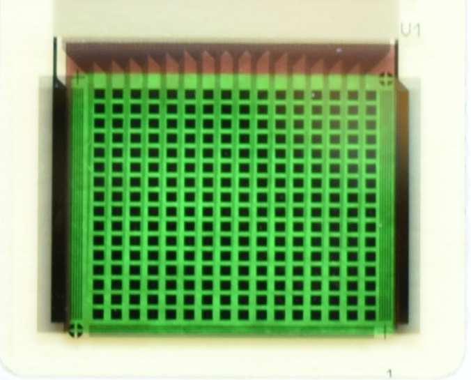
11 Semi-transparent backplane (1) Self Aligned (SA) TFT technology 8 mask step process - IGZO - Gate stack - SiN Via - SD - Interlayer - Cathode - ETL - Edge Cover Sequential processing of TFT, interlayer, OPD cathode and ETL Source Edge cover layer Gate Gate dielectric IGZO Drain Barrier Polyimide Glass ITO IGZO Interlayer Inter metal dielectric 11
12 Semi-transparent backplane (2) Reduction of mask steps by: 1. using IGZO as both the TFT contact, Edge cover layer TFT semiconductor and OPD cathode/etl 2. combining Intermetal Dielectric and Interlayer in one material Source Gate Gate dielectric IGZO Drain IGZO Barrier Polyimide IGZO Interlayer Inter metal dielectric Glass 12


13 Self aligned semi-transparent backplane 5 mask step process IGZO used as both: - TFT contact - TFT semiconductor - OPD cathode/etl Inter metal dielectric Source Interlayer Gate Gate dielectric IGZO Barrier Polyimide Glass 13

 Optimization of")

14 Large area deposition OPD blend S2S based Slot-die Coating process Homogeneous coatings on GEN1 size (320 x 352 mm) Optimization of materials, inks and coating conditions Pinhole free, homogeneous coating 14

15 Semi-transparent image sensors 15
16 Transmission measurements 1,0 top encapsulation 0,8 transparent top electrode Transmission 0,6 0,4 0,2 PI + bottom TFE SA P12 PI + bottom TFE + backplane SA P12 PI + bottom TFE + backplane *0.8 0, D IGZO bottom encapsulation OPD TFT Wavelength [nm] PI 550 nm 550 nm 70% TFT backplane 80% glass carrier 16 Albert van Breemen - Scalable self-aligned active matrix IGZO TFT backplane technologyand its use in flexible semi-transparent image sensors

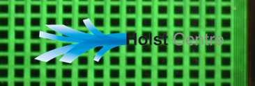
17 Semi-transparent imager movie Image sensor is turned upside down glass carrier PI foil bottom encapsulation IGZO D transparent top electrode top encapsulation TFT OPD transparency Holst Centre logo illumination 17
18 Video semi-transparent image sensor 18 Albert van Breemen - Scalable self-aligned active matrix IGZO TFT backplane technologyand its use in flexible semi-transparent image sensors

19 Near-IR (NIR) photodetectors Applications foreseen in: - pulse oximetry - biometrics - interactive surfaces 19


20 Near-IR (NIR) photodetectors Applications foreseen in: - pulse oximetry - biometrics Donor 1 Acceptor Donor 2 - interactive surfaces Spectral sensitivity of OPD can be easily tuned by changing donor polymer Donor 2 + Acceptor EQE [%] Donor 1 + Acceptor λ [nm]
")
21 Near-IR (NIR) photodetectors 16 x 16 OPD array 21
22 Video Near-IR (NIR) photodetector 22


23 Summary Semi-transparent self-aligned TFT backplanes: - IGZO facilitates the combination of specific TFT and OPD functionalities in a single material - 5 mask step scalable process - Transparency 80% Functional semi-transparent image sensors shown Near-IR photodetectors will further unleash the applications of semi-transparent image sensors Source Inter metal dielectric Interlayer Gate Gate dielectric IGZO Buffer Barrier Polyimide Glass 23 Albert van Breemen - Scalable self-aligned active matrix IGZO TFT backplane technologyand its use in flexible semi-transparent image sensors


24 Acknowledgements Holst Centre TFT pilot line team Santhosh Shanmugam Holst Centre thin film encapsulation team Hylke Akkerman Bart Peeters, Ilias Katsouras Gerwin Gelinck and many others! Bart Peeters 24

25
Flexible Electronics Production Deployment on FPD Standards: Plastic Displays & Integrated Circuits. Stanislav Loboda R&D engineer
 Flexible Electronics Production Deployment on FPD Standards: Plastic Displays & Integrated Circuits Stanislav Loboda R&D engineer The world-first small-volume contract manufacturing for plastic TFT-arrays
AMOLED Manufacturing Process Report SAMPLE
 AMOLED Manufacturing Process Report SAMPLE 2018 AMOLED Manufacturing Process Report The report analyzes the structure and manufacturing process by dividing AMOLED into small & medium-sized rigid OLED,
PROCESS TECHNOLOGIES FOR ADVANCED ORGANIC ELECTRONIC DEVICES: MICRODISPLAYS, LIGHTING AND SOLAR CELLS
 PROCESS TECHNOLOGIES FOR ADVANCED ORGANIC ELECTRONIC DEVICES: MICRODISPLAYS, LIGHTING AND SOLAR CELLS Dr. Christian May Fraunhofer IPMS - Center for Organic Materials and Electronic Devices Dresden COMEDD
Development of OLED Lighting Applications Using Phosphorescent Emission System
 Development of OLED Lighting Applications Using Phosphorescent Emission System Kazuhiro Oikawa R&D Department OLED Lighting Business Center KONICA MINOLTA ADVANCED LAYERS, INC. October 10, 2012 Outline
[1.9] AMOLED 공정 Introduction OLED Materials Patterning Process Process Equipments
![[1.9] AMOLED 공정 Introduction OLED Materials Patterning Process Process Equipments](/thumbs/73/69073032.jpg "[1.9] AMOLED 공정 Introduction OLED Materials Patterning Process Process Equipments") [1.9] AMOLED 공정 1.9.1. Introduction 1.9.2. OLED Materials 1.9.3. Patterning Process 1.9.4. Process Equipments OLED : Organic Light Emitting Diode Organic EL : Organic Electroluminescent 재료및공정 재료의발광메카니즘
[1.9] AMOLED 공정 1.9.1. Introduction 1.9.2. OLED Materials 1.9.3. Patterning Process 1.9.4. Process Equipments OLED : Organic Light Emitting Diode Organic EL : Organic Electroluminescent 재료및공정 재료의발광메카니즘
1. Publishable summary
 1. Publishable summary 1.1. Project objectives. The target of the project is to develop a highly reliable high brightness conformable low cost scalable display for demanding applications such as their
Silole Derivative Properties in Organic Light Emitting Diodes
 Silole Derivative Properties in Organic Light Emitting Diodes E. Duncan MLK HS Physics Teacher Mentors: Prof. Bernard Kippelen & Dr. Benoit Domercq Introduction Theory Methodology Results Conclusion Acknowledgements
Solution Processable OLEDs. Anna Hayer EuroDisplay /09/2013
 Solution Processable LEDs Merck KGaA Anna Hayer EuroDisplay 2013 Content 1 Introduction 2 LED Basics 3 Challenges for Solution Processing 4 Current Results 5 Summary 2 EuroDisplay 2013 Hayer - Merck Solution
Advanced Display Manufacturing Technology
 Advanced Display Manufacturing Technology John Busch Vice President, New Business Development Display and Flexible Technology Group September 28, 2017 Safe Harbor This presentation contains forward-looking
Advances in Roll-to-Roll Imprint Lithography for Display Applications Using Self Aligned Imprint Lithography. John G Maltabes HP Labs
 Advances in Roll-to-Roll Imprint Lithography for Display Applications Using Self Aligned Imprint Lithography John G Maltabes HP Labs Outline Introduction Roll to Roll Challenges and Benefits HP Labs Roll
The Company. A leading OLED player
 The Company A leading OLED player Novaled is the company to trade with, work for and invest in. Our company focuses on proprietary organic materials and complementary innovative technologies for superior
projectors, head mounted displays in virtual or augmented reality use, electronic viewfinders
 Beatrice Beyer Figure 1. (OLED) microdisplay with a screen diagonal of 16 mm. Figure 2. CMOS cross section with OLED on top. Usually as small as fingernails, but of very high resolution Optical system
Phosphorescent OLED Technologies: The Next Wave. Plastic Electronics Conference Oct 9, 2012
 Phosphorescent OLED Technologies: The Next Wave Plastic Electronics Conference Oct 9, 2012 UDC Company Focus IP innovator, technology developer, patent licensor and materials supplier for the rapidly growing
Flexible Flat Panel Display Technology
 1 Flexible Flat Panel Display Technology Gregory P. Crawford Division of Engineering, Brown University, Providence RI 1.1 Introduction The manufacturing of flat panel displays is a dynamic and continuously
OLED Status quo and our position
 OLED Status quo and our position Information Day 2013 A Deep Dive into the LC&OLED Business Dr. Udo Heider Vice President OLED Darmstadt, Germany June 26, 2013 Disclaimer Remarks All comparative figures
VARIOUS DISPLAY TECHNOLOGIESS
 VARIOUS DISPLAY TECHNOLOGIESS Mr. Virat C. Gandhi 1 1 Computer Department, C. U. Shah Technical Institute of Diploma Studies Abstract A lot has been invented from the past till now in regards with the
Advanced Sensor Technologies
 Advanced Sensor Technologies Jörg Amelung Fraunhofer Institute for Photonics Microsystems Name of presenter date Sensors as core element for IoT Next phase of market grow New/Advanced Requirements based
Joint Development of Ultra-Bright, Inorganic EL Light-Emitting Materials. November 2, 2005 KURARAY CO., LTD.
 Joint Development of Ultra-Bright, Inorganic EL Light-Emitting Materials November 2, 2005 KURARAY CO., LTD. Sales Trends of Display-related Products (Kuraray (standalone)) FY1994 FY1999 FY2004 Sales Ratio
FLEX2017 June, Monterey, USA Dr Mike Cowin, CMO, SmartKem.
 FLEX2017 June, Monterey, USA Dr Mike Cowin, CMO, SmartKem. FLEX2017 June, Monterey, USA Dr Mike Cowin, CMO, SmartKem. EU H2020 FLEXTRANs Grant Objectives A 24 month project (started September 2016) (Grant
ADDING AN O TO LEDS STATUS AND PERSPECTIVES OF ORGANIC LIGHT EMITTING DIODES PAWEL E. MALINOWSKI, TUNGHUEI KE LED EVENT 2017
 ADDING AN O TO LEDS STATUS AND PERSPECTIVES OF ORGANIC LIGHT EMITTING DIODES PAWEL E. MALINOWSKI, TUNGHUEI KE LIVING ROOM NOT SO LONG AGO... 2 Source: Warner Bros. Incadescent CRT 3 Source: Warner Bros.
 Chapter 1 Introduction --------------------------------------------------------------------------------------------------------------- 1.1 Overview of the Organic Light Emitting Diode (OLED) Displays Flat
High Power Efficiencies at Record Lifetimes: NOVALED s PIN-OLEDs
 High Power Efficiencies at Record Lifetimes: NOVALED s PIN-OLEDs Harald Gross, Jan Blochwitz-Nimoth, Jan Birnstock, Ansgar Werner, Michael Hofmann, Philipp Wellmann, Tilmann Romainczyk, Sven Murano, Andrea
High Efficiency White OLEDs for Lighting
 CIE-y Journal of Photopolymer Science and Technology Volume 25, Number 3 (2012) 321 326 2012CPST High Efficiency White OLEDs for Lighting Takuya Komoda, Kazuyuki Yamae, Varutt Kittichungchit, Hiroya Tsuji
TipatOr. Liquid metal switch (LMS) display technology. Avi Fogel
 display technology. Avi Fogel") TipatOr Liquid metal switch (LMS) display technology Avi Fogel 972-52-5702938 avifog@gmail.com Who is behind TipatOr TipatOr emerged from a merger of 2 expert groups in the fields of MEMS and Displays
TipatOr Liquid metal switch (LMS) display technology Avi Fogel 972-52-5702938 avifog@gmail.com Who is behind TipatOr TipatOr emerged from a merger of 2 expert groups in the fields of MEMS and Displays
Performance Comparison of Bilayer and Multilayer OLED
 Performance Comparison of Bilayer and Multilayer OLED Akanksha Uniyal, Poornima Mittal * Department of Electronics and Communication School of Engineering and Technology Graphic Era University, Dehradun-248002,
An Overview of OLED Display Technology
 page:1 An Overview of OLED Display Technology Homer Antoniadis OSRAM Opto Semiconductors Inc. San Jose, CA page:2 Outline! OLED device structure and operation! OLED materials (polymers and small molecules)!
UniMCO 4.0: A Unique CAD Tool for LED, OLED, RCLED, VCSEL, & Optical Coatings
 UniMCO 4.0: A Unique CAD Tool for LED, OLED, RCLED, VCSEL, & Optical Coatings 1 Outline Physics of LED & OLED Microcavity LED (RCLED) and OLED (MCOLED) UniMCO 4.0: Unique CAD tool for LED-Based Devices
Quantum Dot Solutions for Lighting and Display Applications. Frank Ignazzitto APEC Conference February 9, 2012
 Quantum Dot Solutions for Lighting and Display Applications Frank Ignazzitto APEC Conference February 9, 2012 QD Vision s Focused & Integrated Approach The only quantum dot company focused solely on displays
Organic light emitting diode (OLED) displays
 displays") Ultra-Short Pulse Lasers Enable Precision Flexible OLED Cutting FLORENT THIBAULT, PRODUCT LINE MANAGER, HATIM HALOUI, APPLICATION MANAGER, JORIS VAN NUNEN, PRODUCT MARKETING MANAGER, INDUSTRIAL PICOSECOND
Ultra-Short Pulse Lasers Enable Precision Flexible OLED Cutting FLORENT THIBAULT, PRODUCT LINE MANAGER, HATIM HALOUI, APPLICATION MANAGER, JORIS VAN NUNEN, PRODUCT MARKETING MANAGER, INDUSTRIAL PICOSECOND
Semiconductors Displays Semiconductor Manufacturing and Inspection Equipment Scientific Instruments
 Semiconductors Displays Semiconductor Manufacturing and Inspection Equipment Scientific Instruments Electronics 110-nm CMOS ASIC HDL4P Series with High-speed I/O Interfaces Hitachi has released the high-performance
FASwitch - A MEMS Display Backplane Manufactured by Flex Circuit Methods
 FASwitch - A MEMS Display Backplane Manufactured by Flex Circuit Methods Presenter: Dr. Nicholas F. Pasch Rolltronics Corporation 750 Menlo Ave. Menlo Park, CA 94025 npasch@rolltronics.com Introduction
Solution-based transistor matrix
 18 PRINTED ELECTRONICS Solution-based transistor matrix A groundbreaking new technology is making it far more cost-effective to produce the electronic control unit of liquid crystal displays. At the same
Liquid Crystal Display (LCD)
") Liquid Crystal Display (LCD) When coming into contact with grooved surface in a fixed direction, liquid crystal molecules line up parallelly along the grooves. When coming into contact with grooved surface
Liquid Crystal Display (LCD) When coming into contact with grooved surface in a fixed direction, liquid crystal molecules line up parallelly along the grooves. When coming into contact with grooved surface
DESIGN OF VISIBLE LIGHT COMMUNICATION SYSTEM
 DESIGN OF VISIBLE LIGHT COMMUNICATION SYSTEM *Vishakh B V, **Mohammed Kamal Khwaja *School of Electronics Engineering, VIT University, Vellore, India ** School of Electronics Engineering, VIT University,
Design of Organic TFT Pixel Electrode Circuit for Active-Matrix OLED Displays
 JOURNAL OF COMPUTERS, VOL. 3, NO. 3, MARCH 2008 1 Design of Organic TFT Pixel Electrode Circuit for Active-Matrix Displays Aram Shin, Sang Jun Hwang, Seung Woo Yu, and Man Young Sung 1) Semiconductor and
Organic Light Emitting Diodes
 ISSN: 2278 0211 (Online) Organic Light Emitting Diodes Badisa Sai Ram Krsihna Final Year B.Tech, Dept. of ECE, KL University, Vaddeswaram, AP, India Angadi Suresh Associate Professor B.Tech, Dept. of ECE,
Thin-Film Encapsulation of Organic Light Emitting Devices (OLEDs) Dr. Emilie Galand Huntsman Advanced Materials CSEM Plastic Optoelectronics - Basel
 Dr. Emilie Galand Huntsman Advanced Materials CSEM Plastic Optoelectronics - Basel") Thin-Film Encapsulation of Organic Light Emitting Devices (OLEDs) Dr. Emilie Galand CSEM Plastic Optoelectronics - Basel 25th June 2010 About Huntsman Huntsman is a global manufacturer and marketer of
Thin-Film Encapsulation of Organic Light Emitting Devices (OLEDs) Dr. Emilie Galand CSEM Plastic Optoelectronics - Basel 25th June 2010 About Huntsman Huntsman is a global manufacturer and marketer of
COMPENSATION FOR THRESHOLD INSTABILITY OF THIN-FILM TRANSISTORS
 COMPENSATION FOR THRESHOLD INSTABILITY OF THIN-FILM TRANSISTORS by Roberto W. Flores A Thesis Submitted to the Graduate Faculty of George Mason University in Partial Fulfillment of The Requirements for
Content. Core Technology (Short introduction) LCMO (Light Controlled Molecular Orientation) technology
 LCMO (Light Controlled Molecular Orientation) technology") Content Core Technology (Short introduction) LCMO (Light Controlled Molecular Orientation) technology LCMO Patterned Films for Light management : Applications Examples LCMO- Photo Patterned Retarders LCMO-
Content Core Technology (Short introduction) LCMO (Light Controlled Molecular Orientation) technology LCMO Patterned Films for Light management : Applications Examples LCMO- Photo Patterned Retarders LCMO-
OLED Technology Introduction
 OLED Technology Introduction An organic light emitting diode (OLED) consists of several semiconducting organic layers sandwiched between two electrodes at least one of them being transparent. A simplified
The Technological Trends of Future AMOLED
 Invited Paper The Technological Trends of Future AMOLED Jong hyuk Lee*, Hye Dong Kim, Chang Ho Lee, Hyun-Joong Chung, Sung Chul Kim, and Sang Soo Kim Technology Center, Samsung Mobile Display Co., LTD
IOSR Journal of Engineering (IOSRJEN) ISSN (e): , ISSN (p): Volume 2, PP Organic Led. Figure 1.
 ISSN (e): , ISSN (p): Volume 2, PP Organic Led. Figure 1.") IOSR Journal of Engineering (IOSRJEN) ISSN (e): 2250-3021, ISSN (p): 2278-8719 Volume 2, PP 46-51 www.iosrjen.org Organic Led Prof.Manoj Mishra 1, Sweety Vade 2,Shrutika Sawant 3, Shriwari Shedge 4, Ketaki
IOSR Journal of Engineering (IOSRJEN) ISSN (e): 2250-3021, ISSN (p): 2278-8719 Volume 2, PP 46-51 www.iosrjen.org Organic Led Prof.Manoj Mishra 1, Sweety Vade 2,Shrutika Sawant 3, Shriwari Shedge 4, Ketaki
Emiflective Display with Integration of Reflective Liquid Crystal Display and Organic Light Emitting Diode
 Japanese Journal of Applied Physics Vol. 46, No. 1, 2007, pp. 182 186 #2007 The Japan Society of Applied Physics Emiflective Display with Integration of Reflective Liquid Crystal Display and Organic Light
P I SCALE Creating an Open Access Flexible O L E D P ilo t L in e S e r vic e
 P I SCALE Creating an Open Access Flexible O L E D P ilo t L in e S e r vic e Pavel Kudlacek pavel.kudlacek@tno.nl P I - SCALE for 2017Flex 1 Lighting c h a lle n g e L ig h t in g c h a lle n g e At least
Solid State Devices 4B6
 Solid State Devices 4B6 Lecture 13 Projection and 3D displays: LCD, DLP and LCOS Daping Chu Lent 2016 Development of flat panel displays (FPDs) (LCD) in early days 1 A 105 inch TFT-LCD 4k2k curved panel
Challenges in the design of a RGB LED display for indoor applications
 Synthetic Metals 122 (2001) 215±219 Challenges in the design of a RGB LED display for indoor applications Francis Nguyen * Osram Opto Semiconductors, In neon Technologies Corporation, 19000, Homestead
Stacked OLEDs for Lighting Applications - Improvement of the yellow building block
 Stacked OLEDs for Lighting Applications Improvement of the yellow building block 13/12/2010 Carola Diez Osram Opto Semiconductors GmbH and University of Augsburg OLED Lighting White organic light emitting
Organic light emitting diodes for display technology
 Organic light emitting diodes for display technology Shamna Shamsudeen MScTI - ZITI-Heidelberg University OLED ZITI, Uni Heidelberg Page1 What s Light Light: Visible part of EM spectra. Ref:[1] Thermoluminescence:
High contrast tandem organic light emitting devices employing transparent intermediate nano metal layers and a phase shifting layer
 Edith Cowan University Research Online ECU Publications 2012 2012 High contrast tandem organic light emitting devices employing transparent intermediate nano metal layers and a phase shifting layer Baofu
The promise of organic electronics previously-unimaginable innovative products
 white paper for trade show visitors The promise of organic electronics previously-unimaginable innovative products The productronica trade show (Nov 10-13, 2009, Munich) will provide additional information
AIXTRON in EXCILIGHT project
 AIXTRON SE AIXTRON in EXCILIGHT project Gintautas Simkus ABOUT AIXTRON 2 Who we are Headquarter based in Herzogenrath, Germany Worldwide presence with 14 sales/representatives offices and production facilities
ORGANIC ELECTRONICS PROCESS DEVELOPMENT AND ENCAPSULATION TECHNOLOGIES
 FRAUNHOFER INSTITUTE FOR ORGANIC ELECTRONICS, ELECTRON BEAM AND PLASMA TECHNOLOGY FEP ORGANIC ELECTRONICS PROCESS DEVELOPMENT AND ENCAPSULATION TECHNOLOGIES 2 PROFILE Fraunhofer FEP combines research and
CCD 143A 2048-Element High Speed Linear Image Sensor
 A CCD 143A 2048-Element High Speed Linear Image Sensor FEATURES 2048 x 1 photosite array 13µm x 13µm photosites on 13µm pitch High speed = up to 20MHz data rates Enhanced spectral response Low dark signal
P-224: Damage-Free Cathode Coating Process for OLEDs
 P-224: Damage-Free Cathode Coating Process for OLEDs Shiva Prakash DuPont Displays, 6 Ward Drive, Santa Barbara, CA 937, USA Abstract OLED displays require the growth of inorganic films over organic films.
Introduction... 4 About the author... 6 What is an OLED? OLED: An Organic Light Emitting Device... 7 Different kinds of OLEDs...
 Table of Contents Introduction... 4 About the author... 6 What is an OLED?... 7 OLED: An Organic Light Emitting Device... 7 Different kinds of OLEDs... 9 How an OLED display is made... 14 The backplane...
In-Cell Projected Capacitive Touch Panel Technology
 1384 INVITED PAPER Special Section on Electronic Displays In-Cell Projected Capacitive Touch Panel Technology Yasuhiro SUGITA a), Member, Kazutoshi KIDA, and Shinji YAMAGISHI, Nonmembers SUMMARY We describe
SPATIAL LIGHT MODULATORS
 SPATIAL LIGHT MODULATORS Reflective XY Series Phase and Amplitude 512x512 A spatial light modulator (SLM) is an electrically programmable device that modulates light according to a fixed spatial (pixel)
ORGANIC LIGHT EMITTING DIODES (OLEDS): TECHNOLOGIES AND GLOBAL MARKETS
: TECHNOLOGIES AND GLOBAL MARKETS") ORGANIC LIGHT EMITTING DIODES (OLEDS): TECHNOLOGIES AND GLOBAL MARKETS SMC069D September 2015 Gupta A. S. Project Analyst ISBN: 1-62296-133-1 BCC Research 49 Walnut Park, Building 2 Wellesley, MA 02481
ORGANIC LIGHT EMITTING DIODES (OLEDS): TECHNOLOGIES AND GLOBAL MARKETS SMC069D September 2015 Gupta A. S. Project Analyst ISBN: 1-62296-133-1 BCC Research 49 Walnut Park, Building 2 Wellesley, MA 02481
An Introduction to OLED/TFT Device Model and FPD Design Flow
 An Introduction to OLED/TFT Device Model and FPD Design Flow Lifeng Wu, Huada Empyrean Software MOS-AK Beijing Compact Modeling Workshop,June 15-16, 2018 1 Outline LCD and OLED Flat Panel Display (FPD)
Overview of All Pixel Circuits for Active Matrix Organic Light Emitting Diode (AMOLED)
") Chapter 2 Overview of All Pixel Circuits for Active Matrix Organic Light Emitting Diode (AMOLED) ---------------------------------------------------------------------------------------------------------------
Chapter 2 Overview of All Pixel Circuits for Active Matrix Organic Light Emitting Diode (AMOLED) ---------------------------------------------------------------------------------------------------------------
VG5761, VG5661 VD5761, VD5661 Data brief
 VG5761, VG5661 VD5761, VD5661 Data brief Automotive 1.6-2.3 megapixel high-dynamic global shutter image sensor Features Product summary Root part number Resolution (megapixel) Package VG5661 1.6 IM2BGA
Spatial Light Modulators XY Series
 Spatial Light Modulators XY Series Phase and Amplitude 512x512 and 256x256 A spatial light modulator (SLM) is an electrically programmable device that modulates light according to a fixed spatial (pixel)
InvenSense Fabless Model for the MEMS Industry
 InvenSense Fabless Model for the MEMS Industry HKSTP Symposium Aug 2016 InvenSense, Inc. Proprietary Outline MEMS Market InvenSense CMOS-MEMS Integration InvenSense Shuttle Program and Process MEMS MARKET
Sep 09, APPLICATION NOTE 1193 Electronic Displays Comparison
 Sep 09, 2002 APPLICATION NOTE 1193 Electronic s Comparison Abstract: This note compares advantages and disadvantages of Cathode Ray Tubes, Electro-Luminescent, Flip- Dot, Incandescent Light Bulbs, Liquid
Display Technologies CMSC 435. Slides based on Dr. Luebke s slides
 Display Technologies CMSC 435 Slides based on Dr. Luebke s slides Recap: Transforms Basic 2D Transforms: Scaling, Shearing, Rotation, Reflection, Composition of 2D Transforms Basic 3D Transforms: Rotation,
FIRST CALL FOR PAPERS SID Society for Information Display INTERNATIONAL SYMPOSIUM, SEMINAR & EXHIBITION. May 19 24, 2013
 FIRST CALL FOR PAPERS SID 2013 Society for Information Display INTERNATIONAL SYMPOSIUM, SEMINAR & EXHIBITION May 19 24, 2013 VANCOUVER CONVENTION CENTER VANCOUVER, BRITISH COLUMBIA, CANADA SID SOCIETY
Gary Mandle Sr. Product Manager Professional Display Products
 Gary Mandle Sr. Product Manager Professional Display Products rganic Light Emitting Diode It is: An emissive output o backlight o plasma gasses Self luminous matrix array Created by sandwiching several
Comparative Analysis of Organic Thin Film Transistor Structures for Flexible E-Paper and AMOLED Displays
 Comparative Analysis of Organic Thin Film Transistor Structures for Flexible E-Paper and AMOLED Displays Linrun Feng, Xiaoli Xu and Xiaojun Guo ECS Trans. 2011, Volume 37, Issue 1, Pages 105-112. doi:
SEMICONDUCTOR TECHNOLOGY -CMOS-
 SEMICONDUCTOR TECHNOLOGY -CMOS- Fire Tom Wada 2011/12/19 1 What is semiconductor and LSIs Huge number of transistors can be integrated in a small Si chip. The size of the chip is roughly the size of nails.
(12) Patent Application Publication (10) Pub. No.: US 2015/ A1
 Patent Application Publication (10) Pub. No.: US 2015/ A1") (19) United States US 20150379938A1 (12) Patent Application Publication (10) Pub. No.: US 2015/0379938A1 (21) (22) (60) (51) Choi et al. (43) Pub. Date: Dec. 31, 2015 (54) ORGANIC LIGHT-EMITTING DIODE
(19) United States US 20150379938A1 (12) Patent Application Publication (10) Pub. No.: US 2015/0379938A1 (21) (22) (60) (51) Choi et al. (43) Pub. Date: Dec. 31, 2015 (54) ORGANIC LIGHT-EMITTING DIODE
Exhibits. Open House. NHK STRL Open House Entrance. Smart Production. Open House 2018 Exhibits
 2018 Exhibits NHK STRL 2018 Exhibits Entrance E1 NHK STRL3-Year R&D Plan (FY 2018-2020) The NHK STRL 3-Year R&D Plan for creating new broadcasting technologies and services with goals for 2020, and beyond
Process Dependent Performance of Slot Die Coated OLED-Multilayers (TALK)
") Process Dependent Performance of Slot Die Coated OLED-Multilayers (TALK) Sebastian Raupp 1,2, Lisa Merklein 1,2, Philip Scharfer 1,2 and Wilhelm Schabel 1 1 Institute of Thermal Process Engineering, Thin
Process Dependent Performance of Slot Die Coated OLED-Multilayers (TALK) Sebastian Raupp 1,2, Lisa Merklein 1,2, Philip Scharfer 1,2 and Wilhelm Schabel 1 1 Institute of Thermal Process Engineering, Thin
High Performance White OLEDs Technologies for Lighting
 High Performance White OLEDs Technologies for Lighting 10 October, 2012 Takuya Komoda Core Technologies Development Center Panasonic Corporation Contents 2 1. Expectation to the Next Generation Lighting
Alien Technology Corporation White Paper. Fluidic Self Assembly. October 1999
 Alien Technology Corporation White Paper Fluidic Self Assembly October 1999 Alien Technology Corp Page 1 Why FSA? Alien Technology Corp. was formed to commercialize a proprietary technology process, protected
Fundamentals of Organic Light Emitting Diode
 Fundamentals of Organic Light Emitting Diode M. F. Rahman* 1 and M. Moniruzzaman 2 Organic light emitting diode (OLED) has drawn tremendous attention in optoelectronic industry over the last few years.
17. Optical detectors and displays. Optical displays. FPD (Flat panel display)
") 17. Optical detectors and displays Optical displays FPD (Flat panel display) Display Resolutions High-definition television (HDTV): 720p (1280 720 progressive scan) 1080i (1920 1080 split into two interlaced
17. Optical detectors and displays Optical displays FPD (Flat panel display) Display Resolutions High-definition television (HDTV): 720p (1280 720 progressive scan) 1080i (1920 1080 split into two interlaced
HAPD and Electronics Updates
 S. Nishida KEK 3rd Open Meeting for Belle II Collaboration 1 Contents Frontend Electronics Neutron Irradiation News from Hamamtsu 2 144ch HAPD HAPD (Hybrid Avalanche Photo Detector) photon bi alkali photocathode
Advancement in the Technology of Organic Light Emitting Diodes
 IOSR Journal of Electrical and Electronics Engineering (IOSR-JEEE) e-issn: 2278-1676,p-ISSN: 2320-3331, PP 06-10 www.iosrjournals.org Advancement in the Technology of Organic Light Emitting Diodes Rohan
center for organic materials and electronic devices dresden
 F R A U N H O F E R I N S T I T U T e F o R P h o t o n i c M i c r o S y s t e m s I P M S center for organic materials and electronic devices dresden p r e f a c e Dr. Christian May Head of Business
SEMICONDUCTOR TECHNOLOGY -CMOS-
 SEMICONDUCTOR TECHNOLOGY -CMOS- Fire Tom Wada What is semiconductor and LSIs Huge number of transistors can be integrated in a small Si chip. The size of the chip is roughly the size of nails. Currently,
Defect Analysis of Roll-to-Roll SAIL Manufactured Flexible Display Backplanes
 Defect Analysis of Roll-to-Roll SAIL Manufactured Flexible Display Backplanes Carl Taussig, Richard E. Elder, Warren B. Jackson, Albert Jeans, Mehrban Jam, Ed Holland, Hao Luo, John Maltabes, Craig Perlov,
LED Display Backlighting Monitor Applications using 6-lead MULTILED Application Note
 LED Display Backlighting Monitor Applications using 6-lead MULTILED Application Note Abstract This application note describes two reference designs for LCD backlighting using the 6-lead MULTILED LRTB G6SG.
Advanced Display Technology (continued) Lecture 13 October 4, 2016 Imaging in the Electronic Age Donald P. Greenberg
 Lecture 13 October 4, 2016 Imaging in the Electronic Age Donald P. Greenberg") Advanced Display Technology (continued) Lecture 13 October 4, 2016 Imaging in the Electronic Age Donald P. Greenberg Cost of HDTV Displays Price $ Plasma Projection TV s LCD s Diagonal Inches Cost of HDTV
Advanced Display Technology (continued) Lecture 13 October 4, 2016 Imaging in the Electronic Age Donald P. Greenberg Cost of HDTV Displays Price $ Plasma Projection TV s LCD s Diagonal Inches Cost of HDTV
OLED ON CMOS: WHAT ABOUT THINNING AND BENDING?
 Large cost-effective OLED microdisplays and their applications OLED ON CMOS: WHAT ABOUT THINNING AND BENDING? IDW2017 tony.maindron@cea.fr T. Maindron, B. Chambion, A. Vandeneynde, S. Gétin, M. Provost,
New Worlds for Polymers: Organic Transistors, Light Emitting Diodes, and Optical Waveguides Ed Chandross
 New Worlds for Polymers: Organic Transistors, Light Emitting Diodes, and Optical Waveguides Ed Chandross Materials Chemistry, LLC 1 Polymers in the Electronic Industry Enabling Materials Active Materials?
OLED COMPANY. for Display & Lighting Applications
 OLED COMPANY for Display & Lighting Applications Novaled: World-class OLED Player Novaled creates value for OLED (Organic Light Emitting Diode) and Organic Electronics (OE) makers. Novaled s PIN technology
(12) United States Patent
 United States Patent") US00926.3506B2 (12) United States Patent Kim (10) Patent No.: (45) Date of Patent: US 9.263,506 B2 Feb. 16, 2016 (54) ORGANIC LIGHT EMITTING DIODE (OLED) DISPLAY INCLUDING CURVED OLED (71) Applicant: SAMSUNG
US00926.3506B2 (12) United States Patent Kim (10) Patent No.: (45) Date of Patent: US 9.263,506 B2 Feb. 16, 2016 (54) ORGANIC LIGHT EMITTING DIODE (OLED) DISPLAY INCLUDING CURVED OLED (71) Applicant: SAMSUNG
High Repetition Rate USP Lasers Improve OLED Cutting Results
 Coherent White Paper May 7, 2018 High Repetition Rate USP Lasers Improve OLED Cutting Results High power ultraviolet, picosecond industrial lasers are widely employed because of their proven ability to
Flat Panel Displays: LCD Technologies and Trends
 Flat Panel Displays: LCD Technologies and Trends Robert Dunhouse, Sr. Engineering Manager, Display BU Class ID: 4C01B Renesas Electronics America Inc. Robert F. Dunhouse, Jr. Sr. Engineering Manager, Display
(12) Patent Application Publication (10) Pub. No.: US 2016/ A1
 Patent Application Publication (10) Pub. No.: US 2016/ A1") (19) United States US 2016O141348A1 (12) Patent Application Publication (10) Pub. No.: US 2016/0141348 A1 Lin et al. (43) Pub. Date: May 19, 2016 (54) ORGANIC LIGHT-EMITTING DIODE (52) U.S. Cl. DISPLAY
(19) United States US 2016O141348A1 (12) Patent Application Publication (10) Pub. No.: US 2016/0141348 A1 Lin et al. (43) Pub. Date: May 19, 2016 (54) ORGANIC LIGHT-EMITTING DIODE (52) U.S. Cl. DISPLAY
:: Reduce needs for heat dissipation components. :: Extend battery life in mobile products. :: Save power and reduce heat generation in TVs
 UniversalPHOLED Technology and Materials UniversalPHOLED Phosphorescent OLED technology and materials offer record-breaking performance to bring competitive advantages to your OLED display and lighting
 Chapter 3 Evaluated Results of Conventional Pixel Circuit, Other Compensation Circuits and Proposed Pixel Circuits for Active Matrix Organic Light Emitting Diodes (AMOLEDs) -------------------------------------------------------------------------------------------------------
Displays and framebuffers
 Reading Optional Displays and framebuffers Brian Curless CSE 557 Autumn 2017 OpenGL Programming Guide (the red book available online): First four sections of chapter 2 First section of chapter 6 Foley
ID C10C: Flat Panel Display Basics
 ID C10C: Flat Panel Display Basics Renesas Electronics America Inc. Robert Dunhouse, Display BU Engineering Manager 12 October 2010 Revision 1.1 Robert F. Dunhouse, Jr. Displays Applications Engineering
Technology White Paper Plasma Displays. NEC Technologies Visual Systems Division
 Technology White Paper Plasma Displays NEC Technologies Visual Systems Division May 1998 1 What is a Color Plasma Display Panel? The term Plasma refers to a flat panel display technology that utilizes
 Page 1 of 8 Main > Electronics > Computers How OLEDs Work by Craig Freudenrich, Ph.D. Introduction to How OLEDs Work Imagine having a high-definition TV that is 80 inches wide and less than a quarter-inch
Light, Bright, and. Julie Brown Universal Display Corporation.
 Light, Bright, and Julie Brown Universal Display Corporation jjbrown@universaldisplay.com May 3, 2006 A Perspective OLEDs Yesterday OLEDs Today OLEDs Tomorrow Milestones in OLEDs (1960-2000) 1963 Pope
CCD Element Linear Image Sensor CCD Element Line Scan Image Sensor
 1024-Element Linear Image Sensor CCD 134 1024-Element Line Scan Image Sensor FEATURES 1024 x 1 photosite array 13µm x 13µm photosites on 13µm pitch Anti-blooming and integration control Enhanced spectral
The future of microled displays using nextgeneration
 The future of microled displays using nextgeneration technologies Introduction MicroLEDs (micro-light-emitting diodes) are an emerging display technology that, as the name implies, use very small LEDs