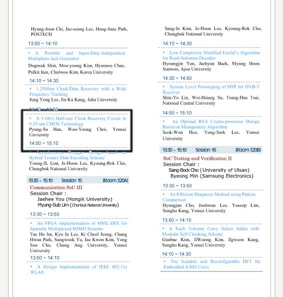
A 5-Gb/s Half-rate Clock Recovery Circuit in 0.25-μm CMOS Technology
|
|
|
- Jack Lyons
- 5 years ago
- Views:
Transcription
1
2
3 A 5-Gb/s Half-rate Clock Recovery Circuit in 0.25-μm CMOS Technology Pyung-Su Han Dept. of Electrical and Electronic Engineering Yonsei University Seoul, Korea Woo-Young Choi Dept. of Electrical and Electronic Engineering Yonsei University Seoul, Korea Abstract A half-rate clock recovery circuit for 5-Gb/s data rate was designed in 0.25-μm CMOS technology. The bang-bang phase detector was used for high-speed operation. The simulation results show that the half-rate clock was successfully extracted from random bit data sequence up to 6-Gb/s. In initial measurement of the fabricated chip, 2.5-GHz clock was extracted from 2.5- Gb/s PRBS Further measurement will be done and presented. Keywords: Bang-bang phase detector, BBPD, Half-rate clock recovery 1 Introduction BBPD (Bang-Bang Phase Detector) is widely used for high-speed clock recovery circuits [1]. Because of its simple structure, it can operate at very high frequencies and has become an essential building block in a serial link system where data rate is extremely high. Half-rate clocking is another popular technique for high-speed data transmission applications. Using both rising and falling edges of clock, a circuit can process two bits in one clock period, doubling the data-rate without increasing the clock frequency. Adopting two techniques at the same time [2], very high-speed clock recovery circuits can be designed. The conventional PLL (phase-locked loop) model can not be used for BBPLL (Bang-Bang Phase-Locked Loop) because of BBPLL nonlinearity. Instead, the BBPLL model proposed in [1] can be used. An example of BBPLL schematic diagram is shown in Fig. 1. The voltage drop across the resistor caused by the charge pump current makes an instantaneous frequency jump in the output clock. The output clock phase change due to the frequency jump can be calculated by integrating frequency jump over time, as expressed in (1). Then this current is accumulated in the capacitor, and it generates a voltage slope. This also causes phase change in output clock. It is expressed in (2). T is the clock period. According to [1], to achieve stability in a BBPLL, (1) should be much larger than (2) by a factor of more than 20. R Figure 1. An example of BBPLL schematic diagram = πk I RT (1) θ 2 T VCO CP 2 I K I T CP π VCO CP θ C = 2π KVCO t dt = (2) C C 0 2 Building blocks All building blocks except for charge pumps and differential-to-single converters are designed with fully differential circuits for high-speed operation. 2.1 VCO A VCO delay cell and its bias circuit were designed. They are shown in Fig. 2. Two control voltages are used for its coarse and fine control, so that a wide oscillation range can be achieved, while VCO gain is kept low. Figure 2. VCO delay cell and bias circuit
4 The coarse tuning voltage, Vcntc, is determined by an external bias current Icntc and it is used for initial frequency acquisition. After frequency acquisition, it can be kept fixed. Then Vcnt finely controls output clock frequency. To achieve a low VCO gain and a larege tuning range at the same time, M1 is sized much larger than M2. Vcpt is generated using a copy of VCO cell bias current so that output swing level is relatively constant over wide VCO tuning ranges. 2.2 VCO A four-stage ring oscillator was designed with the delay cells and it is shown in Fig. 3. It generates two clock signals of which phases are separated by 90. That is, Clk_I is in-phase clock and Clk_Q is quadrature clock. Buffers are used to isolate capacitive loads at the delay cells output from the circuits connected to the VCO. Clk_Q come in the same data bit interval, therefore A and C have the same logic value. 75% of Up signal (B C) in a clock period becomes high if the B and C are different. If data bits stay unchanged, it becomes low. 25% of Up and Dn signals can be regarded as random values and in a long term, and they will eventually cancel out. In case that clock leads data, it works in the opposite way. As a result, when data bit switches, the direction of phase error is observed in Up and Dn signals. The effective gain of the half-rate BBPD is smaller by a factor of than original BBPD in BBPLL, assuming that the possibility of data bit switching is 50% 2.3 BBPD Figure 3. I/Q clock generating VCO Fig. 4 shows designed half-rate BBPD. Data bits are sampled using Clk_I and Clk_Q. Sampled data bits, A, B and C are compared by XOR gates to determine whether the clock phase is faster or slower than data bits, generating Up and Dn signals. Figure 5. Operation of half-rate BBPD 2.4 Charge pump Fig. 6 shows the designed charge pump. To minimize the mismatch between Up and Dn currents, a feedback amplifier is used [3]. It makes the voltages at output node (Vcnt) and node xx the same, trying to make both sides of charge pump have the same bias condition. By doing this, usable range of Vcnt can be extended dramatically. Cc is added for feedback loop stability. Figure 4. Half-rate bang-bang phase detector using I/Q clock Fig. 5 shows detailed signal waveforms of half-rate BBPD in operation. When the loop is locked, rising and falling edges of Clk_I are at the center of bit intervals and rising edges of Clk_Q are at bit boundaries. When clock lags behind data, 75% of Dn signal (A C) in a clock period becomes low, because rising edges of Clk_I and Figure 6. Charge pump and bias circuit 2.5 Clock recovery circuit Using building blocks described in the previous sections, a half-rate clock recovery circuit was designed.

 technique. Figure 7.")
5 Its schematic diagram is shown in Fig. 7. Because the BBPD shown in Fig. 5 detects phase error based on even numbered bits, D0, D2, D4, and so on, it utilizes only half of data transitions. As shown in Fig. 7, another BBPD for odd numbered bits, D1, D3, D5, and so on, was used. 4 Prototype chip The circuit was fabricated with 0.25-μm CMOS technology. A photograph of the prototype chip is shown in Fig. 9. The core area occupies an area of 320μm 130μm. The prototype chip was glued on a test circuit board and their terminals were connected using bondingwires by COB (Chip On Board) technique. Figure 7. Schematic diagram of clock and data recovery circuit R and C values for the loop filter were determined using (1) and (2) and their values are shown in Table. 1. Table 1. Loop filter parameters VCO gain 500MHz/V θ R 0.5% R for loop filter 500Ω θ R /θc More than 100 C for loop filter 120pF 3 Simulation results The circuit was designed with 0.25-μm CMOS technology. Its operation was verified by SPICE simuation. Considering parasitic effects, 6-Gb/s random bit sequence was used for data input, which is 20% faster than target speed, 5Gb/s. Fig. 8 shows recovered clock signal overlapped with a input data eye-diagram. Figure 9. Prototype chip photograph 5 Measurement results Figure 8. Recovered clock from 6-Gb/s random bit sequence and input data eye-diagram Figure 10. Mesured plot of control voltage to oscillation frequency transfer of fabricated VCO, depending on its coarse tuning voltage The VCO oscillation frequency range of prototype chip was measured and plotted in Fig. 10. Frequency was measured using a spectrum analyzer while the coarse and fine control voltages were being swept. Each curve on Fig. 10 represents a coarse control voltage as shown in the legend. VCO gains for each curve were also calculated and plotted in Fig. 11. It ranges from 150MHz/V to 550MHz/V.

6 Table 2. Performance summary Technology 0.25-μm CMOS Chip Area Core : 320-μm 130-μm VCO freq. range 1.65-GHz ~ 3.5-GHz VCO gain 150-MHz/V ~ 550MHz/V 2.5GHz 2.5Ghz RMS jitter : 10.7ps with PRBS P2P jitter : 69ps Power Core : 22.5mW consumption Input/output buffer : 250mW Figure 11. Measured VCO gain curve depending on coarse tuning voltage 6 Conclusions A half-rate clock recovery circuit using a bang-bang phase detector was designed with 0.25-μm CMOS technology. Its operation was verified by SPICE simulation. A prototype chip was fabricated. In initial measurement, a half-speed data pattern was used as input data and 2.5-GHz clock was sucessfully extracted from 2.5-Gb/s PRBS. Further measurement including clock recovery from 5-Gb/s bit stream will be done and the results will be presented. 7 Acknoldgement This work was sponsored in part by the Ministry of Science and Technology of Korea and the Ministry of Commerce, Industry and Energy through System IC 2010 program. Also, EDA software used in this work was supported by IDEC (IC Design Education Center). References [1] R. C. Walker, Designing bang-bang PLLs for clock and data recovery in serial data transmission systems, in Phase-Locking in High-Performance Systems, B. Razavi, Ed: Wiley-IEEE Press, 2003, pp Figure 12. Recovered clock 2.5GHz, from 2.5-Gb/s PRBS In the initial measurement, the clock recovery operation was verified using half-speed data bit pattern as input data. 2.5-GHz clock signal was successfully extracted from 2.5-Gb/s data signal. Every single bit in a half-speed bit sequence is seen as identical two bits for the clock recovery circuit. This effectively reduces clock recovery circuit s loop gain to half. Fig. 12 shows recovered clock from 2.5-Gb/s PRBS. Measured jitter was 10.7ps [rms] and 69ps [p2p]. Table 2 summarizes measurement results. Full-rate clock recovery measurement using 5-Gb/s bit sequence will be done and its results will be presented. [2] Yinghua Qiu, Zhigong Wang, Yong Xu, Jingfeng Ding, En Zhu, Mingzhen Xiong, 5-Gb/s 0.18-μm CMOS clock recovery circuit, VLSI Design and Video Technology, 2005, Proceedings of 2005 International Workshop on, May 2005, pp [3] Jae Shin Lee, Woo Kang Jin, Dong Myung Choi, Gun Sang Lee, Suki Kim, A wide range PLL for 64x speed CD-ROM & 10x speed DVD-ROM, Consumer Electronics, ICCE Digest of Technical Papers. International Conference on, June 2000, pp
A low jitter clock and data recovery with a single edge sensing Bang-Bang PD
 LETTER IEICE Electronics Express, Vol.11, No.7, 1 6 A low jitter clock and data recovery with a single edge sensing Bang-Bang PD Taek-Joon Ahn, Sang-Soon Im, Yong-Sung Ahn, and Jin-Ku Kang a) Department
INTERNATIONAL JOURNAL OF ELECTRONICS AND COMMUNICATION ENGINEERING & TECHNOLOGY (IJECET)
") INTERNATIONAL JOURNAL OF ELECTRONICS AND COMMUNICATION ENGINEERING & TECHNOLOGY (IJECET) Proceedings of the 2 nd International Conference on Current Trends in Engineering and Management ICCTEM -2014 ISSN
INTERNATIONAL JOURNAL OF ELECTRONICS AND COMMUNICATION ENGINEERING & TECHNOLOGY (IJECET) Proceedings of the 2 nd International Conference on Current Trends in Engineering and Management ICCTEM -2014 ISSN
PAPER A 1.25-Gb/s Digitally-Controlled Dual-Loop Clock and Data Recovery Circuit with Enhanced Phase Resolution
 IEICE TRANS. ELECTRON., VOL.E90 C, NO.1 JANUARY 2007 165 PAPER A 1.25-Gb/s Digitally-Controlled Dual-Loop Clock and Data Recovery Circuit with Enhanced Phase Resolution Chang-Kyung SEONG a), Seung-Woo
Efficient 500 MHz Digital Phase Locked Loop Implementation sin 180nm CMOS Technology
 Efficient 500 MHz Digital Phase Locked Loop Implementation sin 180nm CMOS Technology Akash Singh Rawat 1, Kirti Gupta 2 Electronics and Communication Department, Bharati Vidyapeeth s College of Engineering,
ECEN620: Network Theory Broadband Circuit Design Fall 2014
 ECEN620: Network Theory Broadband Circuit Design Fall 2014 Lecture 12: Divider Circuits Sam Palermo Analog & Mixed-Signal Center Texas A&M University Announcements & Agenda Divider Basics Dynamic CMOS
EL302 DIGITAL INTEGRATED CIRCUITS LAB #3 CMOS EDGE TRIGGERED D FLIP-FLOP. Due İLKER KALYONCU, 10043
 EL302 DIGITAL INTEGRATED CIRCUITS LAB #3 CMOS EDGE TRIGGERED D FLIP-FLOP Due 16.05. İLKER KALYONCU, 10043 1. INTRODUCTION: In this project we are going to design a CMOS positive edge triggered master-slave
DIFFERENTIAL CONDITIONAL CAPTURING FLIP-FLOP TECHNIQUE USED FOR LOW POWER CONSUMPTION IN CLOCKING SCHEME
 DIFFERENTIAL CONDITIONAL CAPTURING FLIP-FLOP TECHNIQUE USED FOR LOW POWER CONSUMPTION IN CLOCKING SCHEME Mr.N.Vetriselvan, Assistant Professor, Dhirajlal Gandhi College of Technology Mr.P.N.Palanisamy,
Design of High Speed Phase Frequency Detector in 0.18 μm CMOS Process for PLL Application
 Design of High Speed Phase Frequency Detector in 0.18 μm CMOS Process for PLL Application Prof. Abhinav V. Deshpande Assistant Professor Department of Electronics & Telecommunication Engineering Prof.
A FOUR GAIN READOUT INTEGRATED CIRCUIT : FRIC 96_1
 A FOUR GAIN READOUT INTEGRATED CIRCUIT : FRIC 96_1 J. M. Bussat 1, G. Bohner 1, O. Rossetto 2, D. Dzahini 2, J. Lecoq 1, J. Pouxe 2, J. Colas 1, (1) L. A. P. P. Annecy-le-vieux, France (2) I. S. N. Grenoble,
DESIGN AND ANALYSIS OF COMBINATIONAL CODING CIRCUITS USING ADIABATIC LOGIC
 DESIGN AND ANALYSIS OF COMBINATIONAL CODING CIRCUITS USING ADIABATIC LOGIC ARCHITA SRIVASTAVA Integrated B.tech(ECE) M.tech(VLSI) Scholar, Jayoti Vidyapeeth Women s University, Rajasthan, India, Email:
psasic Timing Generator
 psasic Timing Generator Fukun Tang psasic Design Review July 1-2 2009 University of Chicago 1 Diagram of 40Gs/s Sampling Chip CLOCK (80MHz) IN(1:32) Timing Generator with 2 DLLs interleaved PD CP LF φ1
ECEN689: Special Topics in High-Speed Links Circuits and Systems Spring 2011
 ECEN689: Special Topics in High-Speed Links Circuits and Systems Spring 2011 Lecture 9: TX Multiplexer Circuits Sam Palermo Analog & Mixed-Signal Center Texas A&M University Announcements & Agenda Next
ISSCC 2006 / SESSION 18 / CLOCK AND DATA RECOVERY / 18.6
 18.6 Data Recovery and Retiming for the Fully Buffered DIMM 4.8Gb/s Serial Links Hamid Partovi 1, Wolfgang Walthes 2, Luca Ravezzi 1, Paul Lindt 2, Sivaraman Chokkalingam 1, Karthik Gopalakrishnan 1, Andreas
GLITCH FREE NAND BASED DCDL IN PHASE LOCKED LOOP APPLICATION
 GLITCH FREE NAND BASED DCDL IN PHASE LOCKED LOOP APPLICATION S. Karpagambal 1 and M. S. Thaen Malar 2 1 VLSI Design, Sona College of Technology, Salem, India 2 Department of Electronics and Communication
Design of an Efficient Low Power Multi Modulus Prescaler
 International Journal of Engineering Research and Development e-issn: 2278-067X, p-issn: 2278-800X, www.ijerd.com Volume 6, Issue 3 (March 2013), PP. 15-22 Design of an Efficient Low Power Multi Modulus
LOW POWER DIGITAL EQUALIZATION FOR HIGH SPEED SERDES. Masum Hossain University of Alberta
 LOW POWER DIGITAL EQUALIZATION FOR HIGH SPEED SERDES Masum Hossain University of Alberta 0 Outline Why ADC-Based receiver? Challenges in ADC-based receiver ADC-DSP based Receiver Reducing impact of Quantization
Asynchronous inputs. 9 - Metastability and Clock Recovery. A simple synchronizer. Only one synchronizer per input
 9 - Metastability and Clock Recovery Asynchronous inputs We will consider a number of issues related to asynchronous inputs, multiple clock domains, clock synchronisation and clock distribution. Useful
A Symmetric Differential Clock Generator for Bit-Serial Hardware
 A Symmetric Differential Clock Generator for Bit-Serial Hardware Mitchell J. Myjak and José G. Delgado-Frias School of Electrical Engineering and Computer Science Washington State University Pullman, WA,
Adding Analog and Mixed Signal Concerns to a Digital VLSI Course
 Session Number 1532 Adding Analog and Mixed Signal Concerns to a Digital VLSI Course John A. Nestor and David A. Rich Department of Electrical and Computer Engineering Lafayette College Abstract This paper
25.5 A Zero-Crossing Based 8b, 200MS/s Pipelined ADC
 25.5 A Zero-Crossing Based 8b, 200MS/s Pipelined ADC Lane Brooks and Hae-Seung Lee Massachusetts Institute of Technology 1 Outline Motivation Review of Op-amp & Comparator-Based Circuits Introduction of
ELEC 4609 IC DESIGN TERM PROJECT: DYNAMIC PRSG v1.2
 ELEC 4609 IC DESIGN TERM PROJECT: DYNAMIC PRSG v1.2 The goal of this project is to design a chip that could control a bicycle taillight to produce an apparently random flash sequence. The chip should operate
A Serializer ASIC at 5 Gbps for Detector Front-end Electronics Readout
 A Serializer ASIC at 5 Gbps for Detector Front-end Electronics Readout Jingbo Ye, on behalf of the ATLAS Liquid Argon Calorimeter Group Department of Physics, Southern Methodist University, Dallas, Texas
A New Hardware Implementation of Manchester Line Decoder
 Vol:4, No:, 2010 A New Hardware Implementation of Manchester Line Decoder Ibrahim A. Khorwat and Nabil Naas International Science Index, Electronics and Communication Engineering Vol:4, No:, 2010 waset.org/publication/350
VLSI Chip Design Project TSEK06
 VLSI Chip Design Project TSEK06 Project Description and Requirement Specification Version 1.1 Project: High Speed Serial Link Transceiver Project number: 4 Project Group: Name Project members Telephone
IC Design of a New Decision Device for Analog Viterbi Decoder
 IC Design of a New Decision Device for Analog Viterbi Decoder Wen-Ta Lee, Ming-Jlun Liu, Yuh-Shyan Hwang and Jiann-Jong Chen Institute of Computer and Communication, National Taipei University of Technology
PICOSECOND TIMING USING FAST ANALOG SAMPLING
 PICOSECOND TIMING USING FAST ANALOG SAMPLING H. Frisch, J-F Genat, F. Tang, EFI Chicago, Tuesday 6 th Nov 2007 INTRODUCTION In the context of picosecond timing, analog detector pulse sampling in the 10
Texas Instruments TNETE2201 Ethernet Transceiver Circuit Analysis
 October 31, 2003 Texas Instruments TNETE2201 Ethernet Transceiver Circuit Analysis Table of Contents List of Figures...Page 1 Introduction...Page 4 Device Summary Sheet...Page 6 Top Level Diagram...Tab
Report on 4-bit Counter design Report- 1, 2. Report on D- Flipflop. Course project for ECE533
 Report on 4-bit Counter design Report- 1, 2. Report on D- Flipflop Course project for ECE533 I. Objective: REPORT-I The objective of this project is to design a 4-bit counter and implement it into a chip
High-Speed ADC Building Blocks in 90 nm CMOS
 High-Speed ADC Building Blocks in 90 nm CMOS Markus Grözing, Manfred Berroth, INT Erwin Gerhardt, Bernd Franz, Wolfgang Templ, ALCATEL Institute of Electrical and Optical Communications Engineering Institute
Features. For price, delivery, and to place orders, please contact Hittite Microwave Corporation:
 HMC-C1 Typical Applications The HMC-C1 is ideal for: OC-78 and SDH STM-25 Equipment Serial Data Transmission up to 5 Gbps Short, intermediate, and long haul fiber optic applications Broadband Test and
HMC-C060 HIGH SPEED LOGIC. 43 Gbps, D-TYPE FLIP-FLOP MODULE. Features. Typical Applications. General Description. Functional Diagram
 HMC-C Features Typical Applications The HMC-C is ideal for: OC-78 and SDH STM-25 Equipment Serial Data Transmission up to 43 Gbps Digital Logic Systems up to 43 Gbps Broadband Test and Measurement Functional
HMC-C064 HIGH SPEED LOGIC. 50 Gbps, XOR / XNOR Module. Features. Typical Applications. General Description. Functional Diagram
 HMC-C4 Features Typical Applications The HMC-C4 is ideal for: OC-78 and SDH STM-25 Equipment Serial Data Transmission up to 5 Gbps Digital Logic Systems up to 5 Gbps Broadband Test and Measurement Functional
Loop Bandwidth Optimization and Jitter Measurement Techniques for Serial HDTV Systems
 Abstract: Loop Bandwidth Optimization and Jitter Measurement Techniques for Serial HDTV Systems Atul Krishna Gupta, Aapool Biman and Dino Toffolon Gennum Corporation This paper describes a system level
A novel digital phase interpolation control for clock and data recovery circuit
 This article has been accepted and published on J-STAGE in advance of copyediting. Content is final as presented. IEICE Electronics Express, Vol.* No.*,*-* A novel digital phase interpolation control for
International Research Journal of Engineering and Technology (IRJET) e-issn: Volume: 03 Issue: 07 July p-issn:
 e-issn: Volume: 03 Issue: 07 July p-issn:") IC Layout Design of Decoder Using Electrical VLSI System Design 1.UPENDRA CHARY CHOKKELLA Assistant Professor Electronics & Communication Department, Guru Nanak Institute Of Technology-Ibrahimpatnam (TS)-India
IC Layout Design of Decoder Using Electrical VLSI System Design 1.UPENDRA CHARY CHOKKELLA Assistant Professor Electronics & Communication Department, Guru Nanak Institute Of Technology-Ibrahimpatnam (TS)-India
EE241 - Spring 2005 Advanced Digital Integrated Circuits
 EE241 - Spring 2005 Advanced Digital Integrated Circuits Lecture 21: Asynchronous Design Synchronization Clock Distribution Self-Timed Pipelined Datapath Req Ack HS Req Ack HS Req Ack HS Req Ack Start
ASNT8140. ASNT8140-KMC DC-23Gbps PRBS Generator with the (x 7 + x + 1) Polynomial. vee. vcc qp. vcc. vcc qn. qxorp. qxorn. vee. vcc rstn_p.
 Polynomial. vee. vcc qp. vcc. vcc qn. qxorp. qxorn. vee. vcc rstn_p.") ASNT8140-KMC DC-23Gbps PRBS Generator with the (x 7 + x + 1) Polynomial Full-length (2 7-1) pseudo-random binary sequence (PRBS) generator DC to 23Gbps output data rate Additional output delayed by half
ASNT8140-KMC DC-23Gbps PRBS Generator with the (x 7 + x + 1) Polynomial Full-length (2 7-1) pseudo-random binary sequence (PRBS) generator DC to 23Gbps output data rate Additional output delayed by half
Energy Recovery Clocking Scheme and Flip-Flops for Ultra Low-Energy Applications
 Energy Recovery Clocking Scheme and Flip-Flops for Ultra Low-Energy Applications Matthew Cooke, Hamid Mahmoodi-Meimand, Kaushik Roy School of Electrical and Computer Engineering, Purdue University, West
Synthesized Clock Generator
 Synthesized Clock Generator CG635 DC to 2.05 GHz low-jitter clock generator Clocks from DC to 2.05 GHz Random jitter
ASNT8142-KMC Generator of DC-to-23Gbps PRBS with Selectable Polynomials
 ASNT8142-KMC Generator of DC-to-23Gbps PRBS with Selectable Polynomials Full-length (2 15-1) or (2 7-1) pseudo-random binary sequence (PRBS) generator Selectable power of the Polynomial DC to 23Gbps output
Low-Noise Downconverters through Mixer-LNA Integration
 Low-Noise Downconverters through Mixer-LNA Integration Carlos E. Saavedra Associate Professor Dept. of Electrical & Comp. Engineering Queen s University, Kingston, Ontario CANADA IEEE International Microwave
SDA 3302 Family. GHz PLL with I 2 C Bus and Four Chip Addresses
 GHz PLL with I 2 C Bus and Four Chip Addresses Preliminary Data Features 1-chip system for MPU control (I 2 C bus) 4 programmable chip addresses Short pull-in time for quick channel switch-over and optimized
Large Area, High Speed Photo-detectors Readout
 Large Area, High Speed Photo-detectors Readout Jean-Francois Genat + On behalf and with the help of Herve Grabas +, Samuel Meehan +, Eric Oberla +, Fukun Tang +, Gary Varner ++, and Henry Frisch + + University
A MISSILE INSTRUMENTATION ENCODER
 A MISSILE INSTRUMENTATION ENCODER Item Type text; Proceedings Authors CONN, RAYMOND; BREEDLOVE, PHILLIP Publisher International Foundation for Telemetering Journal International Telemetering Conference
An Analog Multiphase Self-Calibrating DLL to Minimize the Effects of Process, Supply Voltage, and Temperature Variations
 University of Tennessee, Knoxville Trace: Tennessee Research and Creative Exchange Doctoral Dissertations Graduate School 5-2008 An Analog Multiphase Self-Calibrating DLL to Minimize the Effects of Process,
PROLINX GS7032 Digital Video Serializer
 PROLINX Digital Video Serializer FEATURES SMPTE 259M-C compliant (270Mb/s) serializes 8-bit or 10-bit data minimal external components (no loop filter components required) isolated, dual-output, adjustable
Application Note 5098
 LO Buffer Applications using Avago Technologies ABA-3X563 Silicon Amplifiers Application Note 5098 Introduction An oscillator or a voltage-controlled oscillator (VCO) is usually buffered with an external
Low Power D Flip Flop Using Static Pass Transistor Logic
 Low Power D Flip Flop Using Static Pass Transistor Logic 1 T.SURIYA PRABA, 2 R.MURUGASAMI PG SCHOLAR, NANDHA ENGINEERING COLLEGE, ERODE, INDIA Abstract: Minimizing power consumption is vitally important
EE262: Integrated Analog Circuit Design
 EE262: Integrated Analog Circuit Design Instructor: Dr. James Morizio Home phone: 919-596-8069, Cell Phone 919-225-0615 email: jmorizio@ee.duke.edu Office hours: Thursdays 5:30-6:30pm Grader: Himanshu
Dual Slope ADC Design from Power, Speed and Area Perspectives
 Dual Slope ADC Design from Power, Speed and Area Perspectives Isaac Macwan, Xingguo Xiong, Lawrence Hmurcik Department of Electrical & Computer Engineering, University of Bridgeport, Bridgeport, CT 06604
CMOS Low Power, High Speed Dual- Modulus32/33Prescalerin sub-nanometer Technology
 IJSTE International Journal of Science Technology & Engineering Vol. 1, Issue 1, July 2014 ISSN(online): 2349-784X CMOS Low Power, High Speed Dual- Modulus32/33Prescalerin sub-nanometer Technology Dabhi
EE273 Lecture 11 Pipelined Timing Closed-Loop Timing November 2, Today s Assignment
 EE273 Lecture 11 Pipelined Timing Closed-Loop Timing November 2, 1998 William J. ally Computer Systems Laboratory Stanford University billd@csl.stanford.edu Copyright (C) by William J. ally, All Rights
Design of a High Frequency Dual Modulus Prescaler using Efficient TSPC Flip Flop using 180nm Technology
 Design of a High Frequency Dual Modulus Prescaler using Efficient TSPC Flip Flop using 180nm Technology Divya shree.m 1, H. Venkatesh kumar 2 PG Student, Dept. of ECE, Nagarjuna College of Engineering
Design and Simulation of a Digital CMOS Synchronous 4-bit Up-Counter with Set and Reset
 Design and Simulation of a Digital CMOS Synchronous 4-bit Up-Counter with Set and Reset Course Number: ECE 533 Spring 2013 University of Tennessee Knoxville Instructor: Dr. Syed Kamrul Islam Prepared by
Power Reduction and Glitch free MUX based Digitally Controlled Delay-Lines
 Power Reduction and Glitch free MUX based Digitally Controlled Delay-Lines MARY PAUL 1, AMRUTHA. E 2 1 (PG Student, Dhanalakshmi Srinivasan College of Engineering, Coimbatore) 2 (Assistant Professor, Dhanalakshmi
Texas Instruments OMAP1510CGZG2 Dual-Core Processor Partial Circuit Analysis
 October 11, 2005 Texas Instruments OMAP1510CGZG2 Dual-Core Processor Partial Circuit Analysis Table of Contents Introduction...Page 1 List of Figures...Page 4 Device Summary Sheet...Page 7 Schematics...
Technology Scaling Issues of an I DDQ Built-In Current Sensor
 Technology Scaling Issues of an I DDQ Built-In Current Sensor Bin Xue, D. M. H. Walker Dept. of Computer Science Texas A&M University College Station TX 77843-3112 Tel: (979) 862-4387 Email: {binxue, walker}@cs.tamu.edu
VLSI Design: 3) Explain the various MOSFET Capacitances & their significance. 4) Draw a CMOS Inverter. Explain its transfer characteristics
 Explain the various MOSFET Capacitances & their significance. 4) Draw a CMOS Inverter. Explain its transfer characteristics") 1) Explain why & how a MOSFET works VLSI Design: 2) Draw Vds-Ids curve for a MOSFET. Now, show how this curve changes (a) with increasing Vgs (b) with increasing transistor width (c) considering Channel
1) Explain why & how a MOSFET works VLSI Design: 2) Draw Vds-Ids curve for a MOSFET. Now, show how this curve changes (a) with increasing Vgs (b) with increasing transistor width (c) considering Channel
Detailed Design Report
 Detailed Design Report Chapter 4 MAX IV Injector 4.6. Acceleration MAX IV Facility CHAPTER 4.6. ACCELERATION 1(10) 4.6. Acceleration 4.6. Acceleration...2 4.6.1. RF Units... 2 4.6.2. Accelerator Units...
PHASE-LOCKED loops (PLLs) are widely used in many
 are widely used in many") IEEE TRANSACTIONS ON CIRCUITS AND SYSTEMS II: EXPRESS BRIEFS, VOL. 52, NO. 5, MAY 2005 233 A Portable Digitally Controlled Oscillator Using Novel Varactors Pao-Lung Chen, Ching-Che Chung, and Chen-Yi Lee
IEEE TRANSACTIONS ON CIRCUITS AND SYSTEMS II: EXPRESS BRIEFS, VOL. 52, NO. 5, MAY 2005 233 A Portable Digitally Controlled Oscillator Using Novel Varactors Pao-Lung Chen, Ching-Che Chung, and Chen-Yi Lee
Electrical & Computer Engineering ECE 491. Introduction to VLSI. Report 1
 Electrical & Computer Engineering ECE 491 Introduction to VLSI Report 1 Marva` Morrow INTRODUCTION Flip-flops are synchronous bistable devices (multivibrator) that operate as memory elements. A bistable
ASNT_PRBS20B_1 18Gbps PRBS7/15 Generator Featuring Jitter Insertion, Selectable Sync, and Output Amplitude Control
 ASNT_PRBS20B_1 18Gbps PRBS7/15 Generator Featuring Jitter Insertion, Selectable Sync, and Output Amplitude Control Broadband frequency range from 20Mbps 18.0Gbps Minimal insertion jitter Fast rise and
A NOVEL DESIGN OF COUNTER USING TSPC D FLIP-FLOP FOR HIGH PERFORMANCE AND LOW POWER VLSI DESIGN APPLICATIONS USING 45NM CMOS TECHNOLOGY
 A NOVEL DESIGN OF COUNTER USING TSPC D FLIP-FLOP FOR HIGH PERFORMANCE AND LOW POWER VLSI DESIGN APPLICATIONS USING 45NM CMOS TECHNOLOGY Ms. Chaitali V. Matey 1, Ms. Shraddha K. Mendhe 2, Mr. Sandip A.
ISSN: ISO 9001:2008 Certified International Journal of Engineering Science and Innovative Technology (IJESIT) Volume 2, Issue 4, July 2013
 Volume 2, Issue 4, July 2013") Switch less Bidirectional RF Amplifier for 2.4 GHz Wireless Sensor Networks Hilmi Kayhan Yılmaz and Korkut Yeğin Department of Electrical and Electronics Eng. Yeditepe University, Istanbul, 34755 Turkey
Switch less Bidirectional RF Amplifier for 2.4 GHz Wireless Sensor Networks Hilmi Kayhan Yılmaz and Korkut Yeğin Department of Electrical and Electronics Eng. Yeditepe University, Istanbul, 34755 Turkey
EFFICIENT POWER REDUCTION OF TOPOLOGICALLY COMPRESSED FLIP-FLOP AND GDI BASED FLIP FLOP
 EFFICIENT POWER REDUCTION OF TOPOLOGICALLY COMPRESSED FLIP-FLOP AND GDI BASED FLIP FLOP S.BANUPRIYA 1, R.GOWSALYA 2, M.KALEESWARI 3, B.DHANAM 4 1, 2, 3 UG Scholar, 4 Asst.Professor/ECE 1, 2, 3, 4 P.S.R.RENGASAMY
Scan. This is a sample of the first 15 pages of the Scan chapter.
 Scan This is a sample of the first 15 pages of the Scan chapter. Note: The book is NOT Pinted in color. Objectives: This section provides: An overview of Scan An introduction to Test Sequences and Test
55:131 Introduction to VLSI Design Project #1 -- Fall 2009 Counter built from NAND gates, timing Due Date: Friday October 9, 2009.
 55:131 Introduction to VLSI Design Project #1 -- Fall 2009 Counter built from NAND gates, timing Due Date: Friday October 9, 2009 Introduction In this project we will create a transistor-level model of
Lecture 3, Opamps. Operational amplifiers, high-gain, high-speed
 Lecture 3, Opamps Operational amplifiers, high-gain, high-speed What did we do last time? Multi-stage amplifiers Increases gain Increases number of poles Frequency domain Stability Phase margin 86 of 252
Samsung VTU11A0 Timing Controller
 Samsung VTU11A0 1891 Robertson Road, Suite 500, Ottawa, ON K2H 5B7 Canada Tel: 613-829-0414 chipworks.com Some of the information in this report may be covered by patents, mask and/or copyright protection.
An FPGA Implementation of Shift Register Using Pulsed Latches
 An FPGA Implementation of Shift Register Using Pulsed Latches Shiny Panimalar.S, T.Nisha Priscilla, Associate Professor, Department of ECE, MAMCET, Tiruchirappalli, India PG Scholar, Department of ECE,
A New Overlap-Scan Circuit for High Speed and Low Data Voltage in Plasma-TV
 1218 A New Overlap-Scan Circuit for High Speed and Low Data Voltage in Plasma-TV Byung-Gwon Cho, Heung-Sik Tae, Senior Member, IEEE, Dong Ho Lee, and Sung-IL Chien, Member, IEEE Abstract A new overlap-scan
HMC958LC5 HIGH SPEED LOGIC - SMT. Typical Applications. Features. Functional Diagram. General Description
 Typical Applications Features The HMC958LC5 is ideal for: SONET OC-192 and 1 GbE 16G Fiber Channel 4:1 Multiplexer Built-In Test Broadband Test & Measurement Functional Diagram Supports High Data Rates:
EVALUATION KIT AVAILABLE Multirate SMPTE SD/HD Cable Driver with Selectable Slew Rate TOP VIEW +3.3V. 10nF IN+ IN- MAX3812 SD/HD GND RSET +3.
 19-3571; Rev ; 2/5 EVALUATION KIT AVAILABLE Multirate SMPTE SD/HD Cable Driver General Description The is a multirate SMPTE cable driver designed to operate at data rates up to 1.485Gbps, driving one or
P.Akila 1. P a g e 60
 Designing Clock System Using Power Optimization Techniques in Flipflop P.Akila 1 Assistant Professor-I 2 Department of Electronics and Communication Engineering PSR Rengasamy college of engineering for
data and is used in digital networks and storage devices. CRC s are easy to implement in binary
 Introduction Cyclic redundancy check (CRC) is an error detecting code designed to detect changes in transmitted data and is used in digital networks and storage devices. CRC s are easy to implement in
Draft Baseline Proposal for CDAUI-8 Chipto-Module (C2M) Electrical Interface (NRZ)
 Electrical Interface (NRZ)") Draft Baseline Proposal for CDAUI-8 Chipto-Module (C2M) Electrical Interface (NRZ) Authors: Tom Palkert: MoSys Jeff Trombley, Haoli Qian: Credo Date: Dec. 4 2014 Presented: IEEE 802.3bs electrical interface
Draft Baseline Proposal for CDAUI-8 Chipto-Module (C2M) Electrical Interface (NRZ) Authors: Tom Palkert: MoSys Jeff Trombley, Haoli Qian: Credo Date: Dec. 4 2014 Presented: IEEE 802.3bs electrical interface
SYNCHRONOUS DERIVED CLOCK AND SYNTHESIS OF LOW POWER SEQUENTIAL CIRCUITS *
 SYNCHRONOUS DERIVED CLOCK AND SYNTHESIS OF LOW POWER SEUENTIAL CIRCUITS * Wu Xunwei (Department of Electronic Engineering Hangzhou University Hangzhou 328) ing Wu Massoud Pedram (Department of Electrical
PERFORMANCE ANALYSIS OF AN EFFICIENT PULSE-TRIGGERED FLIP FLOPS FOR ULTRA LOW POWER APPLICATIONS
 Available Online at www.ijcsmc.com International Journal of Computer Science and Mobile Computing A Monthly Journal of Computer Science and Information Technology ISSN 2320 088X IMPACT FACTOR: 5.258 IJCSMC,
Research Article Ultra Low Power, High Performance Negative Edge Triggered ECRL Energy Recovery Sequential Elements with Power Clock Gating
 Research Journal of Applied Sciences, Engineering and Technology 7(16): 3312-3319, 2014 DOI:10.19026/rjaset.7.676 ISSN: 2040-7459; e-issn: 2040-7467 2014 Maxwell Scientific Publication Corp. Submitted:
LMH0002 SMPTE 292M / 259M Serial Digital Cable Driver
 SMPTE 292M / 259M Serial Digital Cable Driver General Description The SMPTE 292M / 259M serial digital cable driver is a monolithic, high-speed cable driver designed for use in SMPTE 292M / 259M serial
A VLSI Implementation of an Analog Neural Network suited for Genetic Algorithms
 A VLSI Implementation of an Analog Neural Network suited for Genetic Algorithms Johannes Schemmel 1, Karlheinz Meier 1, and Felix Schürmann 1 Universität Heidelberg, Kirchhoff Institut für Physik, Schröderstr.
Design Project: Designing a Viterbi Decoder (PART I)
") Digital Integrated Circuits A Design Perspective 2/e Jan M. Rabaey, Anantha Chandrakasan, Borivoje Nikolić Chapters 6 and 11 Design Project: Designing a Viterbi Decoder (PART I) 1. Designing a Viterbi
Digital Integrated Circuits A Design Perspective 2/e Jan M. Rabaey, Anantha Chandrakasan, Borivoje Nikolić Chapters 6 and 11 Design Project: Designing a Viterbi Decoder (PART I) 1. Designing a Viterbi
IN DIGITAL transmission systems, there are always scramblers
 558 IEEE TRANSACTIONS ON CIRCUITS AND SYSTEMS II: EXPRESS BRIEFS, VOL. 53, NO. 7, JULY 2006 Parallel Scrambler for High-Speed Applications Chih-Hsien Lin, Chih-Ning Chen, You-Jiun Wang, Ju-Yuan Hsiao,
Design of a Low Power Four-Bit Binary Counter Using Enhancement Type Mosfet
 Design of a Low Power Four-Bit Binary Counter Using Enhancement Type Mosfet Praween Sinha Department of Electronics & Communication Engineering Maharaja Agrasen Institute Of Technology, Rohini sector -22,
MASSACHUSETTS INSTITUTE OF TECHNOLOGY Department of Electrical Engineering and Computer Science
 MASSACHUSETTS INSTITUTE OF TECHNOLOGY epartment of Electrical Engineering and Computer Science 6.374: Analysis and esign of igital Integrated Circuits Problem Set # 5 Fall 2003 Issued: 10/28/03 ue: 11/12/03
Reduction of Clock Power in Sequential Circuits Using Multi-Bit Flip-Flops
 Reduction of Clock Power in Sequential Circuits Using Multi-Bit Flip-Flops A.Abinaya *1 and V.Priya #2 * M.E VLSI Design, ECE Dept, M.Kumarasamy College of Engineering, Karur, Tamilnadu, India # M.E VLSI
Design Low-Power and Area-Efficient Shift Register using SSASPL Pulsed Latch
 Design Low-Power and Area-Efficient Shift Register using SSASPL Pulsed Latch 1 D. Sandhya Rani, 2 Maddana, 1 PG Scholar, Dept of VLSI System Design, Geetanjali college of engineering & technology, 2 Hod
Efficient Architecture for Flexible Prescaler Using Multimodulo Prescaler
 Efficient Architecture for Flexible Using Multimodulo G SWETHA, S YUVARAJ Abstract This paper, An Efficient Architecture for Flexible Using Multimodulo is an architecture which is designed from the proposed
A Modified Static Contention Free Single Phase Clocked Flip-flop Design for Low Power Applications
 JOURNAL OF SEMICONDUCTOR TECHNOLOGY AND SCIENCE, VOL.8, NO.5, OCTOBER, 08 ISSN(Print) 598-657 https://doi.org/57/jsts.08.8.5.640 ISSN(Online) -4866 A Modified Static Contention Free Single Phase Clocked
Laboratory 4. Figure 1: Serdes Transceiver
 Laboratory 4 The purpose of this laboratory exercise is to design a digital Serdes In the first part of the lab, you will design all the required subblocks for the digital Serdes and simulate them In part
Reduction of Area and Power of Shift Register Using Pulsed Latches
 I J C T A, 9(13) 2016, pp. 6229-6238 International Science Press Reduction of Area and Power of Shift Register Using Pulsed Latches Md Asad Eqbal * & S. Yuvaraj ** ABSTRACT The timing element and clock
Low-Power and Area-Efficient Shift Register Using Pulsed Latches
 Low-Power and Area-Efficient Shift Register Using Pulsed Latches G.Sunitha M.Tech, TKR CET. P.Venkatlavanya, M.Tech Associate Professor, TKR CET. Abstract: This paper proposes a low-power and area-efficient
IC Layout Design of Decoders Using DSCH and Microwind Shaik Fazia Kausar MTech, Dr.K.V.Subba Reddy Institute of Technology.
 IC Layout Design of Decoders Using DSCH and Microwind Shaik Fazia Kausar MTech, Dr.K.V.Subba Reddy Institute of Technology. T.Vijay Kumar, M.Tech Associate Professor, Dr.K.V.Subba Reddy Institute of Technology.
HIGH SPEED CLOCK DISTRIBUTION NETWORK USING CURRENT MODE DOUBLE EDGE TRIGGERED FLIP FLOP WITH ENABLE
 HIGH SPEED CLOCK DISTRIBUTION NETWORK USING CURRENT MODE DOUBLE EDGE TRIGGERED FLIP FLOP WITH ENABLE 1 Remil Anita.D, and 2 Jayasanthi.M, Karpagam College of Engineering, Coimbatore,India. Email: 1 :remiljobin92@gmail.com;
 Chapter 3 Evaluated Results of Conventional Pixel Circuit, Other Compensation Circuits and Proposed Pixel Circuits for Active Matrix Organic Light Emitting Diodes (AMOLEDs) -------------------------------------------------------------------------------------------------------
Sequencing. Lan-Da Van ( 范倫達 ), Ph. D. Department of Computer Science National Chiao Tung University Taiwan, R.O.C. Fall,
, Ph. D. Department of Computer Science National Chiao Tung University Taiwan, R.O.C. Fall,") Sequencing ( 范倫達 ), Ph. D. Department of Computer Science National Chiao Tung University Taiwan, R.O.C. Fall, 2013 ldvan@cs.nctu.edu.tw http://www.cs.nctu.edu.tw/~ldvan/ Outlines Introduction Sequencing
Sequencing ( 范倫達 ), Ph. D. Department of Computer Science National Chiao Tung University Taiwan, R.O.C. Fall, 2013 ldvan@cs.nctu.edu.tw http://www.cs.nctu.edu.tw/~ldvan/ Outlines Introduction Sequencing
DESIGN OF EFFICIENT SHIFT REGISTERS USING PULSED LATCHES
 DESIGN OF EFFICIENT SHIFT REGISTERS USING PULSED LATCHES 1 M. Ajay, 2 G.Srihari, 1 PG Scholar,Dept of ECE, Sreenivasa Institute of Technology and Management Studies (Autonomous) Murkambattu, Chittoor,
Abstract 1. INTRODUCTION. Cheekati Sirisha, IJECS Volume 05 Issue 10 Oct., 2016 Page No Page 18532
 www.ijecs.in International Journal Of Engineering And Computer Science ISSN: 2319-7242 Volume 5 Issue 10 Oct. 2016, Page No. 18532-18540 Pulsed Latches Methodology to Attain Reduced Power and Area Based
PORTABLE DIFFUSE OPTICAL TOMOGRAPHY SYSTEM THET NAING KYAW A THESIS SUBMITTED FOR THE DEGREE OF MASTER OF ENGINEERING
 PORTABLE DIFFUSE OPTICAL TOMOGRAPHY SYSTEM THET NAING KYAW (B.Eng. (2 nd upper), NTU) A THESIS SUBMITTED FOR THE DEGREE OF MASTER OF ENGINEERING DEPARTMENT OF BIOMEDICAL ENGINEERING NATIONAL UNIVERSITY
DESIGN AND IMPLEMENTATION OF SYNCHRONOUS 4-BIT UP COUNTER USING 180NM CMOS PROCESS TECHNOLOGY
 DESIGN AND IMPLEMENTATION OF SYNCHRONOUS 4-BIT UP COUNTER USING 180NM CMOS PROCESS TECHNOLOGY Yogita Hiremath 1, Akalpita L. Kulkarni 2, J. S. Baligar 3 1 PG Student, Dept. of ECE, Dr.AIT, Bangalore, Karnataka,