Report on 4-bit Counter design Report- 1, 2. Report on D- Flipflop. Course project for ECE533
|
|
|
- Roberta Conley
- 6 years ago
- Views:
Transcription
1 Report on 4-bit Counter design Report- 1, 2. Report on D- Flipflop Course project for ECE533
2 I. Objective: REPORT-I The objective of this project is to design a 4-bit counter and implement it into a chip with the help of Cadence (custom IC design tool) following necessary steps and rules dependent on selected process technology. II. Selection of Counter design: The chosen design for the 4-bit counter is a simple 4-bit synchronous counter with synchronous set and reset option and input and output carry option. The reasons behind choosing this design are i. Synchronous counter is the most used and reliable counter design ii. Synchronous design ensures that all the output bits change simultaneously at the edge of a clock signal and holds that output until the next clock signal iii. Low propagation delay than asynchronous counter iv. The set reset options become effective with clock edge signal, so the outputs do not change suddenly in mid-clock-period. v. Set/ reset options allows to clear the count data to start new counting session. vi. Carry in and carry out allows 8-bit or higher bits counters by cascading. III. Selection of Flip-flop: The basic building block of a counter is flip-flop. The choice of flip-flop depends on the logic function of the circuit. The loguc function of the counter suggests a T flipflop as most appropriate for the design. But I chose to use a J K Fliflop for the following reasons i. J K fliflop allows to include both set and reset feature in it which can also be synchronous with the clock. ii. A T fliflop can be easily produced from a J K fliflop by applying the same input to both J and K pin.
3 IV. Design Steps: Cadence is one of the most popular, efficient and commercial custom IC design tool widely used for transforming a design idea to fabrication. For fruitful production of an IC from a design concept a sequence of steps has to followed. The flow chart below describes these steps- Design Specification Schematic Capture Create Symbol Simulation Layout DRC- Design rule Check Extraction LVS - Layout vs Schematic Check Post layout Simulation
4 V. Truth tables and K-maps: Present state Next state J3 K3 J2 K2 J1 K1 J0 K X 0 X 0 X 1 X X 0 X 1 X X X 0 X X 0 1 X X 1 X X 1 X X X 0 0 X 1 X X X 0 1 X X X X 0 X 0 1 X X X 1 X 1 X X 0 0 X 0 X 1 X X 0 0 X 1 X X X 0 0 X X 0 1 X X 0 1 X X 1 X X 0 X 0 0 X 1 X X 0 X 0 1 X X X 0 X 0 X 0 1 X X 1 X 1 X 1 X 1 K-maps: Q 1 Q 0 Q 3 Q x x x X 10 x x x x Q 1 Q 0 Q 3 Q x x x X 01 x X x x J 3 = Q 2 Q 1 Q 0 K 3 = Q 2 Q 1 Q 0 Q 1 Q 0 Q 3 Q
5 X X X X 11 X X X X Q 1 Q 0 Q 3 Q x x x X x x x X J 2 =Q 1 Q 0 K 2 = Q 1 Q 0 Q 1 Q 0 Q 3 Q x X x X x x x x Q 1 Q 0 Q 3 Q x x x x x x x x 1 0 J 1 =Q 0 K 1 =Q 0 Q 1 Q 0 Q 3 Q x x x x 11 x x x X Q 1 Q 0 Q 3 Q x x x X x x x x J 0 = 1 K 0 = 1

6 Logic circuit: Schematic of 4-bit counter: Figure 1: Schematic diagram of 4-bit counter VI. Required Basic building blocks: J K Flip-flop: Master slave JK flip flop used in for this circuit for reliable operation and stability. The flip flop triggers at negative edge of the clock cycle. Truth table for the JK flip flop is given below: J K Q n Q n Q n
7 Schematic of JK flip flop: Figure 2: Schematic diagram of JK flip flop with set and reset assembly Description: Master slave cross coupled NAND gate assembly is negative edge triggered. At the negative edge of the clock cycle the output Q n and Q n changes depending upon the input at J and K. the AND OR gate assembly forces 0-1 or 1=0 input combination to the J-K input to set or reset output. The changes for set and reset also occur at the negative edge of clock.

8 Layout: Layout was drawn in AMI 0.6 micron process. All the building blocks used in the layout has the same height to maintain symmetry. Since the inverter output for the inverted clock signal was not able to drive 4 MOSFET gates in the subsequent stage a 3 inverter stage buffer was used, which increased the area. NAND gate assembly is placed on the upper row while the AND-OR gate assembly for set/ reset is laid in the bottom row. Minimum spacing rule was utilized to reduce the size of layout. Figure 3: Layout of JK flip flop with set/reset


9 Simulated output: Simulation output shows performance of J K flip flop Figure 4 : Simulation output of J K flip flop with reset enabled during 170ns to220ns NAND gates: Figure 5: NAND2 gate size= 35.5umX14um Figure 6: NAND3 gate size= 35.5umX12um


10 AND- OR- Inverter gates: AND gate and OR gate require inverted input at the MOSFET gates. So to create a AND gate NAND gates were complemented with an inverter to get the inverted AND output. Similarly for OR gate a NOR gate output was inverted with an inverter to get the OR output. Figure 7: Layout of an Inverter size= 35.5uX9u Figure 8: Layout of an AND gate size= 35.5uX19u Figure 9: Layout of an OR gate size= 35.5uX19u

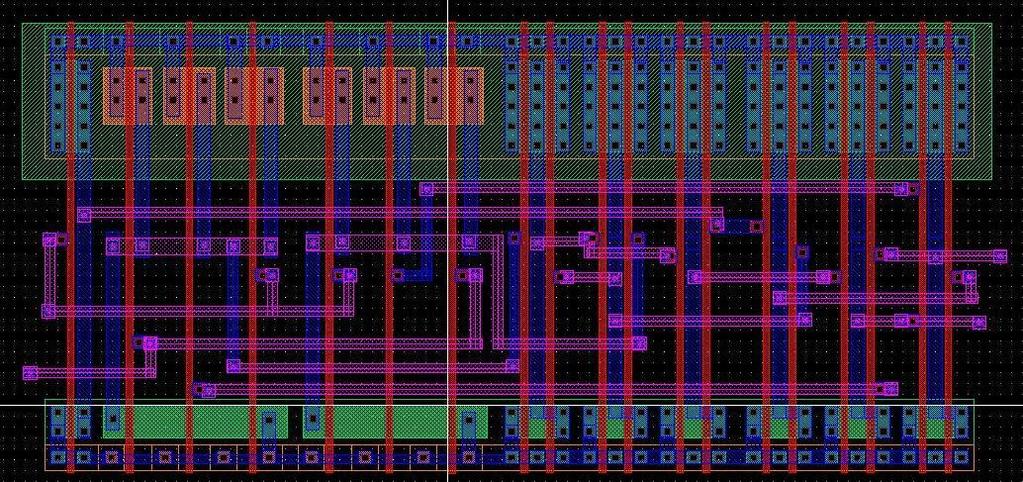
11 VII. Complete Layout of counter design: Maximum effort was made to minimize the design area on chip. Four J K flip flop was stacked on top of each other retaining minimum distance from n-well. Layout blocks are rotated to minimize interconnect requirement. AND gates used at input of each flip flop is placed at closest proximity to the J-K input and Q n and Q n output. Two bus of metal1 is used for supplying set and reset to each block. The complete layout occupies an area = 282.9µm x µm = 39,252 Figure 10: Layout of 4-bit up counter

12 Extracted Layout: Figure 11: Extracted layout of 4-bit up counter


13 Extracted layout with pad frame: Figure 12: Extracted layout including padframe VIII. Pre-layout simulation output: Figure 13: Prelayout simulation output, clock frequency= 10MHz


14 Post layout simulation output: Figure 14: Post layout simulation output, clock frequency= 10MHz Post layout simulation with capacitive load= 5pF Figure 15: Post layout simulation output, clock frequency= 10MHz, C_load= 5 pf


15 Post layout simulation with set enabled: Figure 16: Post layout simulation output with set enabled, clock frequency= 10MHz Post layout simulation output with reset enabled: Figure 17: Post layout simulation output with reset enabled, clock frequency= 10MHz
16 IX. Measurement of rise time and fall time and propagation delay: Capacitive loading was varied from 1pF to 15pF and rise time, fall time and propagation delay was measured. During rise time and fall time measurement time required to change from 30% to 70% of maximum voltage was measured. To measure propagation delay following equation was used t delay = (t PLH +t PHL )/2 Time measurement were taken for all four output bits. Q3 Load Rise (ns) Fall (ns) Delay (ns) 1pF pF pF pF pF pF pF Q2 Load Rise (ns) Fall (ns) Delay (ns) 1pF pF pF pF pF pF pF
17 Q1 Load Rise (ns) Fall (ns) Delay (ns) 1pF pF pF pF pF pF pF Q0 Load Rise (ns) Fall (ns) Delay (ns) 1pF 3pF 5pF 7pF 10pF 12pF 15pF
18 Time(ns) Time (ns) Time(ns) Time (ns) Plot of response time Vs Capacitive load: Q3 R² = rise R² = fall Linear (rise) Linear (rise) Capacitive load (pf) Q2 R² = R² = rise fall Linear (fall) Linear (fall) Capacitive load (pf) Q1 R² = R² = rise fall Linear (fall) Linear (fall) Capacitive load (pf) Q0 R² = R² = rise fall Linear (fall) Linear (fall) Capacitive load (pf) Figure 18: Plot of Rise time, fall time Vs Capacitive load
19 Time (ns) Capacitive load (pf) Q3 delay Q2 delay Q1 delay Q0 delay Linear (Q3 delay) Linear (Q2 delay) Linear (Q1 delay) Linear (Q0 delay) Figure 19: Plot of propagation delay Vs Capacitive load


20 Chip Test Results: Figure 20: Microphotograph of fabricated chip Figure 21: Microphotograph of fabricated design of 4-bit counter
- clock, Trace2 (green)- Q0, Trace3 (Purple) -Q1, Trace4(magenta) -Q2 Figure 23: Output of 4-bit counter at 10 KHz Clock signal.")
21 Test Result: Figure 22: Output of 4-bit counter at 10 KHz Clock signal. Trace 1(yellow)- clock, Trace2 (green)- Q0, Trace3 (Purple) -Q1, Trace4(magenta) -Q2 Figure 23: Output of 4-bit counter at 10 KHz Clock signal. Trace 1(yellow)- clock, Trace2 (green)- Q2, Trace3 (Purple) -Q3, Trace4(magenta) -Carry_out
22 Plot of measured chip data: Time -9.54E E E E E E E E E E E E E E E E E E E E E E E E E E E E E E E E E E E E E E E-04 Clock Volt Time -9.50E E E E E E E E E E E E E E E E E E E E E E E E E E E E E E E E E E E E E-04 Time Q0 Volt Q1 Volt Q2 Volt Time -9.44E E E E E E E E E E E E E E E E E E E E E E E E E E E E E E E E E-04 Q3 Volt -1.00E E E E E E E E E E+00 Time -9.38E E E E E E E E E E E E E E E E E E E E E E E E E E E E E E-04 Carry_out Volt
23 Discussion: Above plots show that the rise time, fall time and delay linearly varies with the capacitive loading. This indicates the liner behavior of the designed circuit. It may be noticed that the fall time higher than that of the fall time. This is because during fall time the capacitive loads discharges through the NMOS to reach ground potential. In this design a large number of NAND gates are used which has number of NMOS in series. The series connected NMOS has a larger resistance and has greater RC delay which leads to the higher value of fall time. Since in NAND gates PMOS are connected in parallel they quickly charge the load capacitor and give lower rise time. All rise time and fall time was measured for 10MHz clock frequency. At this frequency capacitive loading beyond 15pF produces signal that cannot be recognized as 1 or 0. At lower clock frequency higher capacitive loading is possible. X. Application: Counter is used widely in number of digital and analog circuit. There are vast application of counter in the field of electronics. Some of them are listed below- I. A counter can be used as frequency divider. This 4-bit counter can be efficiently used to get four different frequencies up to one sixteenth times of the original clock frequency. Since it is triggered only at negative edge of the clock, the first cycle gives output at half the frequency of that of the clock. II. Counter can be used on building entrances to keep track of number of people entering or leaving. III. Counter can be used in digital logic deigns to perform certain operation at certain steps. IV. Counters are also applicable in timer circuit to turn on/ off a device after certain time with use of a proper logic function.
24 ABSTRACT: REPORT-II For the final project in ECE-533 we had to design a four bit counter. This project was done with the aid of Cadence, in the AMI-0.6 micron process. The project involved the design of the schematic as well as the layout. In both cases, simulations were done. The counter is simulated under no-load condition as well as with few test loads. The rise time, fall time and delay are measured. I designed an Asynchronous four bit counter using T flip flops. INTRODUCTION: A Flip-flop is the name given to two-state devices which offer basic memory for sequential logic operations. Flip-flops are synchronous bistable devices that operate as memory elements. A flip-flop circuit contains two outputs, one is for the normal value and the other is for the complement value of the stored bit. Flip-flops are used for digital data storage and transfer and are commonly used in banks called "registers" for the storage of binary numerical data. Counters are designed using flip-flops. Counters can be classified as synchronous and asynchronous counters based on the application of clock to the flip-flops. A synchronous counter is clocked by a single clock for all the stages and the output for each stage changes at the same time. In an asynchronous counter the output from the previous stage is given as the clock for the next stage so that the output ripples across each stage to reach the final count. The following were the steps involved in designing this project: 1. Design a flip flop using nand gates and an inverter. 2. Draw the schematic and layout using cadence 3. Design a four bit counter using the designed flip flop 4. Draw the schematic and layout of the counter using cadence 5. Measure the rise time and fall time of the various bits 6. Measure the propagation delay across various stages with different capacitive loads
25 I have designed a four bit asynchronous counter with the aid of T flip-flops. This counter was designed to provide an output that is free of glitches. T FLIP FLOP: a) Introduction The T or "toggle" flip flop changes its output on each clock edge, giving an output which is half the frequency of the signal to the T input. T flip flop is useful for constructing binary counters, frequency dividers, and general binary addition devices. A T flip flop can be designed from a J K flip flop by shorting the J and K inputs.
26 Diagram of a T flip-flop Transition table of T Flip Flop b) Implementation : The implementation of the flip flop consists of the following steps: Designing the schematic Performing pre layout simulations Designing the layout
27 Obtaining the extracted view Performing LVS Performing post layout simulations

28 SCHEMATIC OF T FLIP FLOP: PRELAYOUT SIMULATION RESULTS:

29 LAYOUT OF T FLIP FLOP:

30 POST LAYOUT SIMULATION RESULTS: COUNTER USING T FLIP FLOPS: a) Introduction: The counter was built with the help of T-Flip Flops. The gates used in realizing the design were two 3 Input Nand Gates, three 2 Input Nand gates and an inverter. The outputs of the Flip Flop are Q and QOb. In an asynchronous counter the clock pulse is applied only at the first stage. The rest of the stages are driven by the output of the preceding flip flop. All the output bits do not change at the same time.
31 An asynchronous counter is also called as a ripple counter because only the first bit changes with the clock pulse, there exists some delay before the other bits change, so the output ripples across the counter. A binary counter can be realized using T-Flip Flops by counting the number of toggles in the previous stage. The T input of each flip-flop is set to 1 to produce a toggle at each cycle of the clock input. For each two toggles of the first cell, a toggle is produced in the second cell, and so on down to the fourth cell. This produces a binary number equal to the number of cycles of the input clock signal. Using a Master-slave configuration isolates the output from any glitches resulting from any changes happening in the input signal. The master-slave flip-flop is essentially two back-to-back JK flip-flops, but the feedback is to both to the master flip flop and the slave flip flop. In this configuration, the master flip flop sees the input when the clock is high and the output of the first stage holds the input for the next stage. During the clock low, the slave circuit is enabled to track the change in the input by using the output of the master Flip Flop. Thus the master-slave configuration eliminates any sharp change of state within a clock cycle and the flip flop is free of oscillations.
32 b) Implementation: SCHEMATIC DIAGRAM OF A 4 BIT COUNTER USING T FLIP FLOPS: PRELAYOUT SIMULATION RESULTS:
33 LAYOUT OF 4-BIT COUNTER:
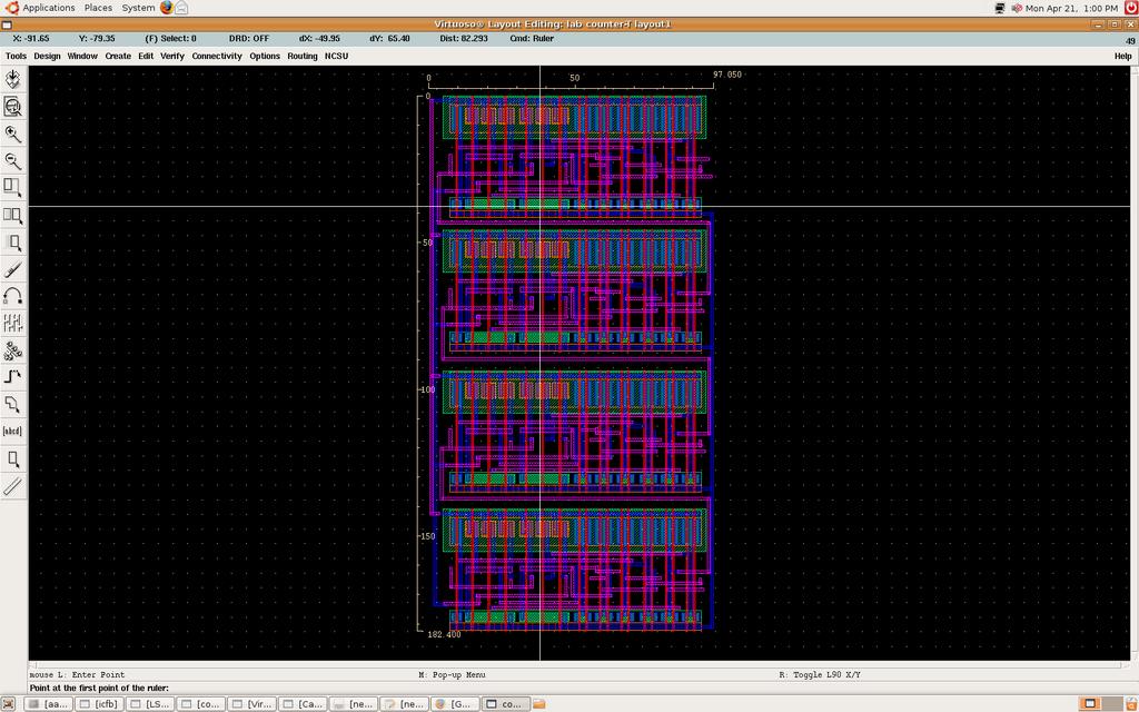
34
35
36 EXTRACTED VIEW OF THE COUNTER:

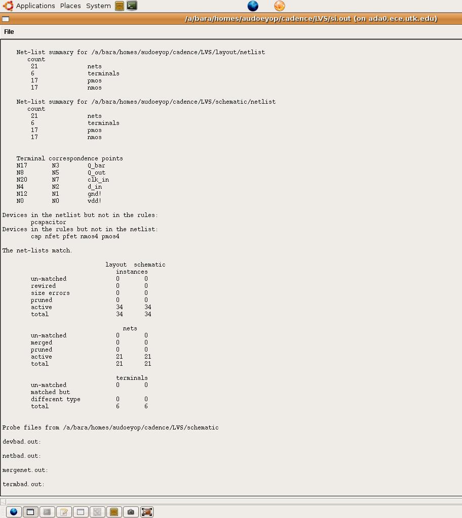
37 LAYOUT VS SCHEMATIC (LVS):
38 POST-LAYOUT SIMULATION RESULTS: RISE TIME AND FALL TIME FOR VARIOUS OUTPUT BITS AT ZERO LOAD: RISE TIME (ns) FALL TIME (ns)
39 X X X X LOAD CAPACITANCE VS PROPAGATION DELAY: X0
40 APPLICATIONS OF COUNTERS: To count the number of times that a certain event takes place. To control a fixed sequence of actions in a digital system To generate timing signals. To generate clocks of different frequencies Used in various devices such as ATM s, Watches etc SCHEMATIC OF A T FLIP FLOP:
41

42 SIMULATION RESULT OF THE T FLIP FLOP SCHEMATIC:
43 SCHEMATIC DIAGRAM OF A 4 BIT COUNTER USING T FLIP FLOPS: SIMULATION RESULT OF THE COUNTER S SCHEMATIC:
44
45 RISE TIME (ns) X FALL TIME (ns) X X X
46 Flip-Flop Design 1. Objective The objective of this project is to design and simulate a J-K Flip-Flop and a D-Flip Flop using Cadence (IC design software). The design will be in the form of a logic circuit and a layout. 2. Flip Flops 2.1 J-K Flip Flop I will be designing a J-K flip flop with a set/reset option. The outputs will only change state on the falling edge of the CLK signal, and the J and K inputs will control the future output. If both the J and K inputs are held at logic 1 and the CLK signal continues to change, the Q and Q' outputs will simply change state with each falling edge of the CLK signal. R J K Q n Q n nq 1 d d 0 Table 1: Truth Table for the J-K Flip-flop with Set/Reset 2.2 D Flip Flop I also will be designing a negative edge triggered D Flip-Flop. The outputs states to change only when the clock signal falls from logic 1 to logic 0.
47 D Q CLK Q next 0 X Falling 0 1 X Falling 1 X either logic 1 or logic 0 Table 2: Truth Table for the negative edge triggered D Flip-flop 3. Design Implementation and Simulation I designed the J-K Flip Flop and the D Flip-Flop using Cadence IC Design Software with an AMI-0.6 micron process. Ln=Lp=0.6um Wp=7.5um Wn=3.0um 3.1 Schematic Design The design process began with the schematics of the J-K flip flop (Figure 1) and the D flip flop (Figure 2), which I utilized nand gates and an inverter that I designed in my previous labs. 3.2 Schematic Simulation After designing the schematics, I simulated using Spectre and the Cadence Analog Environment in order to generate waveforms that demonstrate the behavior of the J-K flip flop (Figure 3) and the D flip flop (Figure 4). In order to simulate realistic results, capacitances were added to the outputs in order to generate delays in the waveforms. 3.2 Create Symbol
48 Symbol creation was achieved by creating symbol cell view from schematic cell view 3.3 Layout Design I then designed the layouts for the J-K flip flop (Figure5) and the D flip flop (Figure6) in which I utilized the layouts of nand gates and an inverter which I designed in my previous labs. After connecting all of the I/O pins, I made sure that I connected all of the vdd pins from each nand gate and inverter. I did the same for all of the ground (gnd) pins. 3.4 DRC Verify After the design is complete, I used the DRC tool to verify that the layouts of the J-K flip flop and the D flip flop contained no. The DRC tool confirmed that the spacing between the various components in the layouts was not too close together and that pins were not duplicated on the same layout. 3.5 Extract I created an extracted view of the layouts in which I utilized parasitic capacitances. 3.6 Verify LVS I then utilized the LVS tool to verify that the layouts designs matched that of my schematics in terms of the number of nets, terminals, and instances (Figure 7 and Figure 8). 3.7 Extracted Layout Simulation The simulation of the layouts is implemented exactly the same way as the schematic simulation. We also add capacitances to the outputs in the netlist to simulate delays and produce more realistic results. (Figure 9 and Figure 10) 4. Waveform Analysis
49 4.1 Results JK Flip Flop Simulation Waveform Figure 9 D Flip Flop Simulation Waveform Figure Rise Time, Fall Time, and Propagation Delay The rise time/fall time were measured using the 10% - 90% method. The propagation delay was measured using the 50% - 50 % method. 4.3 Capacitive Load Effect Chart Capacitive Rise Time (ns) Fall Time (ns) Propagation Delay (ns) Load (ff) Table 1: Rise time, fall time, and propagation delay measured from the J-K flip flop waveform
 Delay Time With Laod 120 100 80 60 Series1 Linear (Series1) 40 20 0 0 0.5 1 1.5 2 2.5 3 3.")
50 Capacitance (ff Capacitance (ff 4.4 Capacitive Load Effect Graphs Rise Time With Load Time (ns) Delay Time With Laod Series1 Linear (Series1) Time (ns)
51 5. Conclusion from Waveform Analysis The capacitive load and the rise/fall times and delay correlate in a linear fashion. Based on the analysis of the rise/fall times and delay we see that if the capacitive load increases, then the rise time, fall time, and delay also increase. 6. Application J-K flip flops can be utilized in binary counters, shift registers, and sequence detectors. Because of the behavior of the D-Flip Flop described in the introduction, it can be utilized in shift registers, which are an essential part of many electronic devices. 7. Pad Frame Pad frame Schematic (Figure 11) No Errors Pad frame Layout (Figure 12) DRC Clean The pad frame schematic and the pad frame layout contained no errors. However, the symbol of the JK flip flop and contained no vdd or ground pins, therefore my attempts to verify both pad frames using LVS was unsuccessful.
52 8. Appendix Figure1: J-K Flip Flop Schematic Figure 2: D Flip Flop Schematic

53 Figure 3: J-K Flip Flop Schematic Simulated Waveform


54 Figure 4: Figure 3: D Flip Flop Schematic Simulated Waveform Figure 5: J-K Flip Flop Layout Figure 6: D Flip Flop Layout

55 Figure 7: J-K Flip Flop LVS Verification
56 Figure 8: D Flip Flop LVS Verification Figure 9: J-K Flip Flop Layout Simulated Waveform


57 Figure 10: D Flip Flop Layout Simulated Waveform

58 Figure 11 JK Flip Flop Pad Frame Schematic


59 Figure 12 JK Flip Flop Pad Frame Layout
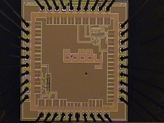
60 Microphotograph of the Chip:
Design and Simulation of a Digital CMOS Synchronous 4-bit Up-Counter with Set and Reset
 Design and Simulation of a Digital CMOS Synchronous 4-bit Up-Counter with Set and Reset Course Number: ECE 533 Spring 2013 University of Tennessee Knoxville Instructor: Dr. Syed Kamrul Islam Prepared by
Electrical & Computer Engineering ECE 491. Introduction to VLSI. Report 1
 Electrical & Computer Engineering ECE 491 Introduction to VLSI Report 1 Marva` Morrow INTRODUCTION Flip-flops are synchronous bistable devices (multivibrator) that operate as memory elements. A bistable
EL302 DIGITAL INTEGRATED CIRCUITS LAB #3 CMOS EDGE TRIGGERED D FLIP-FLOP. Due İLKER KALYONCU, 10043
 EL302 DIGITAL INTEGRATED CIRCUITS LAB #3 CMOS EDGE TRIGGERED D FLIP-FLOP Due 16.05. İLKER KALYONCU, 10043 1. INTRODUCTION: In this project we are going to design a CMOS positive edge triggered master-slave
YEDITEPE UNIVERSITY DEPARTMENT OF COMPUTER ENGINEERING. EXPERIMENT VIII: FLIP-FLOPS, COUNTERS 2014 Fall
 YEDITEPE UNIVERSITY DEPARTMENT OF COMPUTER ENGINEERING EXPERIMENT VIII: FLIP-FLOPS, COUNTERS 2014 Fall Objective: - Dealing with the operation of simple sequential devices. Learning invalid condition in
Asynchronous (Ripple) Counters
 Counters") Circuits for counting events are frequently used in computers and other digital systems. Since a counter circuit must remember its past states, it has to possess memory. The chapter about flip-flops introduced
Circuits for counting events are frequently used in computers and other digital systems. Since a counter circuit must remember its past states, it has to possess memory. The chapter about flip-flops introduced
ELEC 4609 IC DESIGN TERM PROJECT: DYNAMIC PRSG v1.2
 ELEC 4609 IC DESIGN TERM PROJECT: DYNAMIC PRSG v1.2 The goal of this project is to design a chip that could control a bicycle taillight to produce an apparently random flash sequence. The chip should operate
Experiment 8 Introduction to Latches and Flip-Flops and registers
 Experiment 8 Introduction to Latches and Flip-Flops and registers Introduction: The logic circuits that have been used until now were combinational logic circuits since the output of the device depends
Digital Logic Design Sequential Circuits. Dr. Basem ElHalawany
 Digital Logic Design Sequential Circuits Dr. Basem ElHalawany Combinational vs Sequential inputs X Combinational Circuits outputs Z A combinational circuit: At any time, outputs depends only on inputs
RS flip-flop using NOR gate
 RS flip-flop using NOR gate Triggering and triggering methods Triggering : Applying train of pulses, to set or reset the memory cell is known as Triggering. Triggering methods:- There are basically two
SEQUENTIAL LOGIC. Satish Chandra Assistant Professor Department of Physics P P N College, Kanpur
 SEQUENTIAL LOGIC Satish Chandra Assistant Professor Department of Physics P P N College, Kanpur www.satish0402.weebly.com OSCILLATORS Oscillators is an amplifier which derives its input from output. Oscillators
Introduction. NAND Gate Latch. Digital Logic Design 1 FLIP-FLOP. Digital Logic Design 1
 2007 Introduction BK TP.HCM FLIP-FLOP So far we have seen Combinational Logic The output(s) depends only on the current values of the input variables Here we will look at Sequential Logic circuits The
EMT 125 Digital Electronic Principles I CHAPTER 6 : FLIP-FLOP
 EMT 125 Digital Electronic Principles I CHAPTER 6 : FLIP-FLOP 1 Chapter Overview Latches Gated Latches Edge-triggered flip-flops Master-slave flip-flops Flip-flop operating characteristics Flip-flop applications
Chapter 4. Logic Design
 Chapter 4 Logic Design 4.1 Introduction. In previous Chapter we studied gates and combinational circuits, which made by gates (AND, OR, NOT etc.). That can be represented by circuit diagram, truth table
Chapter 6. Flip-Flops and Simple Flip-Flop Applications
 Chapter 6 Flip-Flops and Simple Flip-Flop Applications Basic bistable element It is a circuit having two stable conditions (states). It can be used to store binary symbols. J. C. Huang, 2004 Digital Logic
CS/EE 6710 Digital VLSI Design CAD Assignment #3 Due Thursday September 21 st, 5:00pm
 CS/EE 6710 Digital VLSI Design CAD Assignment #3 Due Thursday September 21 st, 5:00pm Overview: In this assignment you will design a register cell. This cell should be a single-bit edge-triggered D-type
Combinational vs Sequential
 Combinational vs Sequential inputs X Combinational Circuits outputs Z A combinational circuit: At any time, outputs depends only on inputs Changing inputs changes outputs No regard for previous inputs
ELCT201: DIGITAL LOGIC DESIGN
 ELCT201: DIGITAL LOGIC DESIGN Dr. Eng. Haitham Omran, haitham.omran@guc.edu.eg Dr. Eng. Wassim Alexan, wassim.joseph@guc.edu.eg Lecture 6 Following the slides of Dr. Ahmed H. Madian ذو الحجة 1438 ه Winter
D Latch (Transparent Latch)
") D Latch (Transparent Latch) -One way to eliminate the undesirable condition of the indeterminate state in the SR latch is to ensure that inputs S and R are never equal to 1 at the same time. This is done
D Latch (Transparent Latch) -One way to eliminate the undesirable condition of the indeterminate state in the SR latch is to ensure that inputs S and R are never equal to 1 at the same time. This is done
Chapter 5 Flip-Flops and Related Devices
 Chapter 5 Flip-Flops and Related Devices Chapter 5 Objectives Selected areas covered in this chapter: Constructing/analyzing operation of latch flip-flops made from NAND or NOR gates. Differences of synchronous/asynchronous
ECE 341. Lecture # 2
 ECE 341 Lecture # 2 Instructor: Zeshan Chishti zeshan@pdx.edu October 1, 2014 Portland State University Announcements Course website reminder: http://www.ece.pdx.edu/~zeshan/ece341.htm Homework 1: Will
Flip-Flops. Because of this the state of the latch may keep changing in circuits with feedback as long as the clock pulse remains active.
 Flip-Flops Objectives The objectives of this lesson are to study: 1. Latches versus Flip-Flops 2. Master-Slave Flip-Flops 3. Timing Analysis of Master-Slave Flip-Flops 4. Different Types of Master-Slave
Digital Fundamentals: A Systems Approach
 Digital Fundamentals: A Systems Approach Latches, Flip-Flops, and Timers Chapter 6 Traffic Signal Control Traffic Signal Control: State Diagram Traffic Signal Control: Block Diagram Traffic Signal Control:
Logic Gates, Timers, Flip-Flops & Counters. Subhasish Chandra Assistant Professor Department of Physics Institute of Forensic Science, Nagpur
 Logic Gates, Timers, Flip-Flops & Counters Subhasish Chandra Assistant Professor Department of Physics Institute of Forensic Science, Nagpur Logic Gates Transistor NOT Gate Let I C be the collector current.
COE 202: Digital Logic Design Sequential Circuits Part 1. Dr. Ahmad Almulhem ahmadsm AT kfupm Phone: Office:
 COE 202: Digital Logic Design Sequential Circuits Part 1 Dr. Ahmad Almulhem Email: ahmadsm AT kfupm Phone: 860-7554 Office: 22-324 Objectives Sequential Circuits Memory Elements Latches Flip-Flops Combinational
UNIT-3: SEQUENTIAL LOGIC CIRCUITS
 UNIT-3: SEQUENTIAL LOGIC CIRCUITS STRUCTURE 3. Objectives 3. Introduction 3.2 Sequential Logic Circuits 3.2. NAND Latch 3.2.2 RS Flip-Flop 3.2.3 D Flip-Flop 3.2.4 JK Flip-Flop 3.2.5 Edge Triggered RS Flip-Flop
RS flip-flop using NOR gate
 RS flip-flop using NOR gate Triggering and triggering methods Triggering : Applying train of pulses, to set or reset the memory cell is known as Triggering. Triggering methods:- There are basically two
Counter dan Register
 Counter dan Register Introduction Circuits for counting events are frequently used in computers and other digital systems. Since a counter circuit must remember its past states, it has to possess memory.
IT T35 Digital system desigm y - ii /s - iii
 UNIT - III Sequential Logic I Sequential circuits: latches flip flops analysis of clocked sequential circuits state reduction and assignments Registers and Counters: Registers shift registers ripple counters
LATCHES & FLIP-FLOP. Chapter 7
 LATCHES & FLIP-FLOP Chapter 7 INTRODUCTION Latch and flip flops are categorized as bistable devices which have two stable states,called SET and RESET. They can retain either of this states indefinitely
EEE2135 Digital Logic Design Chapter 6. Latches/Flip-Flops and Registers/Counters 서강대학교 전자공학과
 EEE235 Digital Logic Design Chapter 6. Latches/Flip-Flops and Registers/Counters 서강대학교 전자공학과 . Delay and Latches ) Signal Storage a. as voltage level static memory b. as charges dynamic memory 2) Delays
Counters
 Counters A counter is the most versatile and useful subsystems in the digital system. A counter driven by a clock can be used to count the number of clock cycles. Since clock pulses occur at known intervals,
Logic and Computer Design Fundamentals. Chapter 7. Registers and Counters
 Logic and Computer Design Fundamentals Chapter 7 Registers and Counters Registers Register a collection of binary storage elements In theory, a register is sequential logic which can be defined by a state
ASYNCHRONOUS COUNTER CIRCUITS
 ASYNCHRONOUS COUNTER CIRCUITS Asynchronous counters do not have a common clock that controls all the Hipflop stages. The control clock is input into the first stage, or the LSB stage of the counter. The
Design of a Low Power Four-Bit Binary Counter Using Enhancement Type Mosfet
 Design of a Low Power Four-Bit Binary Counter Using Enhancement Type Mosfet Praween Sinha Department of Electronics & Communication Engineering Maharaja Agrasen Institute Of Technology, Rohini sector -22,
Sequential Logic. E&CE 223 Digital Circuits and Systems (A. Kennings) Page 1
 Page 1") Sequential Logic E&CE 223 igital Circuits and Systems (A. Kennings) Page 1 Sequential Circuits Have considered only combinational circuits in which circuit outputs are determined entirely by current circuit
Sequential Logic E&CE 223 igital Circuits and Systems (A. Kennings) Page 1 Sequential Circuits Have considered only combinational circuits in which circuit outputs are determined entirely by current circuit
NH 67, Karur Trichy Highways, Puliyur C.F, Karur District UNIT-III SEQUENTIAL CIRCUITS
 NH 67, Karur Trichy Highways, Puliyur C.F, 639 114 Karur District DEPARTMENT OF ELETRONICS AND COMMUNICATION ENGINEERING COURSE NOTES SUBJECT: DIGITAL ELECTRONICS CLASS: II YEAR ECE SUBJECT CODE: EC2203
Chapter 7 Counters and Registers
 Chapter 7 Counters and Registers Chapter 7 Objectives Selected areas covered in this chapter: Operation & characteristics of synchronous and asynchronous counters. Analyzing and evaluating various types
Module -5 Sequential Logic Design
 Module -5 Sequential Logic Design 5.1. Motivation: In digital circuit theory, sequential logic is a type of logic circuit whose output depends not only on the present value of its input signals but on
Unit 11. Latches and Flip-Flops
 Unit 11 Latches and Flip-Flops 1 Combinational Circuits A combinational circuit consists of logic gates whose outputs, at any time, are determined by combining the values of the inputs. For n input variables,
(CSC-3501) Lecture 7 (07 Feb 2008) Seung-Jong Park (Jay) CSC S.J. Park. Announcement
 Lecture 7 (07 Feb 2008) Seung-Jong Park (Jay) CSC S.J. Park. Announcement") Seung-Jong Park (Jay) http://www.csc.lsu.edu/~sjpark Computer Architecture (CSC-3501) Lecture 7 (07 Feb 2008) 1 Announcement 2 1 Combinational vs. Sequential Logic Combinational Logic Memoryless Outputs
Seung-Jong Park (Jay) http://www.csc.lsu.edu/~sjpark Computer Architecture (CSC-3501) Lecture 7 (07 Feb 2008) 1 Announcement 2 1 Combinational vs. Sequential Logic Combinational Logic Memoryless Outputs
CHAPTER 6 COUNTERS & REGISTERS
 CHAPTER 6 COUNTERS & REGISTERS 6.1 Asynchronous Counter 6.2 Synchronous Counter 6.3 State Machine 6.4 Basic Shift Register 6.5 Serial In/Serial Out Shift Register 6.6 Serial In/Parallel Out Shift Register
Name Of The Experiment: Sequential circuit design Latch, Flip-flop and Registers
 EEE 304 Experiment No. 07 Name Of The Experiment: Sequential circuit design Latch, Flip-flop and Registers Important: Submit your Prelab at the beginning of the lab. Prelab 1: Construct a S-R Latch and
Chapter 5 Synchronous Sequential Logic
 Chapter 5 Synchronous Sequential Logic Chih-Tsun Huang ( 黃稚存 ) http://nthucad.cs.nthu.edu.tw/~cthuang/ Department of Computer Science National Tsing Hua University Outline Introduction Storage Elements:
Rangkaian Sekuensial. Flip-flop
 Rangkaian Sekuensial Rangkaian Sekuensial Flip-flop Combinational versus Sequential Functions Logic functions are categorized as being either combinational (sometimes referred to as combinatorial) or sequential.
CHAPTER 1 LATCHES & FLIP-FLOPS
 CHAPTER 1 LATCHES & FLIP-FLOPS 1 Outcome After learning this chapter, student should be able to; Recognize the difference between latches and flipflops Analyze the operation of the flip flop Draw the output
Switching Theory And Logic Design UNIT-IV SEQUENTIAL LOGIC CIRCUITS
 Switching Theory And Logic Design UNIT-IV SEQUENTIAL LOGIC CIRCUITS Sequential circuits Classification of sequential circuits: Sequential circuits may be classified as two types. 1. Synchronous sequential
A NOVEL DESIGN OF COUNTER USING TSPC D FLIP-FLOP FOR HIGH PERFORMANCE AND LOW POWER VLSI DESIGN APPLICATIONS USING 45NM CMOS TECHNOLOGY
 A NOVEL DESIGN OF COUNTER USING TSPC D FLIP-FLOP FOR HIGH PERFORMANCE AND LOW POWER VLSI DESIGN APPLICATIONS USING 45NM CMOS TECHNOLOGY Ms. Chaitali V. Matey 1, Ms. Shraddha K. Mendhe 2, Mr. Sandip A.
Flip Flop. S-R Flip Flop. Sequential Circuits. Block diagram. Prepared by:- Anwar Bari
 Sequential Circuits The combinational circuit does not use any memory. Hence the previous state of input does not have any effect on the present state of the circuit. But sequential circuit has memory
Sequential Digital Design. Laboratory Manual. Experiment #7. Counters
 The Islamic University of Gaza Engineering Faculty Department of Computer Engineering Spring 2018 ECOM 2022 Khaleel I. Shaheen Sequential Digital Design Laboratory Manual Experiment #7 Counters Objectives
DIGITAL SYSTEM FUNDAMENTALS (ECE421) DIGITAL ELECTRONICS FUNDAMENTAL (ECE422) LATCHES and FLIP-FLOPS
 DIGITAL ELECTRONICS FUNDAMENTAL (ECE422) LATCHES and FLIP-FLOPS") COURSE / CODE DIGITAL SYSTEM FUNDAMENTALS (ECE421) DIGITAL ELECTRONICS FUNDAMENTAL (ECE422) LATCHES and FLIP-FLOPS In the same way that logic gates are the building blocks of combinatorial circuits, latches
COURSE / CODE DIGITAL SYSTEM FUNDAMENTALS (ECE421) DIGITAL ELECTRONICS FUNDAMENTAL (ECE422) LATCHES and FLIP-FLOPS In the same way that logic gates are the building blocks of combinatorial circuits, latches
Final Exam review: chapter 4 and 5. Supplement 3 and 4
 Final Exam review: chapter 4 and 5. Supplement 3 and 4 1. A new type of synchronous flip-flop has the following characteristic table. Find the corresponding excitation table with don t cares used as much
ELE2120 Digital Circuits and Systems. Tutorial Note 7
 ELE2120 Digital Circuits and Systems Tutorial Note 7 Outline 1. Sequential Circuit 2. Gated SR Latch 3. Gated D-latch 4. Edge-Triggered D Flip-Flop 5. Asynchronous and Synchronous reset Sequential Circuit
3 Flip-Flops. The latch is a logic block that has 2 stable states (0) or (1). The RS latch can be forced to hold a 1 when the Set line is asserted.
 or (1). The RS latch can be forced to hold a 1 when the Set line is asserted.") 3 Flip-Flops Flip-flops and latches are digital memory circuits that can remain in the state in which they were set even after the input signals have been removed. This means that the circuits have a memory
3 Flip-Flops Flip-flops and latches are digital memory circuits that can remain in the state in which they were set even after the input signals have been removed. This means that the circuits have a memory
INTRODUCTION TO SEQUENTIAL CIRCUITS
 NOTE: Explanation Refer Class Notes Digital Circuits(15EECC203) INTRODUCTION TO SEQUENTIAL CIRCUITS by Nagaraj Vannal, Asst.Professor, School of Electronics Engineering, K.L.E. Technological University,
VTU NOTES QUESTION PAPERS NEWS RESULTS FORUMS Registers
 Registers Registers are a very important digital building block. A data register is used to store binary information appearing at the output of an encoding matrix.shift registers are a type of sequential
Introduction to Sequential Circuits
 Introduction to Sequential Circuits COE 202 Digital Logic Design Dr. Muhamed Mudawar King Fahd University of Petroleum and Minerals Presentation Outline Introduction to Sequential Circuits Synchronous
FLIP-FLOPS AND RELATED DEVICES
 C H A P T E R 5 FLIP-FLOPS AND RELATED DEVICES OUTLINE 5- NAND Gate Latch 5-2 NOR Gate Latch 5-3 Troubleshooting Case Study 5-4 Digital Pulses 5-5 Clock Signals and Clocked Flip-Flops 5-6 Clocked S-R Flip-Flop
Sequential Logic Circuits
 Sequential Logic Circuits By Dr. M. Hebaishy Digital Logic Design Ch- Rem.!) Types of Logic Circuits Combinational Logic Memoryless Outputs determined by current values of inputs Sequential Logic Has memory
cascading flip-flops for proper operation clock skew Hardware description languages and sequential logic
 equential logic equential circuits simple circuits with feedback latches edge-triggered flip-flops Timing methodologies cascading flip-flops for proper operation clock skew Basic registers shift registers
Chapter 5 Sequential Circuits
 Logic and Computer Design Fundamentals Chapter 5 Sequential Circuits Part 2 Sequential Circuit Design Charles Kime & Thomas Kaminski 28 Pearson Education, Inc. (Hyperlinks are active in View Show mode)
Chapter. Synchronous Sequential Circuits
 Chapter 5 Synchronous Sequential Circuits Logic Circuits- Review Logic Circuits 2 Combinational Circuits Consists of logic gates whose outputs are determined from the current combination of inputs. Performs
Scanned by CamScanner
 NAVEEN RAJA VELCHURI DSD & Digital IC Applications Example: 2-bit asynchronous up counter: The 2-bit Asynchronous counter requires two flip-flops. Both flip-flop inputs are connected to logic 1, and initially
Sequential Logic Basics
 Sequential Logic Basics Unlike Combinational Logic circuits that change state depending upon the actual signals being applied to their inputs at that time, Sequential Logic circuits have some form of inherent
1. Convert the decimal number to binary, octal, and hexadecimal.
 1. Convert the decimal number 435.64 to binary, octal, and hexadecimal. 2. Part A. Convert the circuit below into NAND gates. Insert or remove inverters as necessary. Part B. What is the propagation delay
ELCT201: DIGITAL LOGIC DESIGN
 ELCT201: DIGITAL LOGIC DESIGN Dr. Eng. Haitham Omran, haitham.omran@guc.edu.eg Dr. Eng. Wassim Alexan, wassim.joseph@guc.edu.eg Lecture 7 Following the slides of Dr. Ahmed H. Madian محرم 1439 ه Winter
UNIT III. Combinational Circuit- Block Diagram. Sequential Circuit- Block Diagram
 UNIT III INTRODUCTION In combinational logic circuits, the outputs at any instant of time depend only on the input signals present at that time. For a change in input, the output occurs immediately. Combinational
12-bit Wallace Tree Multiplier CMPEN 411 Final Report Matthew Poremba 5/1/2009
 12-bit Wallace Tree Multiplier CMPEN 411 Final Report Matthew Poremba 5/1/2009 Project Overview This project was originally titled Fast Fourier Transform Unit, but due to space and time constraints, the
55:131 Introduction to VLSI Design Project #1 -- Fall 2009 Counter built from NAND gates, timing Due Date: Friday October 9, 2009.
 55:131 Introduction to VLSI Design Project #1 -- Fall 2009 Counter built from NAND gates, timing Due Date: Friday October 9, 2009 Introduction In this project we will create a transistor-level model of
Lecture 8: Sequential Logic
 Lecture 8: Sequential Logic Last lecture discussed how we can use digital electronics to do combinatorial logic we designed circuits that gave an immediate output when presented with a given set of inputs
Experiment # 9. Clock generator circuits & Counters. Digital Design LAB
 Digital Design LAB Islamic University Gaza Engineering Faculty Department of Computer Engineering Fall 2012 ECOM 2112: Digital Design LAB Eng: Ahmed M. Ayash Experiment # 9 Clock generator circuits & Counters
MC9211 Computer Organization
 MC9211 Computer Organization Unit 2 : Combinational and Sequential Circuits Lesson2 : Sequential Circuits (KSB) (MCA) (2009-12/ODD) (2009-10/1 A&B) Coverage Lesson2 Outlines the formal procedures for the
Vignana Bharathi Institute of Technology UNIT 4 DLD
 DLD UNIT IV Synchronous Sequential Circuits, Latches, Flip-flops, analysis of clocked sequential circuits, Registers, Shift registers, Ripple counters, Synchronous counters, other counters. Asynchronous
Sequential Digital Design. Laboratory Manual. Experiment #3. Flip Flop Storage Elements
 The Islamic University of Gaza Engineering Faculty Department of Computer Engineering Spring 2018 ECOM 2022 Khaleel I. Shaheen Sequential Digital Design Laboratory Manual Experiment #3 Flip Flop Storage
Flip-Flops and Sequential Circuit Design
 Flip-Flops and Sequential Circuit Design ECE 52 Summer 29 Reading ssignment Brown and Vranesic 7 Flip-Flops, Registers, Counters and a Simple Processor 7.5 T Flip-Flop 7.5. Configurable Flip-Flops 7.6
DIGITAL SYSTEM FUNDAMENTALS (ECE421) DIGITAL ELECTRONICS FUNDAMENTAL (ECE422) COUNTERS
 DIGITAL ELECTRONICS FUNDAMENTAL (ECE422) COUNTERS") COURSE / CODE DIGITAL SYSTEM FUNDAMENTALS (ECE421) DIGITAL ELECTRONICS FUNDAMENTAL (ECE422) COUNTERS One common requirement in digital circuits is counting, both forward and backward. Digital clocks and
COURSE / CODE DIGITAL SYSTEM FUNDAMENTALS (ECE421) DIGITAL ELECTRONICS FUNDAMENTAL (ECE422) COUNTERS One common requirement in digital circuits is counting, both forward and backward. Digital clocks and
WINTER 15 EXAMINATION Model Answer
 Important Instructions to examiners: 1) The answers should be examined by key words and not as word-to-word as given in the model answer scheme. 2) The model answer and the answer written by candidate
Module for Lab #16: Basic Memory Devices
 Module for Lab #16: Basic Memory evices evision: November 14, 2004 LAB Overview This lab introduces the concept of electronic memory. Memory circuits store the voltage present on an input signal (LHV or
Logic Design. Flip Flops, Registers and Counters
 Logic Design Flip Flops, Registers and Counters Introduction Combinational circuits: value of each output depends only on the values of inputs Sequential Circuits: values of outputs depend on inputs and
Digital Design, Kyung Hee Univ. Chapter 5. Synchronous Sequential Logic
 Chapter 5. Synchronous Sequential Logic 1 5.1 Introduction Electronic products: ability to send, receive, store, retrieve, and process information in binary format Dependence on past values of inputs Sequential
CHAPTER1: Digital Logic Circuits
 CS224: Computer Organization S.KHABET CHAPTER1: Digital Logic Circuits 1 Sequential Circuits Introduction Composed of a combinational circuit to which the memory elements are connected to form a feedback
PESIT Bangalore South Campus
 SOLUTIONS TO INTERNAL ASSESSMENT TEST 3 Date : 8/11/2016 Max Marks: 40 Subject & Code : Analog and Digital Electronics (15CS32) Section: III A and B Name of faculty: Deepti.C Time : 11:30 am-1:00 pm Note:
EKT 121/4 ELEKTRONIK DIGIT 1
 EKT 2/4 ELEKTRONIK DIGIT Kolej Universiti Kejuruteraan Utara Malaysia Sequential Logic Circuits - COUNTERS - LATCHES (review) S-R R Latch S-R R Latch Active-LOW input INPUTS OUTPUTS S R Q Q COMMENTS Q
EKT 121/4 ELEKTRONIK DIGIT 1
 EKT 121/4 ELEKTRONIK DIGIT 1 Kolej Universiti Kejuruteraan Utara Malaysia Bistable Storage Devices and Related Devices Introduction Latches and flip-flops are the basic single-bit memory elements used
Digital Logic Design ENEE x. Lecture 19
 Digital Logic Design ENEE 244-010x Lecture 19 Announcements Homework 8 due on Monday, 11/23. Agenda Last time: Timing Considerations (6.3) Master-Slave Flip-Flops (6.4) This time: Edge-Triggered Flip-Flops
ESE 570 STATIC SEQUENTIAL CMOS LOGIC CELLS. Kenneth R. Laker, University of Pennsylvania, updated 25Mar15
 ESE 570 STATIC SEQUENTIAL CMOS LOGIC CELLS 1 Classes of Logic Circuits two stable op. pts. Latch level triggered. Flip-Flop edge triggered. one stable op. pt. One-shot single pulse output no stable op.
CHAPTER 4: Logic Circuits
 CHAPTER 4: Logic Circuits II. Sequential Circuits Combinational circuits o The outputs depend only on the current input values o It uses only logic gates, decoders, multiplexers, ALUs Sequential circuits
Review of digital electronics. Storage units Sequential circuits Counters Shifters
 Review of digital electronics Storage units Sequential circuits ounters Shifters ounting in Binary A counter can form the same pattern of 0 s and 1 s with logic levels. The first stage in the counter represents
CPS311 Lecture: Sequential Circuits
 CPS311 Lecture: Sequential Circuits Last revised August 4, 2015 Objectives: 1. To introduce asynchronous and synchronous flip-flops (latches and pulsetriggered, plus asynchronous preset/clear) 2. To introduce
More on Flip-Flops Digital Design and Computer Architecture: ARM Edition 2015 Chapter 3 <98> 98
 More on Flip-Flops Digital Design and Computer Architecture: ARM Edition 2015 Chapter 3 98 Review: Bit Storage SR latch S (set) Q R (reset) Level-sensitive SR latch S S1 C R R1 Q D C S R D latch Q
EE292: Fundamentals of ECE
 EE292: Fundamentals of ECE Fall 2012 TTh 10:00-11:15 SEB 1242 Lecture 23 121120 http://www.ee.unlv.edu/~b1morris/ee292/ 2 Outline Review Combinatorial Logic Sequential Logic 3 Combinatorial Logic Circuits
CHAPTER 4: Logic Circuits
 CHAPTER 4: Logic Circuits II. Sequential Circuits Combinational circuits o The outputs depend only on the current input values o It uses only logic gates, decoders, multiplexers, ALUs Sequential circuits
Name: Date: Suggested Reading Chapter 7, Digital Systems, Principals and Applications; Tocci
 Richland College Engineering Technology Rev. 0 B. Donham Rev. 1 (7/2003) J. Horne Rev. 2 (1/2008) J. Bradbury Digital Fundamentals CETT 1425 Lab 7 Asynchronous Ripple Counters Name: Date: Objectives: To
DIGITAL CIRCUIT COMBINATORIAL LOGIC
 DIGITAL CIRCUIT COMBINATORIAL LOGIC Logic levels: one zero true false high low CMOS logic levels: 1 => 0.7 V DD 0.4 V DD = noise margin 0 =< 0.3 V DD Positive logic: high = 1 = true low = 0 = false Negative
Other Flip-Flops. Lecture 27 1
 Other Flip-Flops Other types of flip-flops can be constructed by using the D flip-flop and external logic. Two flip-flops less widely used in the design of digital systems are the JK and T flip-flops.
SEMESTER ONE EXAMINATIONS 2002
 SEMESTER ONE EXAMINATIONS 2002 EE101 Digital Electronics Solutions Question 1. An assembly line has 3 failsafe sensors and 1 emergency shutdown switch. The Line should keep moving unless any of the following
DESIGN AND IMPLEMENTATION OF SYNCHRONOUS 4-BIT UP COUNTER USING 180NM CMOS PROCESS TECHNOLOGY
 DESIGN AND IMPLEMENTATION OF SYNCHRONOUS 4-BIT UP COUNTER USING 180NM CMOS PROCESS TECHNOLOGY Yogita Hiremath 1, Akalpita L. Kulkarni 2, J. S. Baligar 3 1 PG Student, Dept. of ECE, Dr.AIT, Bangalore, Karnataka,
B. Sc. III Semester (Electronics) - ( ) Digital Electronics-II) BE-301 MODEL ANSWER (AS-2791)
 - ( ) Digital Electronics-II) BE-301 MODEL ANSWER (AS-2791)") B. Sc. III Semester (Electronics) - (2013-14) Digital Electronics-II) BE-301 MODEL ANSWER (AS-2791) Section-[A] i. (B) ii. (A) iii. (D) iv. (C) v. (C) vi. (C) vii. (D) viii. (B) Ans-(ix): In JK flip flop
B. Sc. III Semester (Electronics) - (2013-14) Digital Electronics-II) BE-301 MODEL ANSWER (AS-2791) Section-[A] i. (B) ii. (A) iii. (D) iv. (C) v. (C) vi. (C) vii. (D) viii. (B) Ans-(ix): In JK flip flop
PRE J. Figure 25.1a J-K flip-flop with Asynchronous Preset and Clear inputs
 Asynchronous Preset and Clear Inputs The S-R, J-K and D inputs are known as synchronous inputs because the outputs change when appropriate input values are applied at the inputs and a clock signal is applied
EET2411 DIGITAL ELECTRONICS
 5-8 Clocked D Flip-FlopFlop One data input. The output changes to the value of the input at either the positive going or negative going clock trigger. May be implemented with a J-K FF by tying the J input
CSE115: Digital Design Lecture 23: Latches & Flip-Flops
 Faculty of Engineering CSE115: Digital Design Lecture 23: Latches & Flip-Flops Sections 7.1-7.2 Suggested Reading A Generic Digital Processor Building Blocks for Digital Architectures INPUT - OUTPUT Interconnect: