Design and Simulation of a Digital CMOS Synchronous 4-bit Up-Counter with Set and Reset
|
|
|
- Adelia Griffin
- 6 years ago
- Views:
Transcription
1 Design and Simulation of a Digital CMOS Synchronous 4-bit Up-Counter with Set and Reset Course Number: ECE 533 Spring 2013 University of Tennessee Knoxville Instructor: Dr. Syed Kamrul Islam Prepared by Ifana Mahbub April 26, 2013

2 1. Introduction A counter is a device which stores (and sometimes displays) the number of times a particular event or process has occurred, especially in digital logic or computing. 4-bit counters are among the most basic designs of digital systems. Because of their simplicity they are also good examples for beginners to start with their digital circuit design experience. 4-bit counter has vast number of implementations. With options such as synchronous vs. asynchronous, what flip-flops topology to use and the style of counting (binary, gray-code, etc.) various counters could be designed. The counter presented in this paper is a synchronous up-counter with serial-carry output and input set and reset options. With the serial-carry output it is possible for it to be cascaded to build a counter with more than 4 bits. Synchronous and up counter means the whole design is controlled by a single clock and that the counter will only count from 0 to F and start all over again. The input set and reset pin enables the user to set the counter to all-ones and allzero state and then to start counting again. The counter reported in this paper has been realized using JK flip-flops following a master-slave approach. This is a negative edge-sensitive flip-flop. As the J-K flip-flop can easily be used for toggle operation putting both J and K input to 1, the use of it in counter design is rightly justified. The circuit has been implemented in the AMI 0.5u process where the length was 0.6 µm for each NMOS and PMOS. 2. The design A popular approach of designing a master-slave J-K flip-flop is using two 3-input NAND gates, six 2-input NAND gates and two inverters in a feedback loop. A change of state occurs when the flip-flop senses a negative edge of the clock signal. The logic diagram of this common is shown below: Figure 1 Common Logic Diagram of a J-K Flip-flop This design has been further modified by incorporating a set and reset pin at the input. This has been accomplished easily by the addition of eight extra gates (two AND, two OR gates and two Inverters) as shown in Fig. 2.

3 Figure 2 JK FF schematic 3. Logic and truth table The counter operates on the falling edge of the clock meaning the states do not change until the clock signal inputted into the first JK flip-flop goes from logic HI to logic LO. When the set and reset input S and R are at logic 0, the flip-flop operates normally; whereas the output Q is forced to 0 irrespective of the input levels at J and K when R goes to 1 and Q is forced to 1 irrespective of the input levels at J and K when S goes to 1. Therefore, the truth table of this J- K flip-flop has been changed accordingly in Table 1. Table 1 Truth table of JK flipflop with set and reset S R J K Q n Q n ~ Q n 0 1 d d d d 1 As the counter operates on the falling edge of the input clock signal, the output only changes when the CLK signal is going from 0 to 1 as illustrated in Table 2.
4 Table 2 Truth table of 4-bit counter CLK B3 B2 B1 B Schematic and layout The final schematic is shown in Fig. 3. The equivalent W/L ratio for NMOS gates is chosen to be 2.5 and that of PMOS is 5. The width of PMOS is selected to be twice the width of NMOS because it does not hinder the correct functionality of the circuit and helps keeping the total chip area low. Moreover, the performance of the circuit is highly acceptable within a wide frequency range as we see from the simulation and different performance measurements. Different gates of the JK flipflop (schematic and layout) are shown in the following figures.


5 Figure 3 Four bit counter Schematic Figure 4 Inverter Schematic and layout Figure 5 Two input AND gate Schematic and layout


6 Figure 6 Three input NAND gate Schematic and layout Figure 7 Two input NAND gate Schematic and layout Figure 8 Two input OR gate Schematic and layout The layout of the JK flip flop is shown in Fig 9.


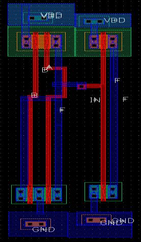
7 Figure 9 JK flip flop layout The final layout of the 4 bit counter is shown in Figure 10. Three metal layers are used to help reducing the area. The input clock signal, set and reset enter into each JK flip flop. The design on the pad frame is shown in Figure 11. As the figure shows, the dimensions of the 4-bit counter measure to be 731μm x 84μm which gives an overall area of mm2 for the design. Figure 10 Four bit counter layout
 and a closer")


8 Figure 11 Layout of 4-bit counter on pad frame (left) and a closer look (right) 5. Simulation and results Pre-Layout Simulations with set and reset pin enabled are shown in Fig 12 and 13. Figure 12 Captured pre-layout Simulation waveforms with set pin (left) and reset (right) enabled
 and set (right) pin enabled 6.")
 to 90% VDD (4.5V), and the fall time was defined as the time it took the signal to fall from 90% VDD to 10% VDD.")
9 Post-layout simulation of the design was done and the counter performed as expected. As Figure 14 shows, the counter counts up to F and then restarts back at 0. Figure 14 Captured post-layout Simulation waveforms with reset (left) and set (right) pin enabled 6. Performance analysis Table 3 depicts the rise and fall times of the counter output bits with load capacitance of 1 pf. The rise time was defined as the time it took the signal to go from 10% VDD (0.5V) to 90% VDD (4.5V), and the fall time was defined as the time it took the signal to fall from 90% VDD to 10% VDD. Table 3 Rise time and fall time for outputs with 1 pf load capacitance Output bit Rise time (ns) Fall time (ns) B B B B The rise time for each bit is less than the fall time for that bit. It means the charging RC constant is less than that of the discharging one. Figures 15 shows the delay vs. capacitance graphs of the counter output signals with load capacitances varying from 1 to 5 pf. The delay time is defined as the time it took the signal to get to 50% of VDD (2.5V) after the clock signal reached 2.5 V.
10 Delay (ns) Delay (ns) Delay (ns) Delay (ns) Cap Vs. Delay (B0) Load Capacitance (pf) Cap Vs. Delay (B2) Load Capacitance (pf) Load Capacitance (pf) Load Capacitance (pf) Figure 15 Delay vs. capacitance of the counter output signals with load capacitances varying from 1 to 5 pf From the figure we can say that the delay time for the counter increases as the load capacitance increases. 7. Test Result The chip has been tested for various frequencies. They are shown below: Cap Vs. Delay (B1) Cap Vs. Delay (B3)


11 Figure 16 Output result for input frequency of 10 KHz Figure 17 Output result for input frequency of 800 KHz Figure 18 Rise time and fall time in the edges
12 8. Conclusion This project has been a great opportunity for exercising the skills in designing digital VLSI circuits with the help of the Cadence Virtuoso Custom IC Design Tool. From various design steps of this project we have learned about many digital circuit design techniques, proper choice of transistor sizes, design rules, laying out the circuit with minimum possible area, pre and post layout simulation (with Spectre), layout extraction, LVS matching and measurement of different performance factors. This project is successful as the chip came fabricated and the proper testing has been performed.
Report on 4-bit Counter design Report- 1, 2. Report on D- Flipflop. Course project for ECE533
 Report on 4-bit Counter design Report- 1, 2. Report on D- Flipflop Course project for ECE533 I. Objective: REPORT-I The objective of this project is to design a 4-bit counter and implement it into a chip
Electrical & Computer Engineering ECE 491. Introduction to VLSI. Report 1
 Electrical & Computer Engineering ECE 491 Introduction to VLSI Report 1 Marva` Morrow INTRODUCTION Flip-flops are synchronous bistable devices (multivibrator) that operate as memory elements. A bistable
EL302 DIGITAL INTEGRATED CIRCUITS LAB #3 CMOS EDGE TRIGGERED D FLIP-FLOP. Due İLKER KALYONCU, 10043
 EL302 DIGITAL INTEGRATED CIRCUITS LAB #3 CMOS EDGE TRIGGERED D FLIP-FLOP Due 16.05. İLKER KALYONCU, 10043 1. INTRODUCTION: In this project we are going to design a CMOS positive edge triggered master-slave
YEDITEPE UNIVERSITY DEPARTMENT OF COMPUTER ENGINEERING. EXPERIMENT VIII: FLIP-FLOPS, COUNTERS 2014 Fall
 YEDITEPE UNIVERSITY DEPARTMENT OF COMPUTER ENGINEERING EXPERIMENT VIII: FLIP-FLOPS, COUNTERS 2014 Fall Objective: - Dealing with the operation of simple sequential devices. Learning invalid condition in
ELEC 4609 IC DESIGN TERM PROJECT: DYNAMIC PRSG v1.2
 ELEC 4609 IC DESIGN TERM PROJECT: DYNAMIC PRSG v1.2 The goal of this project is to design a chip that could control a bicycle taillight to produce an apparently random flash sequence. The chip should operate
CS/EE 6710 Digital VLSI Design CAD Assignment #3 Due Thursday September 21 st, 5:00pm
 CS/EE 6710 Digital VLSI Design CAD Assignment #3 Due Thursday September 21 st, 5:00pm Overview: In this assignment you will design a register cell. This cell should be a single-bit edge-triggered D-type
Asynchronous (Ripple) Counters
 Counters") Circuits for counting events are frequently used in computers and other digital systems. Since a counter circuit must remember its past states, it has to possess memory. The chapter about flip-flops introduced
Circuits for counting events are frequently used in computers and other digital systems. Since a counter circuit must remember its past states, it has to possess memory. The chapter about flip-flops introduced
(CSC-3501) Lecture 7 (07 Feb 2008) Seung-Jong Park (Jay) CSC S.J. Park. Announcement
 Lecture 7 (07 Feb 2008) Seung-Jong Park (Jay) CSC S.J. Park. Announcement") Seung-Jong Park (Jay) http://www.csc.lsu.edu/~sjpark Computer Architecture (CSC-3501) Lecture 7 (07 Feb 2008) 1 Announcement 2 1 Combinational vs. Sequential Logic Combinational Logic Memoryless Outputs
Seung-Jong Park (Jay) http://www.csc.lsu.edu/~sjpark Computer Architecture (CSC-3501) Lecture 7 (07 Feb 2008) 1 Announcement 2 1 Combinational vs. Sequential Logic Combinational Logic Memoryless Outputs
ELE2120 Digital Circuits and Systems. Tutorial Note 7
 ELE2120 Digital Circuits and Systems Tutorial Note 7 Outline 1. Sequential Circuit 2. Gated SR Latch 3. Gated D-latch 4. Edge-Triggered D Flip-Flop 5. Asynchronous and Synchronous reset Sequential Circuit
Digital Logic Design Sequential Circuits. Dr. Basem ElHalawany
 Digital Logic Design Sequential Circuits Dr. Basem ElHalawany Combinational vs Sequential inputs X Combinational Circuits outputs Z A combinational circuit: At any time, outputs depends only on inputs
RS flip-flop using NOR gate
 RS flip-flop using NOR gate Triggering and triggering methods Triggering : Applying train of pulses, to set or reset the memory cell is known as Triggering. Triggering methods:- There are basically two
DESIGN AND IMPLEMENTATION OF SYNCHRONOUS 4-BIT UP COUNTER USING 180NM CMOS PROCESS TECHNOLOGY
 DESIGN AND IMPLEMENTATION OF SYNCHRONOUS 4-BIT UP COUNTER USING 180NM CMOS PROCESS TECHNOLOGY Yogita Hiremath 1, Akalpita L. Kulkarni 2, J. S. Baligar 3 1 PG Student, Dept. of ECE, Dr.AIT, Bangalore, Karnataka,
Experiment 8 Introduction to Latches and Flip-Flops and registers
 Experiment 8 Introduction to Latches and Flip-Flops and registers Introduction: The logic circuits that have been used until now were combinational logic circuits since the output of the device depends
Counter dan Register
 Counter dan Register Introduction Circuits for counting events are frequently used in computers and other digital systems. Since a counter circuit must remember its past states, it has to possess memory.
Sequential Design Basics
 Sequential Design Basics Lecture 2 topics A review of devices that hold state A review of Latches A review of Flip-Flops Unit of text Set-Reset Latch/Flip-Flops/D latch/ Edge triggered D Flip-Flop 8/22/22
Name Of The Experiment: Sequential circuit design Latch, Flip-flop and Registers
 EEE 304 Experiment No. 07 Name Of The Experiment: Sequential circuit design Latch, Flip-flop and Registers Important: Submit your Prelab at the beginning of the lab. Prelab 1: Construct a S-R Latch and
ELCT201: DIGITAL LOGIC DESIGN
 ELCT201: DIGITAL LOGIC DESIGN Dr. Eng. Haitham Omran, haitham.omran@guc.edu.eg Dr. Eng. Wassim Alexan, wassim.joseph@guc.edu.eg Lecture 6 Following the slides of Dr. Ahmed H. Madian ذو الحجة 1438 ه Winter
Other Flip-Flops. Lecture 27 1
 Other Flip-Flops Other types of flip-flops can be constructed by using the D flip-flop and external logic. Two flip-flops less widely used in the design of digital systems are the JK and T flip-flops.
CMOS DESIGN OF FLIP-FLOP ON 120nm
 CMOS DESIGN OF FLIP-FLOP ON 120nm *Neelam Kumar, **Anjali Sharma *4 th Year Student, Department of EEE, AP Goyal Shimla University Shimla, India. neelamkumar991@gmail.com ** Assistant Professor, Department
Chapter 6. Flip-Flops and Simple Flip-Flop Applications
 Chapter 6 Flip-Flops and Simple Flip-Flop Applications Basic bistable element It is a circuit having two stable conditions (states). It can be used to store binary symbols. J. C. Huang, 2004 Digital Logic
A NOVEL DESIGN OF COUNTER USING TSPC D FLIP-FLOP FOR HIGH PERFORMANCE AND LOW POWER VLSI DESIGN APPLICATIONS USING 45NM CMOS TECHNOLOGY
 A NOVEL DESIGN OF COUNTER USING TSPC D FLIP-FLOP FOR HIGH PERFORMANCE AND LOW POWER VLSI DESIGN APPLICATIONS USING 45NM CMOS TECHNOLOGY Ms. Chaitali V. Matey 1, Ms. Shraddha K. Mendhe 2, Mr. Sandip A.
RS flip-flop using NOR gate
 RS flip-flop using NOR gate Triggering and triggering methods Triggering : Applying train of pulses, to set or reset the memory cell is known as Triggering. Triggering methods:- There are basically two
CHAPTER 1 LATCHES & FLIP-FLOPS
 CHAPTER 1 LATCHES & FLIP-FLOPS 1 Outcome After learning this chapter, student should be able to; Recognize the difference between latches and flipflops Analyze the operation of the flip flop Draw the output
COE 202: Digital Logic Design Sequential Circuits Part 1. Dr. Ahmad Almulhem ahmadsm AT kfupm Phone: Office:
 COE 202: Digital Logic Design Sequential Circuits Part 1 Dr. Ahmad Almulhem Email: ahmadsm AT kfupm Phone: 860-7554 Office: 22-324 Objectives Sequential Circuits Memory Elements Latches Flip-Flops Combinational
EMT 125 Digital Electronic Principles I CHAPTER 6 : FLIP-FLOP
 EMT 125 Digital Electronic Principles I CHAPTER 6 : FLIP-FLOP 1 Chapter Overview Latches Gated Latches Edge-triggered flip-flops Master-slave flip-flops Flip-flop operating characteristics Flip-flop applications
DIGITAL CIRCUIT COMBINATORIAL LOGIC
 DIGITAL CIRCUIT COMBINATORIAL LOGIC Logic levels: one zero true false high low CMOS logic levels: 1 => 0.7 V DD 0.4 V DD = noise margin 0 =< 0.3 V DD Positive logic: high = 1 = true low = 0 = false Negative
Sequential Digital Design. Laboratory Manual. Experiment #7. Counters
 The Islamic University of Gaza Engineering Faculty Department of Computer Engineering Spring 2018 ECOM 2022 Khaleel I. Shaheen Sequential Digital Design Laboratory Manual Experiment #7 Counters Objectives
Lecture 8: Sequential Logic
 Lecture 8: Sequential Logic Last lecture discussed how we can use digital electronics to do combinatorial logic we designed circuits that gave an immediate output when presented with a given set of inputs
Introduction. NAND Gate Latch. Digital Logic Design 1 FLIP-FLOP. Digital Logic Design 1
 2007 Introduction BK TP.HCM FLIP-FLOP So far we have seen Combinational Logic The output(s) depends only on the current values of the input variables Here we will look at Sequential Logic circuits The
1. Convert the decimal number to binary, octal, and hexadecimal.
 1. Convert the decimal number 435.64 to binary, octal, and hexadecimal. 2. Part A. Convert the circuit below into NAND gates. Insert or remove inverters as necessary. Part B. What is the propagation delay
55:131 Introduction to VLSI Design Project #1 -- Fall 2009 Counter built from NAND gates, timing Due Date: Friday October 9, 2009.
 55:131 Introduction to VLSI Design Project #1 -- Fall 2009 Counter built from NAND gates, timing Due Date: Friday October 9, 2009 Introduction In this project we will create a transistor-level model of
Parametric Optimization of Clocked Redundant Flip-Flop Using Transmission Gate
 Parametric Optimization of Clocked Redundant Flip-Flop Using Transmission Gate Sapna Sadhwani Student, Department of ECE Lakshmi Narain College of Technology Bhopal, India srsadhwani@gmail.comm Abstract
Chapter 5 Synchronous Sequential Logic
 Chapter 5 Synchronous Sequential Logic Chih-Tsun Huang ( 黃稚存 ) http://nthucad.cs.nthu.edu.tw/~cthuang/ Department of Computer Science National Tsing Hua University Outline Introduction Storage Elements:
Flip Flop. S-R Flip Flop. Sequential Circuits. Block diagram. Prepared by:- Anwar Bari
 Sequential Circuits The combinational circuit does not use any memory. Hence the previous state of input does not have any effect on the present state of the circuit. But sequential circuit has memory
Flip-Flops A) Synchronization: Clocks and Latches B) Two Stage Latch C) Memory Requires Feedback D) Simple Flip-Flop Gate
 Synchronization: Clocks and Latches B) Two Stage Latch C) Memory Requires Feedback D) Simple Flip-Flop Gate") Lecture 19: November 5, 2001 Midterm in Class Wed. Nov 7 th Covers Material 6 th -10 th week including W#10 Closed Book, Closed Notes, Bring Calculator, Paper Provided Last Name A-K 2040 Valley LSB; Last
Lecture 19: November 5, 2001 Midterm in Class Wed. Nov 7 th Covers Material 6 th -10 th week including W#10 Closed Book, Closed Notes, Bring Calculator, Paper Provided Last Name A-K 2040 Valley LSB; Last
A Power Efficient Flip Flop by using 90nm Technology
 A Power Efficient Flip Flop by using 90nm Technology Mrs. Y. Lavanya Associate Professor, ECE Department, Ramachandra College of Engineering, Eluru, W.G (Dt.), A.P, India. Email: lavanya.rcee@gmail.com
SEQUENTIAL LOGIC. Satish Chandra Assistant Professor Department of Physics P P N College, Kanpur
 SEQUENTIAL LOGIC Satish Chandra Assistant Professor Department of Physics P P N College, Kanpur www.satish0402.weebly.com OSCILLATORS Oscillators is an amplifier which derives its input from output. Oscillators
Unit 11. Latches and Flip-Flops
 Unit 11 Latches and Flip-Flops 1 Combinational Circuits A combinational circuit consists of logic gates whose outputs, at any time, are determined by combining the values of the inputs. For n input variables,
ESE 570 STATIC SEQUENTIAL CMOS LOGIC CELLS. Kenneth R. Laker, University of Pennsylvania, updated 25Mar15
 ESE 570 STATIC SEQUENTIAL CMOS LOGIC CELLS 1 Classes of Logic Circuits two stable op. pts. Latch level triggered. Flip-Flop edge triggered. one stable op. pt. One-shot single pulse output no stable op.
ELCT201: DIGITAL LOGIC DESIGN
 ELCT201: DIGITAL LOGIC DESIGN Dr. Eng. Haitham Omran, haitham.omran@guc.edu.eg Dr. Eng. Wassim Alexan, wassim.joseph@guc.edu.eg Lecture 7 Following the slides of Dr. Ahmed H. Madian محرم 1439 ه Winter
Sequential Logic. References:
 Sequential Logic Reerences: Adapted rom: Digital Integrated Circuits: A Design Perspective, J. Rabaey UCB Principles o CMOS VLSI Design: A Systems Perspective, 2nd Ed., N. H. E. Weste and K. Eshraghian
Final Exam review: chapter 4 and 5. Supplement 3 and 4
 Final Exam review: chapter 4 and 5. Supplement 3 and 4 1. A new type of synchronous flip-flop has the following characteristic table. Find the corresponding excitation table with don t cares used as much
LATCHES & FLIP-FLOP. Chapter 7
 LATCHES & FLIP-FLOP Chapter 7 INTRODUCTION Latch and flip flops are categorized as bistable devices which have two stable states,called SET and RESET. They can retain either of this states indefinitely
Chapter 2. Digital Circuits
 Chapter 2. Digital Circuits Logic gates Flip-flops FF registers IC registers Data bus Encoders/Decoders Multiplexers Troubleshooting digital circuits Most contents of this chapter were covered in 88-217
Flip-Flops and Sequential Circuit Design
 Flip-Flops and Sequential Circuit Design ECE 52 Summer 29 Reading ssignment Brown and Vranesic 7 Flip-Flops, Registers, Counters and a Simple Processor 7.5 T Flip-Flop 7.5. Configurable Flip-Flops 7.6
12-bit Wallace Tree Multiplier CMPEN 411 Final Report Matthew Poremba 5/1/2009
 12-bit Wallace Tree Multiplier CMPEN 411 Final Report Matthew Poremba 5/1/2009 Project Overview This project was originally titled Fast Fourier Transform Unit, but due to space and time constraints, the
Logic Design. Flip Flops, Registers and Counters
 Logic Design Flip Flops, Registers and Counters Introduction Combinational circuits: value of each output depends only on the values of inputs Sequential Circuits: values of outputs depend on inputs and
Chapter 5 Flip-Flops and Related Devices
 Chapter 5 Flip-Flops and Related Devices Chapter 5 Objectives Selected areas covered in this chapter: Constructing/analyzing operation of latch flip-flops made from NAND or NOR gates. Differences of synchronous/asynchronous
Design of a Low Power Four-Bit Binary Counter Using Enhancement Type Mosfet
 Design of a Low Power Four-Bit Binary Counter Using Enhancement Type Mosfet Praween Sinha Department of Electronics & Communication Engineering Maharaja Agrasen Institute Of Technology, Rohini sector -22,
Digital Fundamentals. Lab 5 Latches & Flip-Flops CETT Name: Date:
 Richland College School of Engineering & Technology Rev. 0 B. Donham Rev. 1 (7/2003) J. Horne Rev. 2 (1/2008) J. Bradbury Rev. 3 (7/2015) J. Bradbury Digital Fundamentals CETT 1425 Lab 5 Latches & Flip-Flops
Project 6: Latches and flip-flops
 Project 6: Latches and flip-flops Yuan Ze University epartment of Computer Engineering and Science Copyright by Rung-Bin Lin, 1999 All rights reserved ate out: 06/5/2003 ate due: 06/25/2003 Purpose: This
Experiment # 9. Clock generator circuits & Counters. Digital Design LAB
 Digital Design LAB Islamic University Gaza Engineering Faculty Department of Computer Engineering Fall 2012 ECOM 2112: Digital Design LAB Eng: Ahmed M. Ayash Experiment # 9 Clock generator circuits & Counters
cascading flip-flops for proper operation clock skew Hardware description languages and sequential logic
 equential logic equential circuits simple circuits with feedback latches edge-triggered flip-flops Timing methodologies cascading flip-flops for proper operation clock skew Basic registers shift registers
Chapter 4. Logic Design
 Chapter 4 Logic Design 4.1 Introduction. In previous Chapter we studied gates and combinational circuits, which made by gates (AND, OR, NOT etc.). That can be represented by circuit diagram, truth table
Sequential Digital Design. Laboratory Manual. Experiment #3. Flip Flop Storage Elements
 The Islamic University of Gaza Engineering Faculty Department of Computer Engineering Spring 2018 ECOM 2022 Khaleel I. Shaheen Sequential Digital Design Laboratory Manual Experiment #3 Flip Flop Storage
EKT 121/4 ELEKTRONIK DIGIT 1
 EKT 121/4 ELEKTRONIK DIGIT 1 Kolej Universiti Kejuruteraan Utara Malaysia Bistable Storage Devices and Related Devices Introduction Latches and flip-flops are the basic single-bit memory elements used
LFSR Counter Implementation in CMOS VLSI
 LFSR Counter Implementation in CMOS VLSI Doshi N. A., Dhobale S. B., and Kakade S. R. Abstract As chip manufacturing technology is suddenly on the threshold of major evaluation, which shrinks chip in size
CSE Latches and Flip-flops Dr. Izadi. NOR gate property: A B Z Cross coupled NOR gates: S M S R Q M
 CSE-4523 Latches and Flip-flops Dr. Izadi NOR gate property: A B Z A B Z Cross coupled NOR gates: S M S R M R S M R S R S R M S S M R R S ' Gate R Gate S R S G R S R (t+) S G R Flip_flops:. S-R flip-flop
Universal Asynchronous Receiver- Transmitter (UART)
") Universal Asynchronous Receiver- Transmitter (UART) (UART) Block Diagram Four-Bit Bidirectional Shift Register Shift Register Counters Shift registers can form useful counters by recirculating a pattern
Universal Asynchronous Receiver- Transmitter (UART) (UART) Block Diagram Four-Bit Bidirectional Shift Register Shift Register Counters Shift registers can form useful counters by recirculating a pattern
Sequential Logic. E&CE 223 Digital Circuits and Systems (A. Kennings) Page 1
 Page 1") Sequential Logic E&CE 223 igital Circuits and Systems (A. Kennings) Page 1 Sequential Circuits Have considered only combinational circuits in which circuit outputs are determined entirely by current circuit
Sequential Logic E&CE 223 igital Circuits and Systems (A. Kennings) Page 1 Sequential Circuits Have considered only combinational circuits in which circuit outputs are determined entirely by current circuit
CHAPTER 6 COUNTERS & REGISTERS
 CHAPTER 6 COUNTERS & REGISTERS 6.1 Asynchronous Counter 6.2 Synchronous Counter 6.3 State Machine 6.4 Basic Shift Register 6.5 Serial In/Serial Out Shift Register 6.6 Serial In/Parallel Out Shift Register
Counters
 Counters A counter is the most versatile and useful subsystems in the digital system. A counter driven by a clock can be used to count the number of clock cycles. Since clock pulses occur at known intervals,
Chapter 7 Counters and Registers
 Chapter 7 Counters and Registers Chapter 7 Objectives Selected areas covered in this chapter: Operation & characteristics of synchronous and asynchronous counters. Analyzing and evaluating various types
EKT 121/4 ELEKTRONIK DIGIT 1
 EKT 2/4 ELEKTRONIK DIGIT Kolej Universiti Kejuruteraan Utara Malaysia Sequential Logic Circuits - COUNTERS - LATCHES (review) S-R R Latch S-R R Latch Active-LOW input INPUTS OUTPUTS S R Q Q COMMENTS Q
Logic Circuits. A gate is a circuit element that operates on a binary signal.
 Logic Circuits gate is a circuit element that operates on a binary signal. Logic operations typically have three methods of description:. Equation symbol 2. Truth table 3. Circuit symbol The binary levels
Introduction to Sequential Circuits
 Introduction to Sequential Circuits COE 202 Digital Logic Design Dr. Muhamed Mudawar King Fahd University of Petroleum and Minerals Presentation Outline Introduction to Sequential Circuits Synchronous
CHAPTER 4: Logic Circuits
 CHAPTER 4: Logic Circuits II. Sequential Circuits Combinational circuits o The outputs depend only on the current input values o It uses only logic gates, decoders, multiplexers, ALUs Sequential circuits
Digital Circuits I and II Nov. 17, 1999
 Physics 623 Digital Circuits I and II Nov. 17, 1999 Digital Circuits I 1 Purpose To introduce the basic principles of digital circuitry. To understand the small signal response of various gates and circuits
LOW-POWER CLOCK DISTRIBUTION IN EDGE TRIGGERED FLIP-FLOP
 LOW-POWER CLOCK DISTRIBUTION IN EDGE TRIGGERED FLIP-FLOP Rahul Yadav 1, Rahul Shrivastava 2, Vijay Yadav 3 1 M.Tech Scholar, 2 Asst. Prof., 3 Asst. Prof Department of Electronics and Communication Engineering,
Digital Circuits ECS 371
 igital Circuits ECS 371 r. Prapun Suksompong prapun@siit.tu.ac.th Lecture 17 Office Hours: BK 3601-7 Monday 9:00-10:30, 1:30-3:30 Tuesday 10:30-11:30 1 Announcement Reading Assignment: Chapter 7: 7-1,
DIGITAL SYSTEM FUNDAMENTALS (ECE421) DIGITAL ELECTRONICS FUNDAMENTAL (ECE422) LATCHES and FLIP-FLOPS
 DIGITAL ELECTRONICS FUNDAMENTAL (ECE422) LATCHES and FLIP-FLOPS") COURSE / CODE DIGITAL SYSTEM FUNDAMENTALS (ECE421) DIGITAL ELECTRONICS FUNDAMENTAL (ECE422) LATCHES and FLIP-FLOPS In the same way that logic gates are the building blocks of combinatorial circuits, latches
COURSE / CODE DIGITAL SYSTEM FUNDAMENTALS (ECE421) DIGITAL ELECTRONICS FUNDAMENTAL (ECE422) LATCHES and FLIP-FLOPS In the same way that logic gates are the building blocks of combinatorial circuits, latches
SEMESTER ONE EXAMINATIONS 2002
 SEMESTER ONE EXAMINATIONS 2002 EE101 Digital Electronics Solutions Question 1. An assembly line has 3 failsafe sensors and 1 emergency shutdown switch. The Line should keep moving unless any of the following
Logic Gates, Timers, Flip-Flops & Counters. Subhasish Chandra Assistant Professor Department of Physics Institute of Forensic Science, Nagpur
 Logic Gates, Timers, Flip-Flops & Counters Subhasish Chandra Assistant Professor Department of Physics Institute of Forensic Science, Nagpur Logic Gates Transistor NOT Gate Let I C be the collector current.
Combinational vs Sequential
 Combinational vs Sequential inputs X Combinational Circuits outputs Z A combinational circuit: At any time, outputs depends only on inputs Changing inputs changes outputs No regard for previous inputs
Design of a High Frequency Dual Modulus Prescaler using Efficient TSPC Flip Flop using 180nm Technology
 Design of a High Frequency Dual Modulus Prescaler using Efficient TSPC Flip Flop using 180nm Technology Divya shree.m 1, H. Venkatesh kumar 2 PG Student, Dept. of ECE, Nagarjuna College of Engineering
IT T35 Digital system desigm y - ii /s - iii
 UNIT - III Sequential Logic I Sequential circuits: latches flip flops analysis of clocked sequential circuits state reduction and assignments Registers and Counters: Registers shift registers ripple counters
UNIT-3: SEQUENTIAL LOGIC CIRCUITS
 UNIT-3: SEQUENTIAL LOGIC CIRCUITS STRUCTURE 3. Objectives 3. Introduction 3.2 Sequential Logic Circuits 3.2. NAND Latch 3.2.2 RS Flip-Flop 3.2.3 D Flip-Flop 3.2.4 JK Flip-Flop 3.2.5 Edge Triggered RS Flip-Flop
Registers and Counters
 Registers and Counters Clocked sequential circuit = F/Fs and combinational gates Register Group of flip-flops (share a common clock and capable of storing one bit of information) Consist of a group of
CHAPTER 4: Logic Circuits
 CHAPTER 4: Logic Circuits II. Sequential Circuits Combinational circuits o The outputs depend only on the current input values o It uses only logic gates, decoders, multiplexers, ALUs Sequential circuits
DESIGN OF DOUBLE PULSE TRIGGERED FLIP-FLOP BASED ON SIGNAL FEED THROUGH SCHEME
 Scientific Journal Impact Factor (SJIF): 1.711 e-issn: 2349-9745 p-issn: 2393-8161 International Journal of Modern Trends in Engineering and Research www.ijmter.com DESIGN OF DOUBLE PULSE TRIGGERED FLIP-FLOP
ECE 263 Digital Systems, Fall 2015
 ECE 263 Digital Systems, Fall 2015 REVIEW: FINALS MEMORY ROM, PROM, EPROM, EEPROM, FLASH RAM, DRAM, SRAM Design of a memory cell 1. Draw circuits and write 2 differences and 2 similarities between DRAM
Module -5 Sequential Logic Design
 Module -5 Sequential Logic Design 5.1. Motivation: In digital circuit theory, sequential logic is a type of logic circuit whose output depends not only on the present value of its input signals but on
A Design for Improved Very Low Power Static Flip Flop Using Two Inverters and Five NORs
 A Design for Improved Very Low Power Static Flip Flop Using Two Inverters and Five NORs Jogi Prakash 1, G. Someswara Rao 2, Ganesan P 3, G. Ravi Kishore 4, Sandeep Chilumula 5 1 M Tech Student, 2, 4, 5
Digital Design, Kyung Hee Univ. Chapter 5. Synchronous Sequential Logic
 Chapter 5. Synchronous Sequential Logic 1 5.1 Introduction Electronic products: ability to send, receive, store, retrieve, and process information in binary format Dependence on past values of inputs Sequential
Logic Design Viva Question Bank Compiled By Channveer Patil
 Logic Design Viva Question Bank Compiled By Channveer Patil Title of the Practical: Verify the truth table of logic gates AND, OR, NOT, NAND and NOR gates/ Design Basic Gates Using NAND/NOR gates. Q.1
NH 67, Karur Trichy Highways, Puliyur C.F, Karur District UNIT-III SEQUENTIAL CIRCUITS
 NH 67, Karur Trichy Highways, Puliyur C.F, 639 114 Karur District DEPARTMENT OF ELETRONICS AND COMMUNICATION ENGINEERING COURSE NOTES SUBJECT: DIGITAL ELECTRONICS CLASS: II YEAR ECE SUBJECT CODE: EC2203
MAHARASHTRA STATE BOARD OF TECHNICAL EDUCATION (Autonomous)
") Subject Code: 17320 Model Answer Page 1 of 32 Important Instructions to examiners: 1) The answers should be examined by key words and not as word-to-word as given in the Model answer scheme. 2) The model
Subject Code: 17320 Model Answer Page 1 of 32 Important Instructions to examiners: 1) The answers should be examined by key words and not as word-to-word as given in the Model answer scheme. 2) The model
ECE 341. Lecture # 2
 ECE 341 Lecture # 2 Instructor: Zeshan Chishti zeshan@pdx.edu October 1, 2014 Portland State University Announcements Course website reminder: http://www.ece.pdx.edu/~zeshan/ece341.htm Homework 1: Will
ASYNCHRONOUS COUNTER CIRCUITS
 ASYNCHRONOUS COUNTER CIRCUITS Asynchronous counters do not have a common clock that controls all the Hipflop stages. The control clock is input into the first stage, or the LSB stage of the counter. The
P.Akila 1. P a g e 60
 Designing Clock System Using Power Optimization Techniques in Flipflop P.Akila 1 Assistant Professor-I 2 Department of Electronics and Communication Engineering PSR Rengasamy college of engineering for
A FOUR GAIN READOUT INTEGRATED CIRCUIT : FRIC 96_1
 A FOUR GAIN READOUT INTEGRATED CIRCUIT : FRIC 96_1 J. M. Bussat 1, G. Bohner 1, O. Rossetto 2, D. Dzahini 2, J. Lecoq 1, J. Pouxe 2, J. Colas 1, (1) L. A. P. P. Annecy-le-vieux, France (2) I. S. N. Grenoble,
3 Flip-Flops. The latch is a logic block that has 2 stable states (0) or (1). The RS latch can be forced to hold a 1 when the Set line is asserted.
 or (1). The RS latch can be forced to hold a 1 when the Set line is asserted.") 3 Flip-Flops Flip-flops and latches are digital memory circuits that can remain in the state in which they were set even after the input signals have been removed. This means that the circuits have a memory
3 Flip-Flops Flip-flops and latches are digital memory circuits that can remain in the state in which they were set even after the input signals have been removed. This means that the circuits have a memory
International Research Journal of Engineering and Technology (IRJET) e-issn: Volume: 03 Issue: 07 July p-issn:
 e-issn: Volume: 03 Issue: 07 July p-issn:") IC Layout Design of Decoder Using Electrical VLSI System Design 1.UPENDRA CHARY CHOKKELLA Assistant Professor Electronics & Communication Department, Guru Nanak Institute Of Technology-Ibrahimpatnam (TS)-India
IC Layout Design of Decoder Using Electrical VLSI System Design 1.UPENDRA CHARY CHOKKELLA Assistant Professor Electronics & Communication Department, Guru Nanak Institute Of Technology-Ibrahimpatnam (TS)-India
Section 6.8 Synthesis of Sequential Logic Page 1 of 8
 Section 6.8 Synthesis of Sequential Logic Page of 8 6.8 Synthesis of Sequential Logic Steps:. Given a description (usually in words), develop the state diagram. 2. Convert the state diagram to a next-state
Unit 9 Latches and Flip-Flops. Dept. of Electrical and Computer Eng., NCTU 1
 Unit 9 Latches and Flip-Flops Dept. of Electrical and Computer Eng., NCTU 1 9.1 Introduction Dept. of Electrical and Computer Eng., NCTU 2 What is the characteristic of sequential circuits in contrast
Switching Circuits & Logic Design
 Switching Circuits & Logic Design Jie-Hong oland Jiang 江介宏 Department of Electrical Engineering National Taiwan University Fall 22 Latches and Flip-Flops http://www3.niaid.nih.gov/topics/malaria/lifecycle.htm
L4: Sequential Building Blocks (Flip-flops, Latches and Registers)
") L4: Sequential Building Blocks (Flip-flops, Latches and Registers) Acknowledgements: Lecture material adapted from R. Katz, G. Borriello, Contemporary Logic esign (second edition), Prentice-Hall/Pearson
L4: Sequential Building Blocks (Flip-flops, Latches and Registers) Acknowledgements: Lecture material adapted from R. Katz, G. Borriello, Contemporary Logic esign (second edition), Prentice-Hall/Pearson
UNIT IV. Sequential circuit
 UNIT IV Sequential circuit Introduction In the previous session, we said that the output of a combinational circuit depends solely upon the input. The implication is that combinational circuits have no
Logic and Computer Design Fundamentals. Chapter 7. Registers and Counters
 Logic and Computer Design Fundamentals Chapter 7 Registers and Counters Registers Register a collection of binary storage elements In theory, a register is sequential logic which can be defined by a state
EET2411 DIGITAL ELECTRONICS
 5-8 Clocked D Flip-FlopFlop One data input. The output changes to the value of the input at either the positive going or negative going clock trigger. May be implemented with a J-K FF by tying the J input