Panasonic Service and Technology Company
|
|
|
- Nathan Mason
- 5 years ago
- Views:
Transcription

1 Panasonic Service and Technology Company Technical Guide 10 th Generation Plasma Display Television National Training
2 Panasonic Service and Technology Company Prepared by Cesar Perdomo and Jean Magloire Panasonic Service and Technology Company National Training Copyright 2007 by Panasonic Services Company All rights reserved. Unauthorized copying and distribution is a violation of law. Warning This service information is designed for experienced repair technicians only and is not designed for use by the general public. It does not contain warnings or cautions to advise non-technical individuals of potential dangers in attempting to service a product. Products powered by electricity should be serviced or repaired only by experienced professional technicians. Any attempt to service or repair the product or products dealt with in this service information by anyone else could result in serious injury or death.
3 Table of Contents Subject Page # Subject Page # 2007 Panasonic Plasma Line-up 5 Troubleshooting (No Power/Dead Unit) Part 2 56 Models Comparison 6 SOS Circuit Overview 59 High Resolution (FULL-HD Panel) 9 DRV_RST SOS 62 TH-42PX75U Board Layout & Description 13 Location of Q TH-42PX75U Board Layout (Pictorial) 14 Close-up View of Q /2007 Signal Process/Switching Circuit 15 5 Blinks SOS (1) 66 Overall Block Diagram 16 SOS (Drive-reset) 68 Standby Circuit 21 D & C Boards Connection 69 STB5V/STB3.3V Distribution Blinks SOS 70 Main CPU VCC Supply (A Board) 28 Signal Circuit Overview 75 TV_SUB_ON/TUNER_SUB_ON 30 Video Process Block Diagram 77 TV_SUB_ON (F_STB_ON) 32 D Board Block Diagram 79 TV_SUB_ON (Relay Drive Circuit) 34 Panel Drive (TH-42PX75U) 81 PFC Circuit 36 Audio Process Block Diagram 83 ACFB (Active Clamp Full Bridge Switching) Circuit 37 Self-Check Function 88 MAIN/SUB Voltages 39 How to Reset the Unit 89 F+15V, DTV9V, SUB5V SOS Detect Circuit 41 Self-Check Menu 90 Power On Operation 43 Check point 91 P15V/P5V Circuit 51 Serviceman Mode 92 Vsus/Vda Circuit 53 Serviceman Mode Menu and Navigation 93 Troubleshooting (No Power/Dead Unit) Part 1 55 Internal Test Patterns 95 3
4 Table of Contents (Continued) Subject Page # Driver Setup Adjustment 96 Initialization Pulse Adjustment 97 Quick adjustment after P.C.B. exchange 98 4


5 2007 Panasonic Plasma Line-up 5
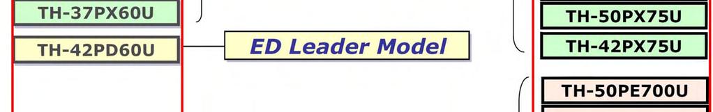
6 Models Comparison 6

7 Models Comparison 7

8 Models Comparison 8
 Full-HD PDP (approx.")
9 High Resolution (FULL-HD Panel) The Full-HD plasma panel boasts a total of about 2,070,000 pixels (1920 x 1080). It renders true-to-life HD images with about twice the resolution of a standard HD panel. HD PDP (approx. 1,050,000 pixels) Full-HD PDP (approx. 2,070,000 pixels) (Image resolution about twice as high) *When compared to the 50PX600 About Twice the Resolution of a Standard HD PDP! 9
10 10
11 10 th Generation Plasma Television Board Layout 11
12 12

13 TH-42PX75U Boards Layout & Description Panasonic started using single scan addressing in the 42 HD models last year when the 9th generation of Plasma TV was introduced. The single scan addressing was only used on standard definition models previously. For this generation, Panasonic has added the 50 models to the list of TV using single scan addressing. 13
")
14 TH-42PX75U Board Layout (Pictorial) 14

15 2006/2007 Signal Process/Switching Circuit The plasma models have less boards than the previous generation. The PA, DT, DG, H, and HC boards used on the models are now incorporated within the new A board of the 2007 models. 15
16 Overall Block Diagram 16
17 Overall Block Diagram The operation of the plasma TV can be divided into 3 different sections: 1. Power Supply Circuit The power supply circuit board (P board) provides voltages to the Signal switching/processing circuit and the Panel drive circuit. 2. Signal Switching/Processing Circuit Upon connecting the unit to the AC voltage source, the STB5V of the P board is provided to the A board for system control operation. The F_STB15V is also provided to the signal switching/processing circuit of the A board. It remains present for approximately 25 seconds unless the power button is pressed. This circuit also receives 15V for audio operation and fan drive for models with fan. 3. Panel Drive Circuit. The Panel drive circuit receives the Vsus, Vda, 15V, and 5V sources from the P board when the unit is in operation. 17
18 18
19 10 th Generation Plasma Television Power Supply 19
20 20

21 Standby Circuit 21
22 Standby Circuit 1. When the TV is connected to the AC line, the power supply outputs 5V. 2. This voltage is applied to the D board and the A board. The 5V applied to the D board in the Panel Drive Section is not used during standby operation. 3. On the other hand, when the A board receives the 5V from the Power supply, it outputs the F_STB_ON command. 4. This command is applied to the power supply board to generate the F_STB15V. The F_STB15V is applied to the A board to energize the Signal SW/Process Circuit. 22

23 Standby Circuit 23
24 Standby Circuit When AC is applied to the TV, the Standby circuit outputs 5Vdc and 12Vdc. The 5V is applied to the Power MCU and the switching transistor Q537 of the power supply circuit. The 12V is provided to the SS board. A jumper at connector SS34 of the SS board routes the 12V back into the power supply board to turn on Q537. When Q537 is on, the STB5V is output to the D and A boards. On the D board, the STB5V is applied to a 3.3V regulator (IC9011). During standby operation, this regulator is kept off to disable the panel drive circuits. The STB5V is also applied to a 3.3V regulator (IC5604) on the A board to provide the supply voltage (STB3.3V) to the Main CPU (IC1100). The STB3.3V is also applied the Remote Control receiver and the power LED on the K board. Furthermore, the STB3.3V is provided to the SD card slot (Not shown in the diagram). When the Main CPU IC1100 receives the 3.3V, it outputs the TV_SUB_ON/TUNER_SUB_ON command to the Power MCU (IC501) located on the Power Supply board. Subsequently, the power MCU outputs the following commands: 1. Relays ON/OFF _ To turn on the circuit that activates on the AC relays. The PFC (Power Factor Control) circuit goes into operation to create the DC voltage needed to power the ACFB circuit. 2. VLOW ON/OFF _ to turn on the ACFB (Active Clamp Full Bridge) circuit to generate the 15V. 3. F_STB_ON/OFF_ to provide the command to turn on the DC-DC converter to output the F+15V. The F+15V is applied to the 5V/9V regulator, IC3500, on the A board. The voltage outputs of IC3500 are used by various circuits on the A board. To avoid catastrophic failures, they are monitored by an SOS Detect circuit for over-voltage and over-current conditions. This SOS Detect circuit is controlled by the TUNER_SUB_ON command from the Main CPU (IC1100). The 9V from IC3500 is also applied to a 3.3V regulator (IC5600). The 5V and 9V from IC3500 and the 3.3V from IC5600 are connected to the CPU for voltage presence detection. 24
 to generate the STB3.3V to power the MAIN MICON Genx4 (IC1100). The STB3.3V is also connected to the remote receiver IC and the power LED on the K board.")
25 STB5V/STB3.3V Distribution The STB5V is connected to the D and A boards. During standby, this voltage is not used by the D board. On the A board, the STB5V is applied to a 3.3V regulator (IC5604) to generate the STB3.3V to power the MAIN MICON Genx4 (IC1100). The STB3.3V is also connected to the remote receiver IC and the power LED on the K board. 25
 on the D board is not active during Standby. The transistor Q9014 is on to keep PANEL_STBY_ON low.")
26 STB5V (2) P25 This circuit combined with the circuit in the following page is used to explain the reason why the CPU (IC9003) on the D board is not active during Standby. The transistor Q9014 is on to keep PANEL_STBY_ON low. 26

27 STB5V (3) The STB5V source is connected to the voltage input (pin 4) of the RESET/STB3.3V regulator IC9011. The output of this IC is controlled by the ON/OFF pin (Pin 6). The DC level of this pin is determined by the STB3.3V ON/OFF circuit. During standby pin 6 of IC9011 is low keeping IC9011 off. When the power is turned on; pin 6 goes high, the IC turns on and outputs 3.3V on pin 3. 27

28 Main CPU VCC Supply (A Board) 28
29 Main CPU VCC Supply (A Board) On the A board, the STB5V is applied to pins 3 and 4 of the 3.3V regulator (IC5604). Pin 4 is the voltage input to the IC and pin 3 is the ON/OFF command. The STB5V at pin 3 allows pin 5 to output 3.3V. The 3.3V from IC5604 is then applied to pins 31, 50, 74, 78, 81, 85, and 100 of the CPU (IC1100). This turns on the main CPU (IC1100) and a high command (TV_SUB_ON/TUNER_SUB_ON) is output on pin 1. This command splits in 2 (TUNER_SUB_ON and TV_SUB_ON). The TUNER_SUB_ON command together with the STB5V is applied to the SOS detect circuit to monitor the sub voltages generated in the A board. The TV_SUB_ON command is applied to the power supply board (P board) to create the F+15V. 29

30 TV_SUB_ON/TUNER_SUB_ON 30
31 TV_SUB_ON/TUNER_SUB_ON The STB 5V at pin 5 of connector A7 and the TV SUB ON command at pin 6 are used to activate the PA SOS detect circuit on the A board. This circuit monitors the F+15V, DT9V, and SUB5V for abnormality. Under normal operation, the TUNER_SUB_ON voltage from pin 1 of the main CPU (IC1101) turns on Q3504. When Q3504 is on, a low is applied to the base of Q3502 turning it on. When Q3502 is on, 5V is applied to the emitter and base of Q3503. The transistor remains off until a short circuit or excessive voltage is developed in the supply lines connected to its base. When Q3503 is off, a low is output to pin 114 of IC
 P")
32 TV_SUB_ON (F_STB_ON) P Board P 32
33 TV_SUB_ON (F_STB_ON) The F-STB-ON voltage (3.2V) from pin 6 of connector P7 is applied to pin 23 of the Power CPU (IC501) on the P board. IC501 sends out commands to first turn on the primary circuit of the power supply, and then the circuit that allows the F_STB15V to develop. 1. The relay commands (high) from pins 11 and 12 of IC501 are used to trigger the relays RL402 and RL A low from pin 16 of IC501 is used to turn on the power factor control IC (IC406) to generate the 395V DC. 3. A high from pin 15 of IC501 is used to turn on the V-low power control IC (IC520) to turn on the oscillator in the Active Clamp Full Bridge System circuit. 4. A low from pin 18 of IC501 is used to turn on the F_STB15V DC/DC converter Q
")
34 TV_SUB_ON (Relay Drive Circuit) 34
35 TV_SUB_ON (Relay Drive Circuit) The F_STBY_ON voltage (3.2V) from pin 6 of connector P7 is applied to pin 23 of the power MCU (IC501) on the P board. When pin 23 goes high, pin 12 goes high turning on Q502 to trigger the inrush relay RL403. Approximately 300ms later, pin 11 also goes high turning on Q501 to trigger the main relay RL ms later, pin 12 goes low allowing for only the main relay RL402 to remain on. RL401 is triggered whenever RL402 or RL403 are triggered. AC voltage flows through the relays contact, the line filter and the bridge rectifier D401 for conversion into DC. 35

36 PFC Circuit Pin 16 of IC501 also goes low when pin 23 is high. When pin 16 goes low, the diode within the photo-coupler IC401 emits light to turn on the photo-transistor. Pin 4 of IC401 goes low. This low is applied to the gate of Q401 turning it on to apply 12V to pin 8 of PFC circuit. 36
 Circuit")
37 ACFB (Active Clamp Full Bridge Switching) Circuit 37
38 ACFB (Active Clamp Full Bridge Switching) Circuit The PFC 395VDC is applied to the switching circuit (Q408, Q409, Q412, and Q413). The operation of this switching circuit is controlled by the transformer T402 which is driven by the V-low power control IC, IC A high from pin 15 of IC501 is used to turn on the power control IC (IC520) to energize the primary of transformer T402 and allow the switching circuit to drive transformer T The secondary circuit of transformer T404 outputs the Vsus, Vda, and 15V voltage sources. 3. The 15V is applied to the DC-DC converter (Q556). The output of Q556 is controlled by pin Pin 18 goes low to turn off Q524. When Q524 is off, 22V is applied to pin 4 of Q556 turning it on. At this time pins 1, 2, and 3 of Q556 output the F_STB15V. 5. The F_STB15V is applied to pins 7, 8, and 9 of connector P6. 38

39 MAIN/SUB Voltages 39
40 MAIN/SUB Voltages The F+15V from the power supply is applied to pins 6, 7, and 8 of connector A6 on the A board. The 15V is applied to the voltage input pin (pin 9) of the SUB+5V/SUB+9V dual regulator IC3500. The 15V is also used to keep pin 1 and pin 15 high. Pin 1 and pin 15 are the ON/OFF pins. When pin 1 is high, pin 3 outputs 5V. When pin 15 is high, pin 13 outputs 9V. D3500 monitors the 15V line for OVER VOLTAGE condition. If the 15V becomes excessive, D3500 conducts to turn on Q3500. When Q3500 is on, pin1 and pin 15 go low to disable IC3500. The 9V from pin 13 of IC3500 is applied to the 3.3V DC-DC converter (IC5600) to generate the SUB3.3V. The 9V is also applied to the 1.2V/1.8V DC-DC converter (IC5601) to generate the SUB1.2V and the SUB1.8V 40

41 F+15V, DTV9V, SUB5V SOS Detect Circuit 41
42 F+15V, DTV9V, SUB5V SOS Detect Circuit The F+15V, DTV9V, and SUB5V are monitored for over-voltage and over-current conditions by the SOS circuit on the A board. Under normal condition, pin 114 of the main CPU (IC1100) is low. When a short circuit or an over-voltage condition occurs, the SOS detect circuit is triggered causing pin 114 to go high. When pin 114 goes high, the TV shuts down and the power LED blinks 10 times. When the F+STB15V line is shorted, the base of Q3503 goes low turning it on. When Q3503 is on, a high is applied to pin 114 of IC1100 triggering the shutdown operation. The same will happen if a short circuit develops in the DTV9V line and the SUB5V line. The transistor Q3505 monitors the SUB5V and the DTV9V lines. If any of these supply voltages becomes excessive, the inline zener diode (D3505 or D3506) goes into conduction and turns on transistor Q3505. As a result, a voltage drop appears at the base of Q3503, causing it to turn on and output a high to pin 114 of the MPU, IC1100. The MPU shuts down the unit. 42

43 Power On Operation 43
44 Power On Operation The power command from the power switch on the S board or the remote control receiver on the K board is provided to the CPU in the A board. The CPU on the A board outputs the PANEL_STB_ON command and the F_STB_ON command. The PANEL_STB_ON is provided to the D board to turn on the STB3.3V regulator. The output voltage is applied to the CPU in the D board. The F_STB_ON command is provided to the power supply to develop the F_STB+15V. When the CPU on the D board is energized, it outputs the PANEL_MAIN_ON command to the power supply. This command turns on the power supply circuit that outputs the Vsus, Vda, 15V, and 5V. 44
 L H")
45 Power-On (1) L H 45
46 Power-On (1) When the unit is turned on using the power button on the front of the TV, the momentary connection of the power switch to ground supplies a low to the base of Q5604 (DG board) to turn it on. Q5604 outputs a low to the key input line (pin 18) of the CPU IC1100 on the A board. The R/C receiver receives the power on command of the remote control and outputs the IR data to the amplifier Q2510 of the A board. The data is amplified and output to pin 45 of the MPU, IC1100. A high from pin 49 of IC1100 enters the base of Q2511 to turn it on. As a result the cathode of D2520A goes low causing the illumination of the power LED. 46

47 Power On (2) Upon receiving the power on command, the PANEL STB/VCC ON pin of the main MPU (IC1100) outputs 2.5V to the base of Q4015, turning it on. Q4015 outputs a low to turn off Q4014 allowing pin 20 of the connector A5/D5 to go high. 47
 48")
48 Power On (3) 48
49 Power On (3) The STBY5V from the power supply board is applied to pin 4 of the regulator, IC9011. During Standby operation, the regulator does not operate due pin 6 being low. Upon receiving the power on command, the PANEL STB ON high from pin 20 of connector D5 is applied to the base of Q9044 on the D board, turning it on. Q9044 outputs a low to turn off Q9046. When pin 6 goes high, IC9011 outputs the reset command at pin 1 and the STB3.3V at pin 3. The STB3.3V is applied to the VCC pins of the CPU IC9003 (pins 24, 39, 61, 63, 68, and 88). The CPU then outputs a high (3.2V) at pin 100. The 3.2V is directed to the power supply via pin 11 of connector D25/P25. 49

50 Power On (Summary) When the power is turned on, the PANEL MAIN ON command and the F STB ON command are applied to the power MCU (IC501). The complete standby operation is repeated when the F STB ON command from the A board is applied to pin 23. When the (3.2V) PANEL MAIN ON command from the D board is applied to pin 24 of IC501, pin 10 goes high and pin 14 goes low. The high from pin 10 turns on the 15V DC-DC converter (Q555) to output the P15V. When pin 14 goes low, the Vsus switching circuit is turned on to allow for Vsus and Vda to be output. 50

51 P15V/P5V Circuit 51
52 P15V/P5V Circuit The P15V is generated when the power is turned on. The high (3.2V) Panel Main On command from the D board is applied to pin 24 of the Power MCU (IC501) on the Power Supply board. When IC501 receives this command on pin 24 (3.2V), pin 10 goes high (4.8V). When the power on command is received, the F_STB_ON command (3.2V) is applied to pin 23 of IC501. When pin 23 goes high, just like during standby, the relays are closed, the PFC circuit is on, and pin 15 goes high to turn on the low voltage power control (IC520) to drive the oscillator circuit (Q408, Q409, Q412, and Q413). When this happens, voltages are developed by the secondary circuit. The rectified 15V from T404, is applied to the DC-DC converter (Q555). The output of Q555 is controlled by the voltage on pin 4. The high from pin 10 changes the bias of Q569 to provide 22V to pin 4 of Q555, turning it on. When Q555 is on, 15V is output on pins 1, 2, and 3. This voltage is applied to the 5V DC-DC converter (IC510) to output the P5V. 52

53 Vsus/Vda Circuit 53
54 Vsus/Vda Circuit The 3.2V from pin 11 of connector P25 is applied to the PANEL_MAIN_ON pin (24) of the POWER CPU (IC501). When pin 24 goes high, pin 14 goes low to provide the ground path to turn on the LED within the photo-coupler IC507. The light from the LED turns on the phototransistor within the photocoupler and its collector (pin 4) goes low to turn off Q540. When Q540 is off, the DC voltage from the rectifier D586 is applied to the gate of Q507 turning it on. Q507 outputs the VSUS voltage. The VSUS voltage is also used to turn on Q527 to output the VDA. 54
55 NO NO Troubleshooting (No Power/Dead Unit) Part 1 Is there 5V at pin 5 of connector A7 when the TV is plugged into the AC line? NO Yes Unplug the TV. Yes Disconnect connector A7. Does the TV turn on by itself with no picture and lit LEDs on the SS & SC boards when it is plugged into the AC line? Do the AC relays click after the TV is plugged into the AC line? NO Does pin 5 of connector A1 momentarily go from 4.5V to 0V when the power button is pressed? Check connections and the S & K boards NO NO Yes Is there 2.5V at pin 20 of connector D5 when the power button is pressed? Yes Replace The A board Is there 3.2V at pin 11 of connector P25 when the power button is pressed? Yes Yes Replace The P board Replace The A board Go to the Next slide Replace The D board Replace The P board 55
56 Troubleshooting (No Power/Dead Unit) Part 2 Continue from Previous slide NO Disconnect connector A1. Do the AC relays click after the TV is plugged into the AC line? NO Is there 3.3V at pin 6 of connector P7 when the TV is plugged into the AC line? Yes Yes Replace The P board If cable between connectors K1 and A1 is OK, Replace the K board NO Replace The A board Reconnect A1 and Disconnect connector A52. Do the AC relays click after the TV is plugged into the AC line? Yes 56 If cable between connectors GS52 and A52 is OK, Replace the GS board
57 10 th Generation Plasma Television Shutdown Circuits 57
58 58

59 SOS Circuit Overview 59
60 SOS Circuit Overview Protection circuits are incorporated in the unit to prevent the failure of a single circuit or component from creating catastrophic damage. 1 Blink SOS: This shutdown operation is usually caused by a lack of communication between the A and the D boards. 1 Blink SOS: This shutdown operation may be caused by the improper connection of a SS board connector to the panel. 2 Blinks SOS: Pin 87 of the MPU IC9003 monitors the 15V line. During normal operation, the transistors Q9053 and Q9054 output a high to pin 87. If the 15V line is missing or shorted, a low is provided to pin 87. As a result, the unit shuts down and the power LED blinks 2 times. 3 Blinks SOS: IC9807 is a 3.3V regulator located on the D board. Its output is monitored by IC9003. If the 3.3V is not present at pin 86, the MPU shuts down the unit. The power LED blinks 3 times. 5 Blinks SOS: Pin 85 of the MPU IC9003 monitors the 5V line. During normal operation, the transistors Q9051 and Q9052 output a high to pin 85. If the 5V line is missing or shorted, a low is provided to pin 85. As a result, the unit shuts down and the power LED blinks 5 times. 6 Blinks SOS: Pin 90 of the MPU IC9003 monitors the status of the SC board. During normal operation, the transistor Q6581 and IC6581 output a low to pin 90. If the SC board becomes defective, a high is provided to pin 90. As a result, the unit shuts down and the power LED blinks 6 times.= 60
61 SOS Circuit Overview 6 Blinks SOS: 6 blinks of the power LED may also be obtained from pin 3 of IC9003, the DRV_RESET input. The D board provides the 5V source needed to power the C boards. On the C2 board, the 5V is routed back to the D board via connector C20/C10, C11/D31 causing pin 3 of IC9003 to be high. If 5V is not routed back to the D board, pin 3 of IC9003 goes low. The set goes into shutdown mode and the power LED emits 6 blinks. 7 Blinks SOS: Pin 93 of the MPU IC9003 monitors the status of the SC, SU, SD board. During normal operation, the photo-coupler PC6480 outputs a low to pin 93. If the SC, SU, or SD board becomes defective, a high is provided to pin 93. As a result, the unit shuts down and the power LED blinks 7 times. 8 Blinks SOS: Pin 91 of the MPU IC9003 monitors the status of the SS board. During normal operation, pin 8 of connector SS23 outputs a low to pin 91. If the SS board becomes defective, a high is provided to pin 91. As a result, the unit shuts down and the power LED blinks 8 times. 10 Blinks SOS: The SUB5V and DT9V sources created on the A board are monitored by IC1100. If they are not present at pin 30 and 34, the MPU shuts down the unit. The power LED blinks 10 times. 10 Blinks SOS: The F_STB_15V of the P board, as well as the derived SUB5V and DT9V sources are monitored on the A board for excessive current. If a short circuit is developed in one of the supplied lines, pin 114 of IC1100 receives a high. The SUB5V and DT9V lines are also monitored for excessive voltage. When an over-voltage condition is detected, a high is also output to pin 114 of IC1100. The DT9V is provided to a DC/DC converter to create the BT30V for the tuner. If the BT30V becomes excessive, a high is output to pin 114 of IC1100. A high at pin 114 of IC1100 causes the unit to shutdown and the power LED to blink 10 times. 61
62 SOS Circuit Overview 10 Blinks SOS: IC5600 is a 3.3V regulator located on the A board. Its output is monitored by IC1100. If the 3.3V is not present at pin 67, the MPU shuts down the unit. The power LED blinks 10 times. 12 Blinks SOS: On the A board, transistor Q2301 monitors the Sound 15V line and the operation of the audio power amplifier IC2301. If the audio output circuit, IC2301, or the 15V lines develops a short to ground, transistor Q2301 goes into conduction and applies a high to pin 118 of the MPU, IC1100, triggering a SOS condition. The power LED blinks 12 times. 12 Blinks SOS: We have also discovered that 12 blinks of the power LED may also be caused by a defective SS board. To determine the source of the shutdown, disconnect the connector D5 and connect the unit to the AC source. If the panel turns on and the LEDs of the SS and SC boards stay on, the problem is on the A board. If the panel does not stay on, the problem is likely to be the SS board. 62

63 DRV_RST SOS 63
64 DRV_RST SOS The DRV RST circuit of the D board is used to monitor the physical connection of the D board to the C board. DRV RST input to IC9500 and IC9003 must be high for the unit to operate. The D board provides the 5V source needed to power the C boards. On the C2 board, the 5V is routed back to the D board via connector C20/C10, C11/D31 to activate the 5V SENSE circuit. A voltage divider consisting of R9369 and R9371 develops a voltage drop that causes the collector of transistor Q9301 to become low. As a result, the base voltage of Q9302 also becomes low causing its collector to go high. The output voltage is applied to IC9500 and IC9003 as DVR RST. When the 5V SENSE circuit does not detect 5V from the C2 board, the DVR RST output becomes low. The unit goes into shutdown and the power LED blinks 6 times. When troubleshooting 5 blinks SOS, isolating the C board and the panel may be necessary. To avoid having the power LED blink 6 times after disconnecting either D31/C11 or D32/C21, test point TP9010 should be shorted to ground. Test Point TP9200 is the ideal location to check for DRV RST. 64


65 Location of Q


66 Close-up View of Q
")

67 5 Blinks SOS (1) 67
68 5 Blinks SOS (1) The 5V SOS may be caused by a defective shift register located on a ribbon cable that connects the C boards to the panel. A shorted shift register typically shorts out both the Vda and 5V inputs. To determine whether a shift register is shorted or not, disconnect the connector SS23 and measure the resistance between pin 12 of the connector C23 and ground. The normal resistance is approximately ohms. If the panel is shorted, the resistance to ground is very low. If the panel is determined to be shorted, the left and right side of the panel can be isolated by disconnecting the connector C20/C10. Furthermore, the ribbon cables of the panel data electrodes can be disconnected one at a time until the short is no longer present. 68

69 SOS (Drive-reset) 69


70 D and C Boards Connection The improper connection of the connectors D31/C11, D32/C21, C10 and C20 causes a DVR_RST SOS. The power LED blinks 6 times, leading one to believe that there is a problem in the scan output circuit. Caution: 1. The ribbon cable C10/C20 must be transferred during a panel exchange. 2. The improper installation of the connectors D31/C11 and D32/C21 may cause vertical lines to appear in the picture. 70

71 12 Blinks SOS 71
72 12 Blinks SOS 1. Sound processing and adjustments are performed by IC2106. The two channel PWM audio output of the IC is applied to the audio power amplifier IC2301. The PWM signals of the power amplifiers are output to the right and left channel speakers for sound reproduction. 2. IC2303 converts the 15V source to 12V for connection to the audio power amplifiers. 3. The diode D2303 and transistor Q2301 monitor pin 5 of the power amplifiers for excessive current drain. If a short circuit develops, transistor Q2301 goes into conduction and outputs a high to pin 118 of the MPU, IC1100, triggering an SOS condition. 4. A short circuit of the 15V line causes the diode D2301 to go into conduction. As a result, the base voltage of Q2301 becomes low and a high is output to the MPU to trigger an SOS condition. 72
73 10 th Generation Plasma Television Signal Processing 73
74 74

75 Signal Circuit Overview 75
76 Signal Circuit Overview The K is the Remote Receiver and Power LED board. Commands that originate from the remote control or keypad of the GS board are received and processed by the system control circuit located on the A board. The A board contains an Optical Audio Out jack for use with a Dolby Digital decoder and a multi-channel audio amplifier. When a digital channel is selected, the output from the Digital Audio Out jack is Dolby Digital. The same jack outputs PCM (Pulse Code Modulation) when any other signal source is selected. NTSC, ATSC, and QAM television reception is performed by the A board. The unit also contains two video inputs, two HDMI inputs and two component inputs that are directly connected to the A board. The A board selects the video signal for display on the screen. It is responsible for converting all inputs into YUV data for video processing. The A board performs PIP (Picture in Picture) and picture control operations such as brightness, contrast, color, tint, etc. The PEAKS firmware of the unit also resides in this board. The RGB output of the A board passes through an LVDS (Low Voltage Differential Signaling) transmitter for conversion into serial data. The output signal is then applied to the D board. The D board is responsible for displaying the picture. It provides the scan, sustain and data drive signals to address the panel. The scan pulses are output to the SC board. The sustain pulses are output to the SS board. The data drive signals are output to the C1, and C2 boards. The C1 board drives the right half of the panel; the C2 board drives the left half of the panel. The SC board is responsible for the generation of the scan pulses. Scan pulses are used for initialization and selection of the pixels. The SU and SD boards are de-multiplexer boards that are responsible for converting serial data output of the SC board into parallel data to drive the panel. The SS board is responsible for the generation of the sustain pulses. Sustain pulses are used to initialize and control the brightness of the screen. The SS2 and SS3 boards are extension (connector) boards used to connect the SS board to the panel. 76

77 Video Process Block Diagram 77 77
78 Video Process Block Diagram The main function of the A board is to select and process one of the incoming video signals. Video inputs 1 and 2, Component Video Inputs 1 and 2 and the composite video output of the tuner are all are connected to IC3001 for selection. The video output signal of the switch can be in any of the three formats: Video, Y/C, or Y, Pb, Pr. The selected output enters IC4510, the HDMI IF Receiver/Decoder IC, for A/D conversion. The comb filter inside IC4510 converts the composite video signal of the main picture to Y and C (luminance and chrominance) signals. S-Video, which is already Y/C separated, simply passes through the comb filter. The chrominance data is then applied to the Chroma Demodulator circuit to separate the color signal into Pb and Pr data. At the completion of this process, the format of the composite or S-Video signal is now the same as a digital 480i component signal. If the incoming video is in the 480p, 720P, or 1080i format, the Y, Pb, and Pr signals undergo A/D (analog to digital) conversion only. The 10 bit YUV data is provided to a video switch. The HDMI receiver section of IC4510 converts the incoming HDMI signals to a YUV video signal. The Video interface circuit selects between the two HDMI sources and outputs the YUV signal to the switch. The output of the switch is provided to another switch located inside the PEAKS LITE IC, IC8001. Digital television reception of the tuner is output in the form of an IF (Intermediate Frequency) signal IC8302 contains a detector circuit that retrieves the Transport stream from the IF signal. The transport stream then enters the DTV I/F (Interface) section of IC8001 where the video signal is extracted and converted to YUV data. The output is provided to the Video Input I/F for selection. The JPEG data of the SD card enters the JPEG I/F section of IC8001 for conversion into YUV data and output to the Video Input I/F circuit. The video input interface outputs the selected picture data to the video process circuit. This Video Process section of the IC performs all picture control operations such as brightness, contrast, color, tint, etc. On Screen Display data such as channel numbers, Digital TV closed caption, and picture adjustments are mixed with the video data. The output signal is then applied to the LVDS (Low Voltage Differential Signaling) transmitter for conversion into serial data. The LVDS transmitter transfers the video information from the A board to the D board. It distributes signals with low-jitter, while creating little noise. It reduces power consumption and the generated noise from data transmission. Another benefit of the LVDS standard is minimal concern for cable length. The main MCU handles all video applications. It serves as the controller that monitors all operations of the TV section (not display) of the unit. When watching digital television or viewing pictures from an SD card, the digital YUV output of the Video Input Interface is converted into analog composite video signal for output at the monitor out jack

79 D Board Block Diagram 79
80 D Board Block Diagram Component Function Component Function IC9500 LVDS RECEIVER / DISCHARGE CONTROL IC LEVEL CONVERTER (3.3V => 5V) IC9900 PLASMA AI / SUB-FIELD PROCESSOR IC9303 FLASH MEMORY IC9901 DDR SDRAM IC9003 SUB MICRO PROCESSOR IC9200 CLOCK GEN. Discharge Control IC9500 of the D board contains the Discharge Control circuit that analyzes the RGB and sync information of the video signal to create the Scan data to drive the Scan operation (SC) board and Sustain data to drive the Sustain operation (SS) board. The SC board is responsible for the generation of the scan pulses. Scan pulses are used for initialization and selection of the pixels.. The SS board is responsible for the generation of the sustain pulses. Sustain pulses are used to initialize and control the brightness of the panel. Data Drive The LVDS receiver inside IC9500 of the D board converts the video signal to 10 bit RGB data, the original format. The output is provided to IC9900. IC9900 contains a format converter that changes the resolution of the signal to match the size of the panel. It also contains the Plasma AI (Adaptive brightness Intensifier) circuits that analyzes the APL* for the distribution of dark and bright components. IC9900 subsequently converts the picture data into the 10, 11, or 12 subfields data to feed the two C boards. The C boards are buffer boards that are used to distribute data to the shift registers of the panel. The level converter ICs are level shifters that changes the voltage level of the data from 3.3V to 5V. IC9200 is a clock generator. IC9303 is a non-volatile memory chip that contains parameters for driving the panel. IC9901 is a memory chip that is used for sub-field conversion. 80
81 Panel Drive (TH-42PX75U) IC9900 DATA Processor IC9500 Discharge Control D VIDEO DATA D 31 D 32 SUS CONTROL PULSE D 20 SCAN CONTROL PULSE SC 20 SC SCAN Drive Signal ICs Voltage Reg. SU IC6901 IC6902 IC6903 IC6904 IC6905 IC6906 IC6951 IC6952 IC6953 IC6954 IC6955 IC6956 SD SCAN ELECTRODE 768Line : 42 HD DATA ELECTRODE 1024Line(R,G,B) : 42 HD SUSTAIN ELECTRODE 768Line : 42 HD CB1 CB2 CB3 CB4 CB5 CB6 CB7 CB8 IC7101 IC7102 IC7103 IC7104 IC7105 Drive IC(2) C1 C2 inside C11 C21 VIDEO SIGNAL & DATA TIMING PULSE <Back side view> IC7201 IC7202 IC7203 IC7204 IC7205 C 23 SS SUS Drive Signal ICs Voltage Reg. SS23 SUS CONTROL PULSE <SU Board> IC6901-IC6906 : SHIFT REGISTER (UPPER) <SD Board> IC6951-IC6956 : SHIFT REGISTER (LOWER) <C Board> IC7XXXX : BUFFER 81
82 Panel Drive (TH-42PX75U) Discharge Control IC9500 of the D board contains the Discharge Control circuit that analyzes the RGB and sync information of the video signal to create the Scan data to drive the Scan operation (SC) board and Sustain data to drive the Sustain operation (SS) board. The SC board is responsible for the generation of the scan pulses. Scan pulses are used for initialization and selection of the pixels. The SU and SD boards are de-multiplexer boards that are responsible for converting the serial data output of the SC board into parallel data to drive the panel. Each board drives one half of the panel horizontally. The SS board is responsible for the generation of the sustain pulses. Sustain pulses are used to initialize and control the brightness of the panel. Data Drive IC9900 memorizes the 10 bit data into two field data to drive the left and right side of the panel. IC9900 subsequently converts the picture data into the 10, 11, or 12 subfields data to feed the data electrodes of the panel. The data drive signal of IC9900 is output to the C boards. The C boards are buffer boards that are used to distribute data to the shift registers of the panel. 82

83 Audio Process Block Diagram 83 83
84 Audio Process Block Diagram IC3101 of the A board handles the audio selection of most inputs. Analog Audio signals from composite, component, and DVI inputs are connected to IC3101 for selection. The analog audio of the tuner is also provided to IC3101 for selection. The output of IC3101 enters IC2106 and undergoes analog to digital conversion. The serial data output is provided to the switch. The HDMI receiver section of IC4510 converts the incoming HDMI audio into serial data. The Audio interface circuit selects between the two HDMI audio and outputs the SD (serial Data) to the switch located inside IC2106. Digital television reception of the tuner is output in the form of an IF (Intermediate Frequency) signal IC8302 contains a detector circuit that retrieves the transport stream from the IF signal. The transport stream then enters The DTV I/F (Interface) section of IC8001 where the audio signal is extracted and converted to serial data. The output is provided to the switch located inside IC2106. The output of the switch enters the Audio Process section of the IC. Volume, bass, treble, and balance adjustments of the audio signal are performed by this circuit. The output is two channel PWM data that are applied to IC2301 for amplification. The PWM output signals of the power amplifier are output to the right and left channel speakers for sound reproduction. The Monitor output connection of IC3101 provides left and right channel audio output for connection to an external audio amplifier. HDMI PCM (Pulse Code Modulation) Audio and DTV AC3 audio are connected to the optical audio output jack via a switch located inside IC
85 85
86 10 th Generation Plasma Television Adjustments 86
87 87
88 Self-Check Function 1. Checks the communication IIC bus lines 2. Provides a SOS History To To Access the the Self-Check Mode, turn turn the the TV TV on on and and while pressing VOLUME ((--) ) button on on the the main unit, unit, press the the OK button on on the the remote control for for more than than 3 seconds. TV volume down & OK on remote only does a basic IC self check. It does NOT restore the unit to factory shipping settings. It does not clear channel programmed settings, picture settings, channel labels, LOCK mode settings, or password. Using this method, it shows the unit s firmware version (Peaks and GenX 1.00) and it checks IIC communications ONLY. This is more useful to identify the firmware version without having to decode the info in the setup menu About/Version screen. To To Exit Exit the the Self-Check Mode, Press and and hold hold the the Power button on on the the TV TV for for 5 seconds or or disconnect the the AC AC cord cord from from the the wall wall outlet. 88
89 How to Reset the Unit Note: All customer programmed parameters will be erased. To Reset the Unit, turn the TV on and while pressing the VOLUME ( - ) ) button on the main unit, press the Menu button on the remote control for more than 3 seconds. The Self-Check menu appears on screen. Then, disconnect the AC cord from the wall outlet. 89
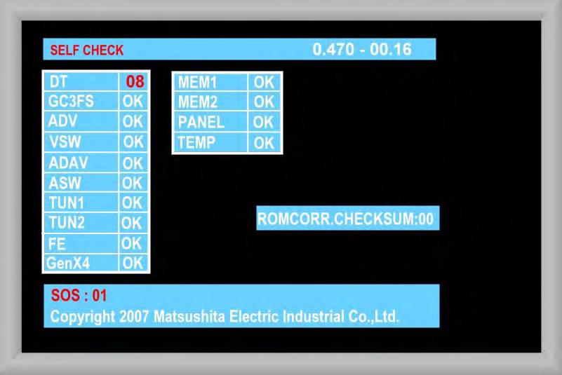
90 Self-Check Menu 90

91 Check point 91
92 Serviceman Mode To Toenter the the Serviceman Mode, turn turn the the TV TV on on and and while pressing the the VOLUME ((--) ) button on on the the main unit, unit, press the the RECALL button of of the the remote control three times within 3 seconds. To To exit the the Serviceman Mode, Press the the Power button on on the the TV TV or or the the Remote Control. 92
93 Serviceman Mode Menu and Navigation NOTE: This is not part of the Menu Key command 1 button...main items Selection in forward direction 2 button...main items Selection in reverse direction 3 button...sub items Selection in forward direction 4 button...sub items Selection in reverse direction VOL button...value of sub items change in forward direction ( + ), in reverse direction ( - ) 93

94 Adjustment Sub Menu 94
![Internal Test Patterns To access the internal patterns, select [AGING] from the main adjustment menu and press the [3] or [4] button of the remote](/docs-images/91/104494414/images/95-0.jpg "control to select the desired pattern. To To exit the the Serviceman Mode, Press the the Power button on on the the TV TV or or the the Remote Control.")
95 Internal Test Patterns To access the internal patterns, select [AGING] from the main adjustment menu and press the [3] or [4] button of the remote control to select the desired pattern. To To exit the the Serviceman Mode, Press the the Power button on on the the TV TV or or the the Remote Control. 95


96 Driver Setup Adjustment Driver Set-up Item / Preparation 1. Input a white signal to one of the unit s video input. 2. Set the picture controls as follows: Picture menu: Vivid Normal: Set Aspect: Full Caution 1. Perform the Vsus adjustment. 2. Confirm the voltage level of VSCN. This should be done after the adjustment of Vad which should be -105V When Vad = -105V, Vscn voltage is 35V ±4V. Note: See the panel label for voltages that are not listed in the service manual. 96

97 Initialization Pulse Adjustment 1. Input a 100% White signal to the unit. 2. Set the picture controls as follows: Picture menu : Vivid Normal : Set Aspect : Full 3. Connect an Oscilloscope to test point TPSC1. Using VR6602, adjust (T2) for 195+/- 10µ Sec

98 Quick adjustment after P.C.B. exchange 1. Caution Wait 1 minute for the electrolytic capacitors to discharge before removing any PCB from the unit. 2. Quick adjustment after P.C.B. or Panel exchange 98 98
Panasonic Services Company
 Panasonic Services Company 9 TH Gen. Plasma Display Television National Training 1 Models Comparison Comparison Table TV- MODEL Resolution SD Card Guide EPG CableCARD slot in the Tuner PC Input TH-65PX600U
LX600 LCD TV Technical Information
 LX600 LCD TV Technical Information TC-32LX600 Outline Features Overall Block Diagram A Board Main Layout Power On Sequence Protection Shutdown Troubleshooting Adjustments 1 Features Model TC-LX60 TC-LX600
Panasonic Services Company National Training
 Panasonic Services Company National Training TH-42PX20U/TH-50PX20U TH-42PA20U/TH-37PA20U Plasma Display Panel GP6D Chassis Update Information Warning This service information is designed for experienced
103FHD_USA 11OCT06. Technical Guide. 103 Plasma Display Monitor. National Training
 Panasonic Service and Technology 03 Professional Models Company Technical Guide 03 Plasma Display Monitor National Training Panasonic Service and Technology 03 Professional Models Company Prepared by Jean
USER MANUAL. VP-435 Component / UXGA HDMI Scaler MODEL: P/N: Rev 13
 KRAMER ELECTRONICS LTD. USER MANUAL MODEL: VP-435 Component / UXGA HDMI Scaler P/N: 2900-000262 Rev 13 Contents 1 Introduction 1 2 Getting Started 2 2.1 Achieving the Best Performance 2 2.2 Safety Instructions
2002 DP-2X Chassis Projection Television Information INSTRUCTOR Alvie Rodgers C.E.T. (Chamblee, GA.)
") Dec 00 (ver g) Training Materials Prepared by: ALVIE RODGERS C.E.T. 00 and 00 MODEL RELEASE DIGITAL HD READY PTV Chassis Model # Aspect DP-7 5SWX0B 6X9 57SWX0B 65SWX0B DP-7D DP-6 DP- DP-G 57TWX0B 6X9 65TWX0B
Dec 00 (ver g) Training Materials Prepared by: ALVIE RODGERS C.E.T. 00 and 00 MODEL RELEASE DIGITAL HD READY PTV Chassis Model # Aspect DP-7 5SWX0B 6X9 57SWX0B 65SWX0B DP-7D DP-6 DP- DP-G 57TWX0B 6X9 65TWX0B
SingMai Electronics SM06. Advanced Composite Video Interface: DVI/HD-SDI to acvi converter module. User Manual. Revision th December 2016
 SM06 Advanced Composite Video Interface: DVI/HD-SDI to acvi converter module User Manual Revision 0.3 30 th December 2016 Page 1 of 23 Revision History Date Revisions Version 17-07-2016 First Draft. 0.1
CM-392-Video to HDMI Scaler Box ID#481
 CM-392-Video to HDMI Scaler Box ID#481 Operation Manual Introduction CM-392-Video to HDMI Scaler Box is designed to convert Composite and S-Video to Digital HDMI in a variety of HDTV resolutions. It handles
SingMai Electronics SM06. Advanced Composite Video Interface: HD-SDI to acvi converter module. User Manual. Revision 0.
 SM06 Advanced Composite Video Interface: HD-SDI to acvi converter module User Manual Revision 0.4 1 st May 2017 Page 1 of 26 Revision History Date Revisions Version 17-07-2016 First Draft. 0.1 28-08-2016
Video Scaler Pro with RS-232
 Video Scaler Pro with RS-232 - ID# 783 Operation Manual Introduction Features The Video Scaler Pro with RS-232 is designed to convert Composite S-Video and YCbCr signals to a variety of computer and HDTV
Projection Television
 S Training Manual Projection Television Circuit Description and Troubleshooting Course: TVP-08 Course Description and Troubleshooting: RA-4 Chassis Prepared by: National Training Department Sony Service
V25 V25+ WS WS WS WS V27 WS-65517
 2005 Down to1 HIGH SPEED TROUBLESHOOTING V25-V27 CHASSIS V25 V25+ WS-48515 WS-55615 WS-55515 WS-65615 WS-65515 WS-73615 V25++ WS-55815 WS-65815 WS-55517 V27 WS-65517 WS-73517 MITSUBISHI DIGITAL ELECTRONICS
HD Digital Set-Top Box Quick Start Guide
 HD Digital Set-Top Box Quick Start Guide Eagle Communications HD Digital Set-Top Box Important Safety Instructions WARNING TO REDUCE THE RISK OF FIRE OR ELECTRIC SHOCK, DO NOT EXPOSE THIS PRODUCT TO RAIN
Model 5240 Digital to Analog Key Converter Data Pack
 Model 5240 Digital to Analog Key Converter Data Pack E NSEMBLE D E S I G N S Revision 2.1 SW v2.0 This data pack provides detailed installation, configuration and operation information for the 5240 Digital
Video to DVI 1080p Scaler Box - ID# 796
 Video to DVI 1080p Scaler Box - ID# 796 Operation Manual Introduction Video to DVI 1080p Scaler Box is an upgraded design to convert Standard Definition Composite Video (CV) and S-Video (SV) signals to
Evolution Digital HD Set-Top Box Important Safety Instructions
 Evolution Digital HD Set-Top Box Important Safety Instructions 1. Read these instructions. 2. Keep these instructions. 3. Heed all warnings. 4. Follow all instructions. 5. Do not use this apparatus near
V26 Chassis V26+ Chassis V26++ Chassis WD WD WD WD WD WD-62825
 Digital Light Processing Projection Television V26 Chassis 2004 V26 Chassis V26+ Chassis V26++ Chassis WD-52525 WD-52725 WD-52825 WD-62525 WD-62725 WD-62825 Copyright 2004 Mitsubishi Digital Electronics,
MULTIDYNE INNOVATIONS IN TELEVISION TESTING & DISTRIBUTION DIGITAL VIDEO, AUDIO & DATA FIBER OPTIC MULTIPLEXER TRANSPORT SYSTEM
 MULTIDYNE INNOVATIONS IN TELEVISION TESTING & DISTRIBUTION INSTRUCTION MANUAL DVM-1000 DIGITAL VIDEO, AUDIO & DATA FIBER OPTIC MULTIPLEXER TRANSPORT SYSTEM MULTIDYNE Electronics, Inc. Innovations in Television
10 th Generation Plasma Panel Replacement
 10 th Generation Plasma Panel Replacement This seminar covers 10 th generation models Panasonic Service and Technology Company National Training Prepared by Cesar Perdomo Panasonic Service and Technology
Video to PC/HD Scaler Box. Operation Manual
 Video to PC/HD Scaler Box Operation Manual (1). Introduction Congratulations on your purchase of the Cypress Video Scaler CM-390. Our professional Video Scaler products have been serving the industry for
AES-402 Automatic Digital Audio Switcher/DA/Digital to Analog Converter
 Broadcast Devices, Inc. AES-402 Automatic Digital Audio Switcher/DA/Digital to Analog Converter Technical Reference Manual Broadcast Devices, Inc. Tel. (914) 737-5032 Fax. (914) 736-6916 World Wide Web:
Kramer Electronics, Ltd. USER MANUAL. Models: VP-715, Video To SXGA / HD Scaler VP-716, Video To SXGA / DVI / HD Scaler
 Kramer Electronics, Ltd. USER MANUAL Models: VP-715, Video To SXGA / HD Scaler VP-716, Video To SXGA / DVI / HD Scaler Contents Contents 1 Introduction 1 2 Getting Started 1 3 Overview 1 3.1 VP-715/6 Scaler
AES-404 Digital Audio Switcher/DA/Digital to Analog Converter
 Broadcast Devices, Inc. AES-404 Digital Audio Switcher/DA/Digital to Analog Converter Technical Reference Manual Broadcast Devices, Inc. Tel. (914) 737-5032 Fax. (914) 736-6916 World Wide Web: www.broadcast-devices.com
QIP7232 P2. Hybrid QAM/IP High-definition Set-top. Quick Start Guide
 QIP7232 P2 Hybrid QAM/IP High-definition Set-top Quick Start Guide Before You Begin Introduction Congratulations on receiving a Motorola QIP7232 Hybrid QAM/IP High-definition Set-top. This document will
Video to HDMI Scaler Box
 Video to HDMI Scaler Box Operation Manual CM-392 (1). Introduction Congratulations on your purchase of the Cypress Video Scaler CM-392. Our professional Video Scaler products have been serving the industry
Models 5360 and 5365 Four Channel Analog to Digital Video Converters and Embedders Data Pack
 Models 5360 and 5365 Four Channel Analog to Digital Video Converters and Embedders Data Pack E NSEMBLE D E S I G N S Revision 1.3 SW v2.2.1 This data pack provides detailed installation, configuration
CAUTION RISK OF ELECTRIC SHOCK NO NOT OPEN
 Evolution Digital HD Set-Top Box Important Safety Instructions 1. Read these instructions. 2. Keep these instructions. 3. Heed all warnings. 4. Follow all instructions. 5. Do not use this apparatus near
PRO-ScalerHD2V HDMI to VGA & Audio Scaler Converter. User s Guide. Made in Taiwan
 PRO-ScalerHD2V HDMI to VGA & Audio Scaler Converter User s Guide Made in Taiwan Congratulations for owning a gofanco product. Our products aim to meet all your connectivity needs wherever you go. Have
USER MANUAL. VP-419xl Video to SXGA/HD Scaler MODEL: P/N: Rev 7
 KRAMER ELECTRONICS LTD. USER MANUAL MODEL: VP-419xl Video to SXGA/HD Scaler P/N: 2900-000201 Rev 7 Contents 1 Introduction 1 2 Getting Started 2 2.1 Achieving the Best Performance 2 2.2 Safety Instructions
Stand-by condition 16.9 (430 mm) 3.4 (86 mm) 14.8 (377 mm) CLOSED CAPTION
 3.4 (86 mm) 14.8 (377 mm) CLOSED CAPTION") ORDER NO. ITD0411063C1 B19Canada:B07 Digital Media Receiver TU-PT700U GP7P Chassis Specifications Power Source 120 V AC, 60 Hz Power Consumption Maximum 45 W Stand-by condition 22 W Dimensions (W H D)
ORDER NO. ITD0411063C1 B19Canada:B07 Digital Media Receiver TU-PT700U GP7P Chassis Specifications Power Source 120 V AC, 60 Hz Power Consumption Maximum 45 W Stand-by condition 22 W Dimensions (W H D)
TFT LCD MONITOR USER MANUAL. L80AP and L101AP
 TFT LCD MONITOR USER MANUAL L80AP - 8.0 and L101AP - 10.1 Table Of Contents Table of contents/ Warning.... 2 Precautions...3 About this user manual and products / Items included in the delivery..... 4
Kramer Electronics, Ltd. USER MANUAL. Model: VP-419xl. Video To SXGA/HD Scaler
 Kramer Electronics, Ltd. USER MANUAL Model: VP-419xl Video To SXGA/HD Scaler Contents Contents 1 Introduction 1 2 Getting Started 1 2.1 Quick Start 1 3 Overview 3 4 Your VP-419xl Video to SXGA/HD Scaler
USER MANUAL. 27 Full HD Widescreen LED Monitor L27ADS
 USER MANUAL 27 Full HD Widescreen LED Monitor L27ADS TABLE OF CONTENTS 1 Getting Started 2 Control Panel/ Back Panel 3 On Screen Display 4 Technical Specs 5 Care & Maintenance 6 Troubleshooting 7 Safety
CP-255ID Multi-Format to DVI Scaler
 CP-255ID Multi-Format to DVI Scaler Operation Manual DISCLAIMERS The information in this manual has been carefully checked and is believed to be accurate. Cypress Technology assumes no responsibility
Display-Shoot M642HD Plasma 42HD. Re:source. DVS-5 Module. Dominating Entertainment. Revox of Switzerland. E 2.00
 of Display-Shoot M642HD Plasma 42HD DVS-5 Module Dominating Entertainment. Revox of Switzerland. E 2.00 Contents DVS Module Installation DSV Connection Panel HDMI output YCrCb analogue output DSV General
User Manual rev: Made in Taiwan
 CV-500S HDMI to Component/CVBS & Audio Scaler Converter User Manual rev: 131218 Made in Taiwan The CV-500S HDMI to Component/CVBS & Audio Scaler Converter has been tested for conformance to safety regulations
17 19 PROFESSIONAL LCD COLOUR MONITOR ART
 17 19 PROFESSIONAL LCD COLOUR MONITOR ART. 41657-41659 Via Don Arrigoni, 5 24020 Rovetta S. Lorenzo (Bergamo) http://www.comelit.eu e-mail:export.department@comelit.it WARNING: TO REDUCE THE RISK OF FIRE
KRAMER ELECTRONICS LTD. USER MANUAL MODEL: VP-434 Component/UXGA HDMI Scaler. P/N: Rev 6
 KRAMER ELECTRONICS LTD. USER MANUAL MODEL: VP-434 Component/UXGA HDMI Scaler P/N: 2900-000346 Rev 6 Contents 1 Introduction 1 2 Getting Started 2 2.1 Achieving the Best Performance 2 2.2 Safety Instructions
User's Manual. Rev 1.0
 User's Manual Rev 1.0 Digital TV sales have increased dramatically over the past few years while the sales of analog sets are declining precipitously. First quarter of 2005 has brought the greatest volume
BLOCK DIAGRAM. Brightness Control -120V. Vertical Blanking, FBT 30V 15V. Protection TDA8172 ( IC601) Circuit -12V 12V. H/V Sync Processor
 Circuit -12V 12V. H/V Sync Processor") BLOCK DIAGRAM H.V DY CDT H- Conver gence Dynamic Focus Static Focus Auto Beam Limit Heater ( ) Screen G1 < OSD > H / V POSITION H / V SIZE SPCC TRAPIZODE PIN BALANCE PARALLELOGRAM CORNERTRAP DDC ON/OFF
BLOCK DIAGRAM H.V DY CDT H- Conver gence Dynamic Focus Static Focus Auto Beam Limit Heater ( ) Screen G1 < OSD > H / V POSITION H / V SIZE SPCC TRAPIZODE PIN BALANCE PARALLELOGRAM CORNERTRAP DDC ON/OFF
Model 7130 HD Downconverter and Distribution Amplifier Data Pack
 Model 7130 HD Downconverter and Distribution Amplifier Data Pack E NSEMBLE D E S I G N S Revision 1.0 SW v1.0 www.ensembledesigns.com 7130-1 Contents MODULE OVERVIEW 3 Audio Handling 3 Control 3 Metadata
USER MANUAL. 22" Class Slim HD Widescreen Monitor L215DS
 USER MANUAL 22" Class Slim HD Widescreen Monitor L215DS TABLE OF CONTENTS 1 Getting Started Package Includes Installation 2 Control Panel / Back Panel Control Panel Back Panel 3 On Screen Display 4 Technical
USER MANUAL Full HD Widescreen LED Monitor L215ADS
 USER MANUAL 21.5 Full HD Widescreen LED Monitor L215ADS TABLE OF CONTENTS 1 Getting Started 2 Control Panel/ Back Panel 3 On Screen Display 4 Technical Specs 5 Care & Maintenance 6 Troubleshooting 7 Safety
Model 4455 ASI Serial Digital Protection Switch Data Pack
 Model 4455 ASI Serial Digital Protection Switch Data Pack Revision 1.5 SW v2.2.11 This data pack provides detailed installation, configuration and operation information for the 4455 ASI Serial Digital
FS1-X. Quick Start Guide. Overview. Frame Rate Conversion Option. Two Video Processors. Two Operating Modes
 FS1-X Quick Start Guide Overview Matching up and synchronizing disparate video and audio formats is a critical part of any broadcast, mobile or post-production environment. Within its compact 1RU chassis,
USER MANUAL Full HD Widescreen LED Monitor L215IPS
 USER MANUAL 21.5 Full HD Widescreen LED Monitor L215IPS TABLE OF CONTENTS 1 Getting Started 2 Control Panel/ Back Panel 3 On Screen Display 4 Technical Specs 5 Care & Maintenance 6 Troubleshooting 7 Safety
USER MANUAL. Kramer Electronics, Ltd. Models: VP-413, Video to WXGA Scaler. VP-414, Video to WXGA / HD Scaler. VP-415, Video to WXGA / DVI Scaler
 Kramer Electronics, Ltd. USER MANUAL! Models: VP-413, Video to WXGA Scaler VP-414, Video to WXGA / HD Scaler VP-415, Video to WXGA / DVI Scaler VP-416, Video to DVI-I / HD Scaler Contents Contents 1 Introduction
Brief Description of Circuit Functions. The brief ckt. description of V20 107E5 17 Monitor
 Exhibit 4 Brief Description of Circuit Functions The brief ckt. description of V20 107E5 17 Monitor 0. Functional Block Diagram 1. General Description 2. Description of Circuit Diagram A. Power Supply
Kramer Electronics, Ltd. USER MANUAL. Model: FC Analog Video to SDI Converter
 Kramer Electronics, Ltd. USER MANUAL Model: FC-7501 Analog Video to SDI Converter Contents Contents 1 Introduction 1 2 Getting Started 1 3 Overview 2 4 Your Analog Video to SDI Converter 3 5 Using Your
Re:connect M 203. RS232 Interface Revox. Dominating Entertainment. Revox of Switzerland. E 2.03
 of Re:connect M 203 RS232 Interface Revox Dominating Entertainment. Revox of Switzerland. E 2.03 Attention! After updating the firmware to version 2.00 or higher, we recommend completely resetting the
Quick Start Guide. Digital Research Technologies Inc. 4 Marconi, Irvine, CA For: DLCD26, DLCD32, DLCD42 & DLCD42P LCD Televisions
 Quick Start Guide Digital Research Technologies Inc. 4 Marconi, Irvine, CA 92618 For: DLCD26, DLCD32, DLCD42 & DLCD42P LCD Televisions 1 Distance recommendations: Always position the LCD TV set where sufficient
ACUBRITE 23 SS. Manual. Stainless Steel Chassis 23" LCD Display. Content
 ACUBRITE 23 SS Stainless Steel Chassis 23" LCD Display Manual Introduction... 2 Hardware Installation... 2 The Display Timing... 5 The Display Outline Dimensions... 6 The Display Controls... 7 The Screen
Technical Reference. ATSC TV A/D Controller FOR TFT LCD. Model : SKY-4100M. Copyright 2008 All Rights Reserved. REV.1.0_
 Technical Reference ATSC TV A/D Controller FOR TFT LCD Model : SKY-4100M Copyright 2008 All Rights Reserved REV.1.0_2008.06.05 Page 1/13 1. Description The SKY-4100 is an interface board for LCD/PDP panel
PRO-ScalerV2HD VGA to HDMI & Audio Scaler Converter. User s Guide. Made in Taiwan
 VGA to HDMI & Audio Scaler Converter User s Guide Made in Taiwan Congratulations for owning a gofanco product. Our products aim to meet all your connectivity needs wherever you go. Have fun with our products!
P-2 Installing the monitor (continued) Carry out as necessary
 Carry out as necessary") P-2 Installing the monitor (continued) Carry out as necessary Using the monitor without the bezel MDT552S satisfies the UL requirements as long as it is used with the bezel attached. When using the monitor
P-2 Installing the monitor (continued) Carry out as necessary Using the monitor without the bezel MDT552S satisfies the UL requirements as long as it is used with the bezel attached. When using the monitor
HL32D2A. HL32D2A Page 1 of 13
 This document provide two levels of support; customer advice provides information that meant to be shared with the customer explaining possible operation issues that may be creating problems. Service assistance
User Instruction Manual IQSDA30/IQSDA32. Intelligent Reclocking High Performance HD-SDI/SD-SDI Distribution Amplifiers. snellgroup.
 User Instruction Manual IQSDA30/IQSDA32 Intelligent Reclocking High Performance HD-SDI/SD-SDI Distribution Amplifiers snellgroup.com IQSDA30/IQSDA32 www.snellgroup.com Information and Notices Information
Brief Description of Circuit Functions
 Exhibit 4 Brief Description of Circuit Functions Function Description for Hudson4 190P5 1. General 190P5 is the newest generation of Hudson 19 TFT Flat Panel Display Monitor. It designed with hyper integrity,
Scart/Video to HDMI Scaler Box
 Scart/Video to HDMI Scaler Box Operation Manual CM-393 (1). Introduction: Congratulations on your purchase of the Video Scaler CM-393. Our professional Video Scaler products have been serving the industry
USER MANUAL Full HD Widescreen LED Monitor L236VA
 USER MANUAL 23.6 Full HD Widescreen LED Monitor L236VA TABLE OF CONTENTS 1 Getting Started 2 Control Panel/ Back Panel 3 On Screen Display 4 Technical Specs 5 Care & Maintenance 6 Troubleshooting 7 Safety
TeamWork Kits Installation Guide
 TX 0 RX COM +5V APARATUS US TeamWork Kits Installation Guide TeamWork 400 and TeamWork 600 Kits The TeamWork 400 and TeamWork 600 kits consist of an HDMI switcher, system controller, Cable Cubby, and cables
USER MANUAL. 27 Full HD Widescreen LED Monitor L270E
 USER MANUAL 27 Full HD Widescreen LED Monitor L270E TABLE OF CONTENTS 1 Getting Started 2 Control Panel/ Back Panel 3 On Screen Display 4 Technical Specs 5 Care & Maintenance 6 Troubleshooting 7 Safety
Dell Wyse 5030 PCoIP Zero Client
 Dell Wyse 5030 PCoIP Zero Client User Guide Regulatory Model: PxN Regulatory Type: PxN001 Notes, cautions, and warnings NOTE: A NOTE indicates important information that helps you make better use of your
PN42A450P1D/ PN50A450P1D
 PN4A450PD/ PN50A450PD -800-SAMSUNG (767864) Samsung Electronics America, Inc. 05 Challenger Road Ridgefield Park, NJ 07660-05 Samsung Electronics Canada Inc., Customer Service 55 Standish Court Mississauga,
Displays Open Frame Monitor Model Number: AND-TFT-150Bxx
 Displays 15.0 Open Frame Monitor Model Number: AND-TFT-150Bxx The AND-TFT-150Bxx 15.0 Open Frame Monitor series are rugged, high performance Industrial LCD Monitors, designed for commercial and industrial
16 Stage Bi-Directional LED Sequencer
 16 Stage Bi-Directional LED Sequencer The bi-directional sequencer uses a 4 bit binary up/down counter (CD4516) and two "1 of 8 line decoders" (74HC138 or 74HCT138) to generate the popular "Night Rider"
Presented by: Amany Mohamed Yara Naguib May Mohamed Sara Mahmoud Maha Ali. Supervised by: Dr.Mohamed Abd El Ghany
 Presented by: Amany Mohamed Yara Naguib May Mohamed Sara Mahmoud Maha Ali Supervised by: Dr.Mohamed Abd El Ghany Analogue Terrestrial TV. No satellite Transmission Digital Satellite TV. Uses satellite
FS3. Quick Start Guide. Overview. FS3 Control
 FS3 Quick Start Guide Overview The new FS3 combines AJA's industry-proven frame synchronization with high-quality 4K up-conversion technology to seamlessly integrate SD and HD signals into 4K workflows.
Instruction Guide. Component/Composite/S-Video to DVI-D/HDTV Scaler and Converter Component/Composite/S-Video to VGA/HDTV Scaler and Converter
 VIDEO SCALER Component/Composite/S-Video to DVI-D/HDTV Scaler and Converter Component/Composite/S-Video to VGA/HDTV Scaler and Converter VID2DVIDTV (DVI) VID2VGATV (VGA) Instruction Guide * Actual product
39" 1080p LCD Television PLCD3992A
 PROSCAN 39" 1080p LCD Television PLCD3992A Contents Contents Caution Safety Information Unit and Accessories Product Feature 2 3 4 4 Introduction 5-9 1. Front View 5 2. Rear View 6 3. Instruction for
L, LTC, LTM, LT are registered trademarks of Linear Technology Corporation. Other product
 DESCRIPTION WARNING! Do not look directly at operating LED. This circuit produces light that can damage eyes. Demo Circuit 1265 QUICK START GUIDE LTC3220/LTC3220-1 360mA Universal 18-Channel LED Driver
CSLUX-300 Multi-Format to HDMI Scaler
 CSLUX-300 Multi-Format to HDMI Scaler Operation Manual DISCLAIMERS The information in this manual has been carefully checked and is believed to be accurate. Cypress Technology assumes no responsibility
Lite USER GUIDE. 3 Lite. For more information visit
 USER GUIDE Lite 3 Lite For more information visit www.caldigit.com Table of Contents Section 1 : General Information Introduction 3 General Use Warnings 3 Safety Warnings 3 System Requirements 4 In the
C8000. switch over & ducking
 features Automatic or manual Switch Over or Fail Over in case of input level loss. Ducking of a main stereo or surround sound signal by a line level microphone or by a pre recorded announcement / ad input.
Marshall Electronics. Pro A/V Communications VMV-402-SH. 3G/HD/SD-SDI Quad-viewer/Switcher with Audio Meter Display. User Manual.
 Marshall Electronics Pro A/V Communications VMV-402-SH 3G/HD/SD-SDI Quad-viewer/Switcher with Audio Meter Display User Manual Table of Contents 1. Introduction... 3 2. Features... 3 3. Package Contents...
Service Manual for D9100 Series Digital-Control Color Monitor
 Service Manual for D9100 Series Digital-Control Color Monitor Wells-Gardner Electronics 9500 W. 55 th Street Suite A McCook, Illinois 60525-3605 (708) 290-2100 069X3015-100 Revision: B / E01025 Date: 8-24-00
LedSync820C LED Video Processor USER S MANUAL
 LedSync820C LED Video Processor USER S MANUAL TABLE OF CONTENTS I. Safety precautions ----------------------------------------------------------------- 3 II. Connections of hardware 1.Rear view ------------------------------------------------------------
AUTOMATIC VIDEO LOSS A/B SWITCH
 CG-X AUTOMATIC VIDEO LOSS A/B SWITCH INSTRUCTION BOOK IB647502 TABLE OF CONTENTS DESCRIPTION 2 MOUNTING INSTRUCTIONS 3 HOW TO CABLE THE CG-X 3 POWER SUPPLY INSTALLATION 3 OPERATION 3 CARE AND MAINTENANCE
ESI VLS-2000 Video Line Scaler
 ESI VLS-2000 Video Line Scaler Operating Manual Version 1.2 October 3, 2003 ESI VLS-2000 Video Line Scaler Operating Manual Page 1 TABLE OF CONTENTS 1. INTRODUCTION...4 2. INSTALLATION AND SETUP...5 2.1.Connections...5
USER MANUAL. VP-422 HDMI to PC Scaler MODEL: P/N: Rev 5
 KRAMER ELECTRONICS LTD. USER MANUAL MODEL: VP-422 HDMI to PC Scaler P/N: 2900-000580 Rev 5 Contents 1 Introduction 1 2 Getting Started 2 2.1 Achieving the Best Performance 2 2.2 Safety Instructions 3
HD Leeza. Quick Setup Guide
 Page 1 of 15 Model KD-HD1080P Key Digital Video Processor Quick Setup Guide Have a question or a technical issue with your set-up? Call the Key Digital Hotline at: 866-439-8988 or 203-798-7187 E-mail the
DIGITAL VIDEO RECORDING (DVR) SERVICES
 SERVICES") DIGITAL VIDEO RECORDING (DVR) SERVICES With a Digital Video Recorder (DVR) set-top box, you can easily record your favorite programs and then play them back anytime. The DVR and Picture-In-Picture (PIP)
DIGITAL VIDEO RECORDING (DVR) SERVICES With a Digital Video Recorder (DVR) set-top box, you can easily record your favorite programs and then play them back anytime. The DVR and Picture-In-Picture (PIP)
VITEK VTM-TLM191 VTM-TLM240
 VTM-TLM191 VTM-TLM240 19 & 24 Professional LED Monitors with HDMI, VGA, and Looping BNC VITEK FEATURES 19 & 24 Wide Screen LED Display Panel HDMI, VGA, and Looping BNC Composite Video Inputs & Stereo Audio
SAFETY WARNINGS AND GUIDELINES
 SAFETY WARNINGS AND GUIDELINES Please read this manual thoroughly, paying extra attention to these safety warnings and guidelines: Do not expose this monitor to water or moisture of any kind. Do not handle
TFT LCD USER MANUAL TFT-15 TFT-17 TFT-19
 TFT15, 17, 19 Manual_Layout 2 01/03/2013 15:35 Page 1 TFT LCD monitor USER MANUAL TFT-15 TFT-17 TFT-19 TFT15, 17, 19 Manual_Layout 2 01/03/2013 15:35 Page 2 2 TFT15, 17, 19 Manual_Layout 2 01/03/2013 15:36
IQDDAC D to A Converter
 IQDDAC D to A Converter Module Description The IQDDAC module converts serial D1 format 270Mbits/sec data to analogue component video, in either YPbPr or GBR format. Functional Description The incoming
USER MANUAL. 28" 4K Ultra HD Monitor L28TN4K
 USER MANUAL 28" 4K Ultra HD Monitor L28TN4K TABLE OF CONTENTS 1 Getting Started 2 Control Panel/ Back Panel 3 On Screen Display 4 Technical Specs 5 Care & Maintenance 6 Troubleshooting 7 Safety Info &
USER MANUAL. 27" 2K QHD LED Monitor L27HAS2K
 USER MANUAL 27" 2K QHD LED Monitor L27HAS2K TABLE OF CONTENTS 1 Getting Started 2 Control Panel/ Back Panel 3 On Screen Display 4 Technical Specs 5 Troubleshooting 6 Safety Info & FCC warning 1 GETTING
Model 5250 Five Channel Digital to Analog Video Converter Data Pack
 Model 5250 Five Channel Digital to Analog Video Converter Data Pack E NSEMBLE D E S I G N S Revision 3.1 SW v2.0.1 This data pack provides detailed installation, configuration and operation information
ANALOG I/O MODULES AD268 / DA264 / TC218 USER S MANUAL
 UM-TS02 -E026 PROGRAMMABLE CONTROLLER PROSEC T2-series ANALOG I/O MODULES AD268 / DA264 / TC218 USER S MANUAL TOSHIBA CORPORATION Important Information Misuse of this equipment can result in property damage
Warranty Information
 Accuform Signs does not handle the warranty for the Digital Signage Displays. Please read below for details on the warranty of your product. If you are having trouble and need assistance, please contact
Exercise 1-2. Digital Trunk Interface EXERCISE OBJECTIVE
 Exercise 1-2 Digital Trunk Interface EXERCISE OBJECTIVE When you have completed this exercise, you will be able to explain the role of the digital trunk interface in a central office. You will be familiar
NTE1416 Integrated Circuit Chrominance and Luminance Processor for NTSC Color TV
 NTE1416 Integrated Circuit Chrominance and Luminance Processor for NTSC Color TV Description: The NTE1416 is an MSI integrated circuit in a 28 Lead DIP type package designed for NTSC systems to process
PATTERN GENERATOR PG-3D1X USER MANUAL V.2012PG-3D1X101.00
 PATTERN GENERATOR PG-3D1X USER MANUAL V.2012PG-3D1X101.00 Copyright and Trademarks: All rights reserved by C&C TECHNIC TAIWAN CO., LTD. No part of this document may be reproduced in any form or by any
PN50A550S1F/PN58A550S1F
 PN50A550SF/PN58A550SF -800-SAMSUNG (767864) Samsung Electronics America, Inc. 05 Challenger Road Ridgefield Park, NJ 07660-05 Samsung Electronics Canada Inc., Customer Service 55 Standish Court Mississauga,
4X1 Gefen TV Switcher GTV-HDMI N. User Manual
 4X1 Gefen TV Switcher GTV-HDMI1.3-441N User Manual INTRODUCTION Congratulations on your purchase of the 4x1 GefenTV Switcher. Your complete satisfaction is very important to us. GefenTV GefenTV is a unique
C Module Description
 IQMMX -Input Router & ASI Distribution Amplifier C Module Description The IQMMX is an ASI to 1 switch, distribution amplifier and transport stream switcher with up to 8 outputs in double width form or
C8188 C8000 1/10. digital audio modular processing system. 4 Channel AES/EBU I/O. features. block diagram. 4 balanced AES inputs
 features 4 balanced AES inputs Input Sample Rate Converters (SRC) 4 balanced AES outputs Relay bypass for pairs of I/Os Relay wait time after power up Master mode (clock master for the frame) 25pin Sub-D,
MULTIDYNE Electronics, Inc. Innovations in Television Testing & distribution
 INSTRUCTION MANUAL DVM-2200 DIGITAL VIDEO, AUDIO & DATA FIBER OPTIC MULTIPLEXER TRANSPORT SYSTEM MULTIDYNE Electronics, Inc. Innovations in Television Testing & distribution 1-(800)-4TV-TEST, 1-(800)-488-8378
Chapter 9 MSI Logic Circuits
 Chapter 9 MSI Logic Circuits Chapter 9 Objectives Selected areas covered in this chapter: Analyzing/using decoders & encoders in circuits. Advantages and disadvantages of LEDs and LCDs. Observation/analysis