Advanced Training Course on FPGA Design and VHDL for Hardware Simulation and Synthesis. 26 October - 20 November, 2009
|
|
|
- Logan Carr
- 5 years ago
- Views:
Transcription
1 Advanced Training Course on FPGA Design and VHDL for Hardware Simulation and Synthesis 26 October - 20 November, 2009 Starting to make an FPGA Project Alexander Kluge PH ESE FE Division CERN 385, rte Mayrin CH-1211 Geneva 23 Switzerland
2 Starting to make an FPGA project
3 FPGA specifications How to make an FPGA? What should it do? How should it do it? Systems / Requirements define detailed implementation scheme/architecture Specification need to be worked out before even one thinks about the FPGA type or code. Specification: understand user needs define specification of system together with user/costumer re-discuss, re-negotiate understand task of designer to understand and translate specifications
4 FPGA specifications Costumer/boss says: I need a system which can calculate the value each 25 ns. What you might understand is: The calculation needs to be finished within 25 ns What he means is: A new value needs to be processed every 25 ns. How long it takes to present the result does not matter First case: might be impossible, maybe not. Second case: Processors in parallel or in pipeline
5 Adder Example: add bit values in 25 ns data0 data_int (15 downto 0) data1 data2 data3 data4 data5 data6 data7 adder data15 sum(19 downto 0)

6 24 20
7
8
9 Adder 533 logic elements, 6% 278 pins, 74% 29.7 MHz => 33.6 ns 33.6 ns > 25 ns -> too slow
10 Adder 533 logic elements, 6% 278 pins, 74% 29.7 MHz => 33.6 ns 33.6 ns > 25 ns -> too slow Ask boss to buy faster, more expensive FPGA Work (manually) on FPGA placing&routing Help synthesizer to make fater adder Ask whether you have understood specification
11 FPGA specifications Costumer/boss says: I need a system which can calculate the value each 25 ns. What you might understand is: The calculation needs to be finished within 25 ns What he means is: A new value needs to be processed every 25 ns. How long it takes to present the result does not matter First case: might be impossible, maybe not. Second case: Processors in parallel or in pipeline
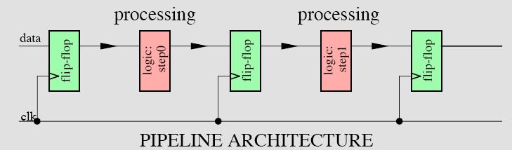
12 Pipeline architecture
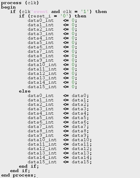
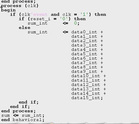
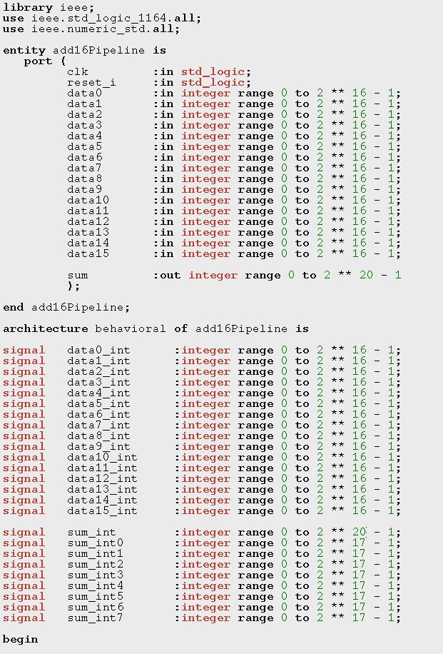
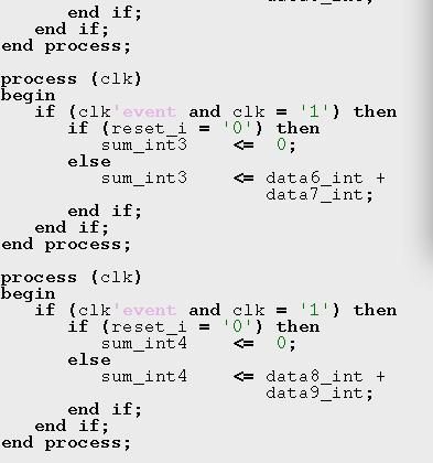
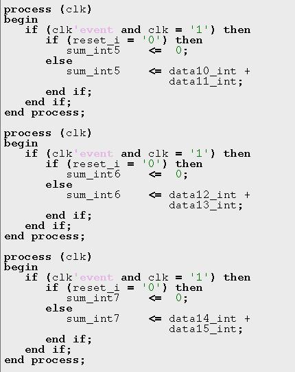
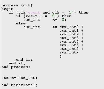
13 Adder with pipeline Example: add bit values every 25 ns data0 data1 data2 data3 data4 data5 data6 data7 data15 data_int (15 downto 0) adder adder adder adder adder reg reg reg reg reg adder sum(19 downto 0)
14
15

16 24 20
17
18
19
20 Adder with pipeline Adder without pipeline 533 logic elements, 6% 278 pins, 74% 29.7 MHz => 33.6 ns Adder with pipeline 526 logic elements, 6% 278 pins, 74% 45.4 MHz => 22 ns 22ns < 25 ns, fast enough and less logic
21 FPGA specifications re-discuss, re-negotiate understand task of designer to understand and translate specifications
22 Readout Processors
23 Read-out processors Specification Challenge - many parallel inputs 25 ns intervall - short processing time Storage during trigger decision time Data reduction/encoding (zero suppression) pipelining, buffering (FIFO, dual port RAM)
24 Pixel detector What do we need to know?
25 Silicon Sensor Position resolution: 10 µm light material: 1 % X 0 oder 2 mm Dez. 11, 2007 A. Kluge
26 Silicon Sensors V ext n-bulk p + Dez. 11, 2007 P. Riedler A. Kluge

27 Silicon Pixel sensors Dez. 11, 2007 P. Riedler A. Kluge

28 Silicon Pixel Wafers silicon sensor mm x mm 200 µm thin 160 x 256 pixel 425 µm x 50 µm Dez. 11, 2007 P. Riedler A. Kluge
29 Pixel read out chip Time resolution: 25 ns Repetition frequency: 40 MHz Storage time: > 3.2 µs Dez. 11, 2007 A. Kluge

30 Pixel chip Dez. 11, 2007 A. Kluge
31 Pixel detector 1 sensor 1 sensor 10 readout chips Image:INFN(Padova) Sept 3-7, 2007 A. Kluge


32 Pixel detector 1 sensor 1 sensor 10 readout chips Image:INFN(Padova) Sept 3-7, 2007 A. Kluge
33 Pixel detector
34 Pixel detector Full detector 120 x 2560 x MHz (100ns) = ~ 100 Gbits/s Separate read-out for each detector module Each detector module (10 chips) 1 x 2560 x MHz
35 Data funnel Data generator Data preprocessor Data processor Data merging
36 Data funnel Data Read-out generator ASIC Data Read-out preprocessor controller ASIC 1200 x 256 x MHz (100 ns) = ~100 Gbit/s 120 x 2560 x MHz (100 ns) = ~100 Gbit/s Data Link processor receiver FPGA Data Router merging FPGA 60 x 2 x 2560 x MHz (100 ns) = 60 x 1.6 Gbit/s 20 x 6 x 2560 x 32 bits * 10 MHz (100 ns) = 20 x 10 kbit/s
37 Pixel detector Data generator 2560 x 32 bits
38 Pixel detector What is the strategy? Some body counts values all the time, find out whether they can be divided by three, what to you do in real life? Include serial and dpm
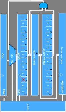
39 Pixel detector channel1-5 serializer de-serializer FIFO zero suppress & address decoder dual port memory channel multiplexer
40 Pixel detector serializer de-serializer FIFO zero suppress & address decoder dual port memory
41 Pixel detector data processing check if any hits if no hits -> load new value from FIFO if 1 hit only -> decode the hit & request new value from FIFO if more than one hit -> decode the hits
42 Pixel detector data processing How to decode the address? this line has two hits the state machine must send two hits into the dual port memory row address row address hit position = 5 hit position = 11
43 Pixel detector data processing Do we know enough to start the project? How do we encode the address? row address row address hit position = 5 hit position = 11
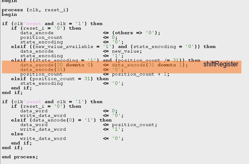
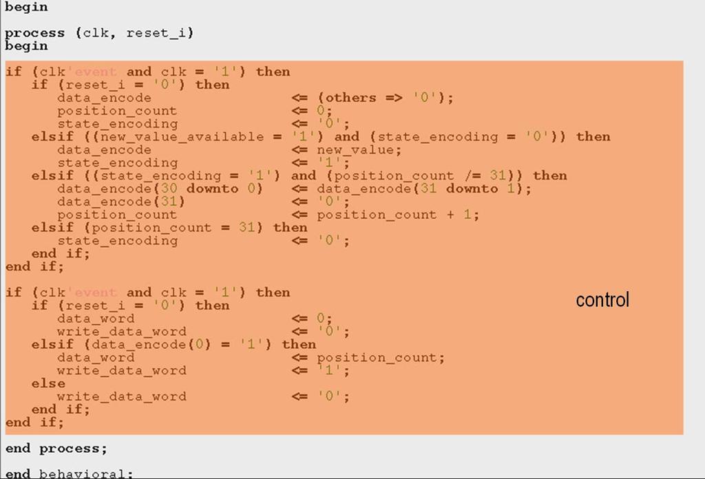
44 Pixel detector data processing read FIFO control parallelload shiftenable shiftregister serialout cntenable counter writeenable dual port memory

45 Position decoder shift register

46 Position decoder shift register

47 Position decoder shift register VHDL code
48
49
50
51


52 state machine with case statement
53 Shift register is a parallel load register
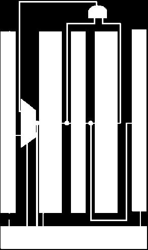
54 Position decoder shift register " "
55 Position decoder shift register

56 Position decoder shift register
57 Position decoder shift register Shift register & counter (if then) Result in an FPGA from 2002: (Altera EP20k200FC484-3) 81 out of 8320 logic elements 44 registers % (41/376) of pins 10.6 ns (94.5 MHz) position_count-> position_count tco: 8.0 ns: data_word_reg -> data_word tsu: 7.0 ns: new_value_available -> data_encode
58 Position decoder shift register Shift register & counter (case) Result in an FPGA from 2002: (Altera EP20k200FC484-3) 50 out of 8320 logic elements (with case statement) 44 registers % (41/376) of pins 9.1 ns (109.9 MHz) position_count-> data_encode tco: 7.0 ns: data_word_reg -> data_word tsu: 6.3 ns: new_value_available -> data_encode
59 Position decoder shift register Task fulfilled? Few logic cells Timing constraints fulfilled User requirements fulfilled? Processing per 32 bit line takes: 32 bits * 25 ns = 800 ns Data comes each 100 ns -> 1 out of bit line Decoding time for all lines is: 2560 * 800 ns => 2 ms Within 2 ms => data lines arrive input FIFO would need to be at least 20k * 32 bit deep During 2 ms no other trigger acquisition can take place dead time => max trigger rate: 488 Hz User requirements not fulfilled
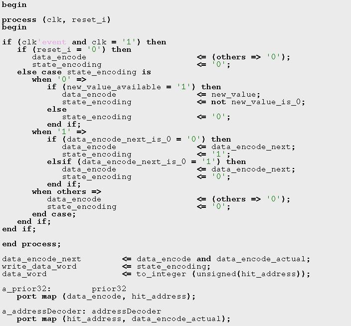
60 Position decoder priority encoder How to decode the address? this line has two hits the state machine must send two hits into the dual port memory row address hit position = 5 row address hit position = 11
61 Position decoder priority encoder read FIFO sel mux control register load priority encoder address decoder writeenable dual port memory
62 Position decoder priority encoder
63
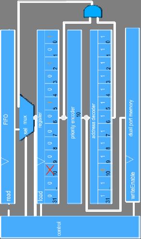
64
65
66
67

68 Position decoder priority encoder

69 Position decoder priority encoder
70 Position decoder priority encoder

71 Position decoder priority encoder
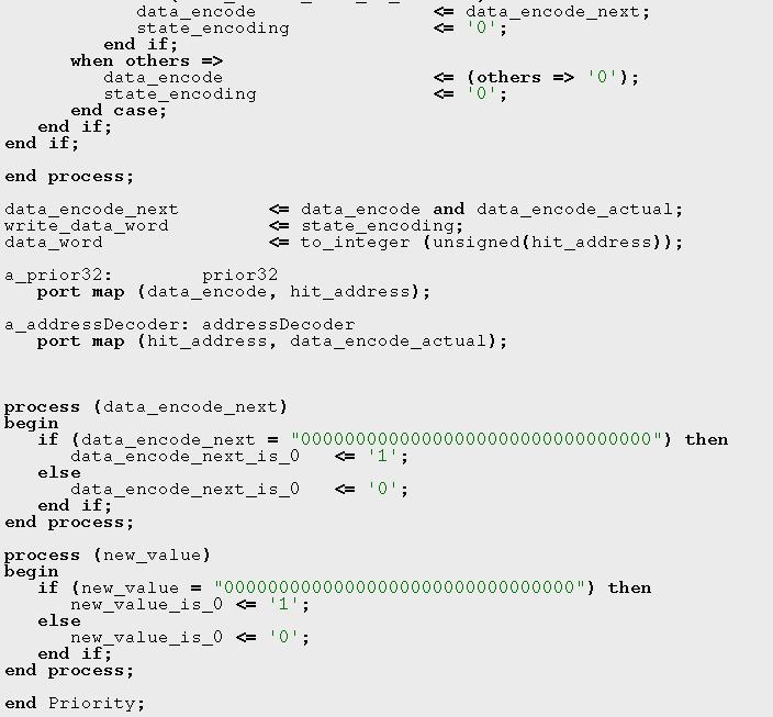
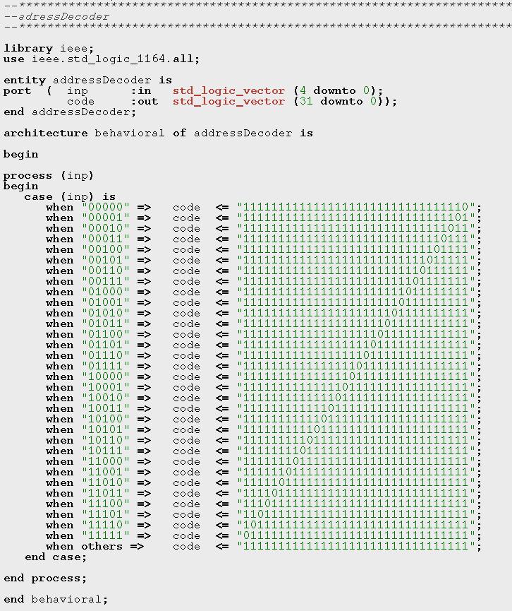
72 Position decoder priority encoder Priority encoder Result in an FPGA from 2002: (Altera EP20k200FC484-3) 172 (out of 8320) logic elements 33 registers addressdecoder: 16 prior32: 54 11% (41/376) of pins 20.8 ns (48.0 MHz) data_encode -> state_encoding tco: tsu: 17.1 ns:data_encode -> data_word 14.9 ns:new_value -> state_encoding
73 Position decoder priority encoder Priority encoder Result in an FPGA from 2002: (Altera EP20k200FC484-3) 172 (out of 8320) logic elements -> more logic cells 33 registers addressdecoder: 16 prior32: 54 11% (41/376) of pins 20.8 ns (48.0 MHz) data_encode -> state_encoding -> slower state machine, but faster processing tco: 17.1 ns:data_encode -> data_word tsu: 14.9 ns:new_value -> state_encoding
74 Position decoder priority encoder Task fulfilled? Many logic cells FPGA Timing constraints fulfilled User requirements fulfilled? Processing per 32 bit line takes: numbhits per line * 25 ns =? Data comes each 100 ns -> one out of bit line Decoding time for all lines is: 2560 *? ns =>? ms Within? ms =>? data lines arrive input FIFO would need to be at least? * 32 bit deep During? ms no other trigger acquisition can take place dead time => max trigger rate:? Hz User requirements fulfilled?
75 Position decoder priority encoder Task fulfilled? Physics simulation: max 2% of all pixels will be hit in one acquisition User requirements fulfilled? Processing per 32 bit line takes: (numbhits per line) * 25 ns = (32 * 0.02) * 25 ns = <25 ns Data comes each 100 ns -> one out of bit line One line with up to 4 hits can be decoded before the next line arrives Input FIFO of 1000 * 32 bits implemented to buffer statistical fluctuations or calibration sequences Dead time defined by transmission of data stream 2560 lines each 100 ns => 256 µs => 3900 Hz dead time => max trigger rate: 3900 Hz User requirements fulfilled: yes
76 Position decoder priority encoder Priority encoder Result in an FPGA from 2002: (Altera EP20k200FC484-3) 172 (out of 8320) logic elements -> more logic cells ns (48.0 MHz) data_encode -> state_encoding -> slower state machine, but faster processing Slower and more logic can mean more elegant and effective
77 Position decoder priority encoder User requirements fulfilled: yes Can we do better? Can we do faster or with less logic? Do we know something which the synthesizer does not know?
78
79

80 Position decoder priority encoder
81 Position decoder priority encoder Knowledge of implementation in target technology is important Knowledge of what the synthesizer is doing is important

82 Processor board with optical inputs 12 channels Parallel optical receiver module 12 closely packed G-link deserializer ASICs
The Read-Out system of the ALICE pixel detector
 The Read-Out system of the ALICE pixel detector Kluge, A. for the ALICE SPD collaboration CERN, CH-1211 Geneva 23, Switzerland Abstract The on-detector electronics of the ALICE silicon pixel detector (nearly
LHCb and its electronics. J. Christiansen On behalf of the LHCb collaboration
 LHCb and its electronics J. Christiansen On behalf of the LHCb collaboration Physics background CP violation necessary to explain matter dominance B hadron decays good candidate to study CP violation B
The ALICE on-detector pixel PILOT system - OPS
 The ALICE on-detector PILOT system - OPS Kluge, A. 1, Anelli, G. 1, Antinori, F. 2, Ban, J. 3, Burns, M. 1, Campbell, M. 1, Chochula, P. 1, 4, Dinapoli, R. 1, Formenti, F. 1,van Hunen, J.J. 1, Krivda,
Large Area, High Speed Photo-detectors Readout
 Large Area, High Speed Photo-detectors Readout Jean-Francois Genat + On behalf and with the help of Herve Grabas +, Samuel Meehan +, Eric Oberla +, Fukun Tang +, Gary Varner ++, and Henry Frisch + + University
Objectives. Combinational logics Sequential logics Finite state machine Arithmetic circuits Datapath
 Objectives Combinational logics Sequential logics Finite state machine Arithmetic circuits Datapath In the previous chapters we have studied how to develop a specification from a given application, and
University of Oxford Department of Physics. Interim Report
 University of Oxford Department of Physics Interim Report Project Name: Project Code: Group: Version: Atlas Binary Chip (ABC ) NP-ATL-ROD-ABCDEC1 ATLAS DRAFT Date: 04 February 1998 Distribution List: A.
Digilent Nexys-3 Cellular RAM Controller Reference Design Overview
 Digilent Nexys-3 Cellular RAM Controller Reference Design Overview General Overview This document describes a reference design of the Cellular RAM (or PSRAM Pseudo Static RAM) controller for the Digilent
Level and edge-sensitive behaviour
 Level and edge-sensitive behaviour Asynchronous set/reset is level-sensitive Include set/reset in sensitivity list Put level-sensitive behaviour first: process (clock, reset) is begin if reset = '0' then
DXP-xMAP General List-Mode Specification
 DXP-xMAP General List-Mode Specification The xmap processor can support a wide range of timing or mapping operations, including mapping with full MCA spectra, multiple SCA regions, and finally a variety
PIXEL2000, June 5-8, FRANCO MEDDI CERN-ALICE / University of Rome & INFN, Italy. For the ALICE Collaboration
 PIXEL2000, June 5-8, 2000 FRANCO MEDDI CERN-ALICE / University of Rome & INFN, Italy For the ALICE Collaboration CONTENTS: Introduction: Physics Requirements Design Considerations Present development status
CSCB58 - Lab 4. Prelab /3 Part I (in-lab) /1 Part II (in-lab) /1 Part III (in-lab) /2 TOTAL /8
 /1 Part II (in-lab) /1 Part III (in-lab) /2 TOTAL /8") CSCB58 - Lab 4 Clocks and Counters Learning Objectives The purpose of this lab is to learn how to create counters and to be able to control when operations occur when the actual clock rate is much faster.
CSCB58 - Lab 4 Clocks and Counters Learning Objectives The purpose of this lab is to learn how to create counters and to be able to control when operations occur when the actual clock rate is much faster.
Why FPGAs? FPGA Overview. Why FPGAs?
 Transistor-level Logic Circuits Positive Level-sensitive EECS150 - Digital Design Lecture 3 - Field Programmable Gate Arrays (FPGAs) January 28, 2003 John Wawrzynek Transistor Level clk clk clk Positive
A video signal processor for motioncompensated field-rate upconversion in consumer television
 A video signal processor for motioncompensated field-rate upconversion in consumer television B. De Loore, P. Lippens, P. Eeckhout, H. Huijgen, A. Löning, B. McSweeney, M. Verstraelen, B. Pham, G. de Haan,
Design, Realization and Test of a DAQ chain for ALICE ITS Experiment. S. Antinori, D. Falchieri, A. Gabrielli, E. Gandolfi
 Design, Realization and Test of a DAQ chain for ALICE ITS Experiment S. Antinori, D. Falchieri, A. Gabrielli, E. Gandolfi Physics Department, Bologna University, Viale Berti Pichat 6/2 40127 Bologna, Italy
COE328 Course Outline. Fall 2007
 COE28 Course Outline Fall 2007 1 Objectives This course covers the basics of digital logic circuits and design. Through the basic understanding of Boolean algebra and number systems it introduces the student
Status of the CSC Track-Finder
 Status of the CSC Track-Finder D. Acosta, S.M. Wang University of Florida A.Atamanchook, V.Golovstov, B.Razmyslovich PNPI CSC Muon Trigger Scheme Strip FE cards Strip LCT card CSC Track-Finder LCT Motherboard
Half-Adders. Ch.5 Summary. Chapter 5. Thomas L. Floyd
 Digital Fundamentals: A Systems Approach Functions of Combinational Logic Chapter 5 Half-Adders Basic rules of binary addition are performed by a half adder, which accepts two binary inputs (A and B) and
Conceps and trends for Front-end chips in Astroparticle physics
 Conceps and trends for Front-end chips in Astroparticle physics Eric Delagnes Fabrice Feinstein CEA/DAPNIA Saclay LPTA/IN2P3 Montpellier General interest performances Fast pulses : bandwidth > ~ 300 MHz
A new Scintillating Fibre Tracker for LHCb experiment
 A new Scintillating Fibre Tracker for LHCb experiment Alexander Malinin, NRC Kurchatov Institute on behalf of the LHCb-SciFi-Collaboration Instrumentation for Colliding Beam Physics BINP, Novosibirsk,
Laboratory Exercise 4
 Laboratory Exercise 4 Polling and Interrupts The purpose of this exercise is to learn how to send and receive data to/from I/O devices. There are two methods used to indicate whether or not data can be
MUHAMMAD NAEEM LATIF MCS 3 RD SEMESTER KHANEWAL
 1. A stage in a shift register consists of (a) a latch (b) a flip-flop (c) a byte of storage (d) from bits of storage 2. To serially shift a byte of data into a shift register, there must be (a) one click
EEM Digital Systems II
 ANADOLU UNIVERSITY DEPARTMENT OF ELECTRICAL AND ELECTRONICS ENGINEERING EEM 334 - Digital Systems II LAB 3 FPGA HARDWARE IMPLEMENTATION Purpose In the first experiment, four bit adder design was prepared
A Fast Constant Coefficient Multiplier for the XC6200
 A Fast Constant Coefficient Multiplier for the XC6200 Tom Kean, Bernie New and Bob Slous Xilinx Inc. Abstract. We discuss the design of a high performance constant coefficient multiplier on the Xilinx
Lossless Compression Algorithms for Direct- Write Lithography Systems
 Lossless Compression Algorithms for Direct- Write Lithography Systems Hsin-I Liu Video and Image Processing Lab Department of Electrical Engineering and Computer Science University of California at Berkeley
A pixel chip for tracking in ALICE and particle identification in LHCb
 A pixel chip for tracking in ALICE and particle identification in LHCb K.Wyllie 1), M.Burns 1), M.Campbell 1), E.Cantatore 1), V.Cencelli 2) R.Dinapoli 3), F.Formenti 1), T.Grassi 1), E.Heijne 1), P.Jarron
DEPFET Active Pixel Sensors for the ILC
 DEPFET Active Pixel Sensors for the ILC Laci Andricek for the DEPFET Collaboration (www.depfet.org) The DEPFET ILC VTX Project steering chips Switcher thinning technology Simulation sensor development
The Readout Architecture of the ATLAS Pixel System
 The Readout Architecture of the ATLAS Pixel System Roberto Beccherle / INFN - Genova E-mail: Roberto.Beccherle@ge.infn.it Copy of This Talk: http://www.ge.infn.it/atlas/electronics/home.html R. Beccherle
TSIU03: Lab 3 - VGA. Petter Källström, Mario Garrido. September 10, 2018
 Petter Källström, Mario Garrido September 10, 2018 Abstract In the initialization of the DE2-115 (after you restart it), an image is copied into the SRAM memory. What you have to do in this lab is to read
Compact Muon Solenoid Detector (CMS) & The Token Bit Manager (TBM) Alex Armstrong & Wyatt Behn Mentor: Dr. Andrew Ivanov
 & The Token Bit Manager (TBM) Alex Armstrong & Wyatt Behn Mentor: Dr. Andrew Ivanov") Compact Muon Solenoid Detector (CMS) & The Token Bit Manager (TBM) Alex Armstrong & Wyatt Behn Mentor: Dr. Andrew Ivanov Part 1: The TBM and CMS Understanding how the LHC and the CMS detector work as a
Compact Muon Solenoid Detector (CMS) & The Token Bit Manager (TBM) Alex Armstrong & Wyatt Behn Mentor: Dr. Andrew Ivanov Part 1: The TBM and CMS Understanding how the LHC and the CMS detector work as a
READOUT ELECTRONICS FOR TPC DETECTOR IN THE MPD/NICA PROJECT
 READOUT ELECTRONICS FOR TPC DETECTOR IN THE MPD/NICA PROJECT S.Movchan, A.Pilyar, S.Vereschagin a, S.Zaporozhets Veksler and Baldin Laboratory of High Energy Physics, Joint Institute for Nuclear Research,
Advanced System LSIs for Home 3D Systems
 ASP-DAC2011 Session 8D-1 Advanced System LSIs for Home 3D Systems January 28, 2011 Takao Suzuki Panasonic Corporation Strategic Semiconductor Development Center Agenda 1. Overview of 3D Systems - Principles
EITF35: Introduction to Structured VLSI Design
 EITF35: Introduction to Structured VLSI Design Part 4.2.1: Learn More Liang Liu liang.liu@eit.lth.se 1 Outline Crossing clock domain Reset, synchronous or asynchronous? 2 Why two DFFs? 3 Crossing clock
Advanced Devices. Registers Counters Multiplexers Decoders Adders. CSC258 Lecture Slides Steve Engels, 2006 Slide 1 of 20
 Advanced Devices Using a combination of gates and flip-flops, we can construct more sophisticated logical devices. These devices, while more complex, are still considered fundamental to basic logic design.
Layout Decompression Chip for Maskless Lithography
 Layout Decompression Chip for Maskless Lithography Borivoje Nikolić, Ben Wild, Vito Dai, Yashesh Shroff, Benjamin Warlick, Avideh Zakhor, William G. Oldham Department of Electrical Engineering and Computer
Electrical and Telecommunications Engineering Technology_TCET3122/TC520. NEW YORK CITY COLLEGE OF TECHNOLOGY The City University of New York
 NEW YORK CITY COLLEGE OF TECHNOLOGY The City University of New York DEPARTMENT: SUBJECT CODE AND TITLE: COURSE DESCRIPTION: REQUIRED: Electrical and Telecommunications Engineering Technology TCET 3122/TC
ECE 263 Digital Systems, Fall 2015
 ECE 263 Digital Systems, Fall 2015 REVIEW: FINALS MEMORY ROM, PROM, EPROM, EEPROM, FLASH RAM, DRAM, SRAM Design of a memory cell 1. Draw circuits and write 2 differences and 2 similarities between DRAM
FRANCO MEDDI CERN-ALICE / University of Rome & INFN, Italy. For the ALICE Collaboration
 PIXEL2000, June 5-8, 2000 FRANCO MEDDI CERN-ALICE / University of Rome & INFN, Italy For the ALICE Collaboration JUNE 5-8,2000 PIXEL2000 1 CONTENTS: Introduction: Physics Requirements Design Considerations
PICOSECOND TIMING USING FAST ANALOG SAMPLING
 PICOSECOND TIMING USING FAST ANALOG SAMPLING H. Frisch, J-F Genat, F. Tang, EFI Chicago, Tuesday 6 th Nov 2007 INTRODUCTION In the context of picosecond timing, analog detector pulse sampling in the 10
Electronics procurements
 Electronics procurements 24 October 2014 Geoff Hall Procurements from CERN There are a wide range of electronics items procured by CERN but we are familiar with only some of them Probably two main categories:
EE178 Spring 2018 Lecture Module 5. Eric Crabill
 EE178 Spring 2018 Lecture Module 5 Eric Crabill Goals Considerations for synchronizing signals Clocks Resets Considerations for asynchronous inputs Methods for crossing clock domains Clocks The academic
BABAR IFR TDC Board (ITB): system design
: system design") BABAR IFR TDC Board (ITB): system design Version 1.1 12 december 1997 G. Crosetti, S. Minutoli, E. Robutti I.N.F.N. Genova 1. Introduction TDC readout of the IFR will be used during BABAR data taking to
BABAR IFR TDC Board (ITB): system design Version 1.1 12 december 1997 G. Crosetti, S. Minutoli, E. Robutti I.N.F.N. Genova 1. Introduction TDC readout of the IFR will be used during BABAR data taking to
Laboratory 4. Figure 1: Serdes Transceiver
 Laboratory 4 The purpose of this laboratory exercise is to design a digital Serdes In the first part of the lab, you will design all the required subblocks for the digital Serdes and simulate them In part
VHDL Design and Implementation of FPGA Based Logic Analyzer: Work in Progress
 VHDL Design and Implementation of FPGA Based Logic Analyzer: Work in Progress Nor Zaidi Haron Ayer Keroh +606-5552086 zaidi@utem.edu.my Masrullizam Mat Ibrahim Ayer Keroh +606-5552081 masrullizam@utem.edu.my
A TARGET-based camera for CTA
 A TARGET-based camera for CTA TeV Array Readout with GSa/s sampling and Event Trigger (TARGET) chip: overview Custom-designed ASIC for CTA, developed in collaboration with Gary Varner (U Hawaii) Implementation:
Hardware Implementation of Viterbi Decoder for Wireless Applications
 Hardware Implementation of Viterbi Decoder for Wireless Applications Bhupendra Singh 1, Sanjeev Agarwal 2 and Tarun Varma 3 Deptt. of Electronics and Communication Engineering, 1 Amity School of Engineering
Atlas Pixel Replacement/Upgrade. Measurements on 3D sensors
 Atlas Pixel Replacement/Upgrade and Measurements on 3D sensors Forskerskole 2007 by E. Bolle erlend.bolle@fys.uio.no Outline Sensors for Atlas pixel b-layer replacement/upgrade UiO activities CERN 3D test
EEE130 Digital Electronics I Lecture #1_2. Dr. Shahrel A. Suandi
 EEE130 Digital Electronics I Lecture #1_2 Dr. Shahrel A. Suandi 1-4 Overview of Basic Logic Functions Digital systems are generally built from combinations of NOT, AND and OR logic elements The combinations
The Readout Architecture of the ATLAS Pixel System. 2 The ATLAS Pixel Detector System
 The Readout Architecture of the ATLAS Pixel System Roberto Beccherle, on behalf of the ATLAS Pixel Collaboration Istituto Nazionale di Fisica Nucleare, Sez. di Genova Via Dodecaneso 33, I-646 Genova, ITALY
ECSE-323 Digital System Design. Datapath/Controller Lecture #1
 1 ECSE-323 Digital System Design Datapath/Controller Lecture #1 2 Synchronous Digital Systems are often designed in a modular hierarchical fashion. The system consists of modular subsystems, each of which
8 DIGITAL SIGNAL PROCESSOR IN OPTICAL TOMOGRAPHY SYSTEM
 Recent Development in Instrumentation System 99 8 DIGITAL SIGNAL PROCESSOR IN OPTICAL TOMOGRAPHY SYSTEM Siti Zarina Mohd Muji Ruzairi Abdul Rahim Chiam Kok Thiam 8.1 INTRODUCTION Optical tomography involves
Chapter 9 MSI Logic Circuits
 Chapter 9 MSI Logic Circuits Chapter 9 Objectives Selected areas covered in this chapter: Analyzing/using decoders & encoders in circuits. Advantages and disadvantages of LEDs and LCDs. Observation/analysis
CHAPTER 6 ASYNCHRONOUS QUASI DELAY INSENSITIVE TEMPLATES (QDI) BASED VITERBI DECODER
 BASED VITERBI DECODER") 80 CHAPTER 6 ASYNCHRONOUS QUASI DELAY INSENSITIVE TEMPLATES (QDI) BASED VITERBI DECODER 6.1 INTRODUCTION Asynchronous designs are increasingly used to counter the disadvantages of synchronous designs.
80 CHAPTER 6 ASYNCHRONOUS QUASI DELAY INSENSITIVE TEMPLATES (QDI) BASED VITERBI DECODER 6.1 INTRODUCTION Asynchronous designs are increasingly used to counter the disadvantages of synchronous designs.
EN2911X: Reconfigurable Computing Topic 01: Programmable Logic. Prof. Sherief Reda School of Engineering, Brown University Fall 2014
 EN2911X: Reconfigurable Computing Topic 01: Programmable Logic Prof. Sherief Reda School of Engineering, Brown University Fall 2014 1 Contents 1. Architecture of modern FPGAs Programmable interconnect
Task 4_B. Decoder for DCF-77 Radio Clock Receiver
 Embedded Processor Lab (EIT-EMS-546-L-4) Task 4_B FB Elektrotechnik und Informationstechnik Prof. Dr.-Ing. Norbert Wehn Dozent: Uwe Wasenmüller Raum 12-213, wa@eit.uni-kl.de Task 4_B Decoder for DCF-77
EECS150 - Digital Design Lecture 12 - Video Interfacing. Recap and Outline
 EECS150 - Digital Design Lecture 12 - Video Interfacing Oct. 8, 2013 Prof. Ronald Fearing Electrical Engineering and Computer Sciences University of California, Berkeley (slides courtesy of Prof. John
Massachusetts Institute of Technology Department of Electrical Engineering and Computer Science Introductory Digital Systems Laboratory
 Problem Set Issued: March 2, 2007 Problem Set Due: March 14, 2007 Massachusetts Institute of Technology Department of Electrical Engineering and Computer Science 6.111 Introductory Digital Systems Laboratory
EE178 Lecture Module 4. Eric Crabill SJSU / Xilinx Fall 2005
 EE178 Lecture Module 4 Eric Crabill SJSU / Xilinx Fall 2005 Lecture #9 Agenda Considerations for synchronizing signals. Clocks. Resets. Considerations for asynchronous inputs. Methods for crossing clock
Registers and Counters
 Registers and Counters A register is a group of flip-flops which share a common clock An n-bit register consists of a group of n flip-flops capable of storing n bits of binary information May have combinational
Review : 2 Release Date : 2019 Last Amendment : 2013 Course Code : SKEE 2742 Procedure Number : PK-UTM-FKE-(0)-10
-10") School Course Name : : ELECTRICAL ENGINEERING 2 ND YEAR ELECTRONIC DESIGN LAB Review : 2 Release Date : 2019 Last Amendment : 2013 Course Code : SKEE 2742 Procedure Number : PK-UTM-FKE-(0)-10 School of
School Course Name : : ELECTRICAL ENGINEERING 2 ND YEAR ELECTRONIC DESIGN LAB Review : 2 Release Date : 2019 Last Amendment : 2013 Course Code : SKEE 2742 Procedure Number : PK-UTM-FKE-(0)-10 School of
FPGA Design with VHDL
 FPGA Design with VHDL Justus-Liebig-Universität Gießen, II. Physikalisches Institut Ming Liu Dr. Sören Lange Prof. Dr. Wolfgang Kühn ming.liu@physik.uni-giessen.de Lecture Digital design basics Basic logic
The Silicon Pixel Detector (SPD) for the ALICE Experiment
 for the ALICE Experiment") The Silicon Pixel Detector (SPD) for the ALICE Experiment V. Manzari/INFN Bari, Italy for the SPD Project in the ALICE Experiment INFN and Università Bari, Comenius University Bratislava, INFN and Università
The Silicon Pixel Detector (SPD) for the ALICE Experiment V. Manzari/INFN Bari, Italy for the SPD Project in the ALICE Experiment INFN and Università Bari, Comenius University Bratislava, INFN and Università
CMS Conference Report
 Available on CMS information server CMS CR 1997/017 CMS Conference Report 22 October 1997 Updated in 30 March 1998 Trigger synchronisation circuits in CMS J. Varela * 1, L. Berger 2, R. Nóbrega 3, A. Pierce
Lab 4: Hex Calculator
 CpE 487 Digital Design Lab Lab 4: Hex Calculator 1. Introduction In this lab, we will program the FPGA on the Nexys2 board to function as a simple hexadecimal calculator capable of adding and subtracting
Use of Low Power DET Address Pointer Circuit for FIFO Memory Design
 International Journal of Education and Science Research Review Use of Low Power DET Address Pointer Circuit for FIFO Memory Design Harpreet M.Tech Scholar PPIMT Hisar Supriya Bhutani Assistant Professor
Reconfigurable Architectures. Greg Stitt ECE Department University of Florida
 Reconfigurable Architectures Greg Stitt ECE Department University of Florida How can hardware be reconfigurable? Problem: Can t change fabricated chip ASICs are fixed Solution: Create components that can
KEK. Belle2Link. Belle2Link 1. S. Nishida. S. Nishida (KEK) Nov.. 26, Aerogel RICH Readout
 Nov.. 26, Aerogel RICH Readout") S. Nishida KEK Nov 26, 2010 1 Introduction (Front end electronics) ASIC (SA) Readout (Digital Part) HAPD (144ch) Preamp Shaper Comparator L1 buffer DAQ group Total ~ 500 HAPDs. ASIC: 36ch per chip (i.e.
S. Nishida KEK Nov 26, 2010 1 Introduction (Front end electronics) ASIC (SA) Readout (Digital Part) HAPD (144ch) Preamp Shaper Comparator L1 buffer DAQ group Total ~ 500 HAPDs. ASIC: 36ch per chip (i.e.
FPGA Based Data Read-Out System of the Belle 2 Pixel Detector
 FPGA Based Read-Out System of the Belle 2 Pixel Detector Dmytro Levit, Igor Konorov, Daniel Greenwald, Stephan Paul Technische Universität München arxiv:1406.3864v1 [physics.ins-det] 15 Jun 2014 Abstract
CDA 4253 FPGA System Design FPGA Architectures. Hao Zheng Dept of Comp Sci & Eng U of South Florida
 CDA 4253 FPGA System Design FPGA Architectures Hao Zheng Dept of Comp Sci & Eng U of South Florida FPGAs Generic Architecture Also include common fixed logic blocks for higher performance: On-chip mem.
In-process inspection: Inspector technology and concept
 Inspector In-process inspection: Inspector technology and concept Need to inspect a part during production or the final result? The Inspector system provides a quick and efficient method to interface a
A CONTROL MECHANISM TO THE ANYWHERE PIXEL ROUTER
 University of Kentucky UKnowledge University of Kentucky Master's Theses Graduate School 2007 A CONTROL MECHANISM TO THE ANYWHERE PIXEL ROUTER Subhasri Krishnan University of Kentucky, skris0@engr.uky.edu
FPGA Implementation of Convolutional Encoder And Hard Decision Viterbi Decoder
 FPGA Implementation of Convolutional Encoder And Hard Decision Viterbi Decoder JTulasi, TVenkata Lakshmi & MKamaraju Department of Electronics and Communication Engineering, Gudlavalleru Engineering College,
DE2-115/FGPA README. 1. Running the DE2-115 for basic operation. 2. The code/project files. Project Files
 DE2-115/FGPA README For questions email: jeff.nicholls.63@gmail.com (do not hesitate!) This document serves the purpose of providing additional information to anyone interested in operating the DE2-115
The Alice Silicon Pixel Detector (SPD) Peter Chochula for the Alice Pixel Collaboration
 Peter Chochula for the Alice Pixel Collaboration") The Alice Silicon Pixel Detector (SPD) Peter Chochula for the Alice Pixel Collaboration The Alice Pixel Detector R 1 =3.9 cm R 2 =7.6 cm Main Physics Goal Heavy Flavour Physics D 0 K π+ 15 days Pb-Pb data
The Alice Silicon Pixel Detector (SPD) Peter Chochula for the Alice Pixel Collaboration The Alice Pixel Detector R 1 =3.9 cm R 2 =7.6 cm Main Physics Goal Heavy Flavour Physics D 0 K π+ 15 days Pb-Pb data
THE WaveDAQ SYSTEM FOR THE MEG II UPGRADE
 Stefan Ritt, Paul Scherrer Institute, Switzerland Luca Galli, Fabio Morsani, Donato Nicolò, INFN Pisa, Italy THE WaveDAQ SYSTEM FOR THE MEG II UPGRADE DRS4 Chip 0.2-2 ns Inverter Domino ring chain IN Clock
V6118 EM MICROELECTRONIC - MARIN SA. 2, 4 and 8 Mutiplex LCD Driver
 EM MICROELECTRONIC - MARIN SA 2, 4 and 8 Mutiplex LCD Driver Description The is a universal low multiplex LCD driver. The version 2 drives two ways multiplex (two blackplanes) LCD, the version 4, four
Inside Digital Design Accompany Lab Manual
 1 Inside Digital Design, Accompany Lab Manual Inside Digital Design Accompany Lab Manual Simulation Prototyping Synthesis and Post Synthesis Name- Roll Number- Total/Obtained Marks- Instructor Signature-
The Pixel Trigger System for the ALICE experiment
 CERN, European Organization for Nuclear Research E-mail: gianluca.aglieri.rinella@cern.ch The ALICE Silicon Pixel Detector (SPD) data stream includes 1200 digital signals (Fast-OR) promptly asserted on
Implementation of Low Power and Area Efficient Carry Select Adder
 International Journal of Engineering Science Invention ISSN (Online): 2319 6734, ISSN (Print): 2319 6726 Volume 3 Issue 8 ǁ August 2014 ǁ PP.36-48 Implementation of Low Power and Area Efficient Carry Select
Laboratory Exercise 7
 Laboratory Exercise 7 Finite State Machines This is an exercise in using finite state machines. Part I We wish to implement a finite state machine (FSM) that recognizes two specific sequences of applied
T1 Deframer. LogiCORE Facts. Features. Applications. General Description. Core Specifics
 November 10, 2000 Xilinx Inc. 2100 Logic Drive San Jose, CA 95124 Phone: +1 408-559-7778 Fax: +1 408-559-7114 E-mail: support@xilinx.com URL: www.xilinx.com/ipcenter Features Supports T1-D4 and T1-ESF
Hardware Implementation of Block GC3 Lossless Compression Algorithm for Direct-Write Lithography Systems
 Hardware Implementation of Block GC3 Lossless Compression Algorithm for Direct-Write Lithography Systems Hsin-I Liu, Brian Richards, Avideh Zakhor, and Borivoje Nikolic Dept. of Electrical Engineering
SciFi A Large Scintillating Fibre Tracker for LHCb
 SciFi A Large Scintillating Fibre Tracker for LHCb Roman Greim on behalf of the LHCb-SciFi-Collaboration 14th Topical Seminar on Innovative Particle Radiation Detectors, Siena 5th October 2016 I. Physikalisches
IMPLEMENTATION OF USB TRANSCEIVER MACROCELL INTERFACE
 IMPLEMENTATION OF USB TRANSCEIVER MACROCELL INTERFACE A. Vamshidhar Reddy 1, A.Laxman 2,.Prakash 3 L, T.Satyanarayana 4 1 Assoc.Prof. ECE Department, RRS COLLEGE OF ENG. & TECH.,AP,India,avamshireddy@gmail.com
Evaluation of an Optical Data Transfer System for the LHCb RICH Detectors.
 Evaluation of an Optical Data Transfer System for the LHCb RICH Detectors. N.Smale, M.Adinolfi, J.Bibby, G.Damerell, C.Newby, L.Somerville, N.Harnew, S.Topp-Jorgensen; University of Oxford, UK V.Gibson,
Microprocessor Design
 Microprocessor Design Principles and Practices With VHDL Enoch O. Hwang Brooks / Cole 2004 To my wife and children Windy, Jonathan and Michelle Contents 1. Designing a Microprocessor... 2 1.1 Overview
1ms Column Parallel Vision System and It's Application of High Speed Target Tracking
 Proceedings of the 2(X)0 IEEE International Conference on Robotics & Automation San Francisco, CA April 2000 1ms Column Parallel Vision System and It's Application of High Speed Target Tracking Y. Nakabo,
Microbolometer based infrared cameras PYROVIEW with Fast Ethernet interface
 DIAS Infrared GmbH Publications No. 19 1 Microbolometer based infrared cameras PYROVIEW with Fast Ethernet interface Uwe Hoffmann 1, Stephan Böhmer 2, Helmut Budzier 1,2, Thomas Reichardt 1, Jens Vollheim
Front End Electronics
 CLAS12 Ring Imaging Cherenkov (RICH) Detector Mid-term Review Front End Electronics INFN - Ferrara Matteo Turisini 2015 October 13 th Overview Readout requirements Hardware design Electronics boards Integration
Experiment: FPGA Design with Verilog (Part 4)
") Department of Electrical & Electronic Engineering 2 nd Year Laboratory Experiment: FPGA Design with Verilog (Part 4) 1.0 Putting everything together PART 4 Real-time Audio Signal Processing In this part
Department of Electrical & Electronic Engineering 2 nd Year Laboratory Experiment: FPGA Design with Verilog (Part 4) 1.0 Putting everything together PART 4 Real-time Audio Signal Processing In this part
Block Diagram. 16/24/32 etc. pixin pixin_sof pixin_val. Supports 300 MHz+ operation on basic FPGA devices 2 Memory Read/Write Arbiter SYSTEM SIGNALS
 Key Design Features Block Diagram Synthesizable, technology independent IP Core for FPGA, ASIC or SoC Supplied as human readable VHDL (or Verilog) source code Output supports full flow control permitting
Massachusetts Institute of Technology Department of Electrical Engineering and Computer Science Introductory Digital Systems Laboratory
 Problem Set Issued: March 3, 2006 Problem Set Due: March 15, 2006 Massachusetts Institute of Technology Department of Electrical Engineering and Computer Science 6.111 Introductory Digital Systems Laboratory
FPGA Based Implementation of Convolutional Encoder- Viterbi Decoder Using Multiple Booting Technique
 FPGA Based Implementation of Convolutional Encoder- Viterbi Decoder Using Multiple Booting Technique Dr. Dhafir A. Alneema (1) Yahya Taher Qassim (2) Lecturer Assistant Lecturer Computer Engineering Dept.
FPGA TechNote: Asynchronous signals and Metastability
 FPGA TechNote: Asynchronous signals and Metastability This Doulos FPGA TechNote gives a brief overview of metastability as it applies to the design of FPGAs. The first section introduces metastability
PRELIMINARY INFORMATION. Professional Signal Generation and Monitoring Options for RIFEforLIFE Research Equipment
 Integrated Component Options Professional Signal Generation and Monitoring Options for RIFEforLIFE Research Equipment PRELIMINARY INFORMATION SquareGENpro is the latest and most versatile of the frequency
1. Convert the decimal number to binary, octal, and hexadecimal.
 1. Convert the decimal number 435.64 to binary, octal, and hexadecimal. 2. Part A. Convert the circuit below into NAND gates. Insert or remove inverters as necessary. Part B. What is the propagation delay
Hardware Modeling of Binary Coded Decimal Adder in Field Programmable Gate Array
 American Journal of Applied Sciences 10 (5): 466-477, 2013 ISSN: 1546-9239 2013 M.I. Ibrahimy et al., This open access article is distributed under a Creative Commons Attribution (CC-BY) 3.0 license doi:10.3844/ajassp.2013.466.477
Spartan-II Development System
 2002-May-4 Introduction Dünner Kirchweg 77 32257 Bünde Germany www.trenz-electronic.de The Spartan-II Development System is designed to provide a simple yet powerful platform for FPGA development, which
Muon Forward Tracker. MFT Collaboration
 Muon Forward Tracker MFT Collaboration QGP France 2013 Introduction Summary of what «physically» MFT looks like: - Silicon detector - Data flow - Mechanical aspects - Power supplies - Cooling - Insertion/Extraction
Lab 6: Video Game PONG
 CpE 487 Digital Design Lab Lab 6: Video Game PONG 1. Introduction In this lab, we will extend the FPGA code we developed in Labs 3 and 4 (Bouncing Ball) to build a simple version of the 1970 s arcade game
Local Trigger Electronics for the CMS Drift Tubes Muon Detector
 Amsterdam, 1 October 2003 Local Trigger Electronics for the CMS Drift Tubes Muon Detector Presented by R.Travaglini INFN-Bologna Italy CMS Drift Tubes Muon Detector CMS Barrel: 5 wheels Wheel : Azimuthal