R&D on SOI Counting Pixel Chips
|
|
|
- Kerrie Craig
- 5 years ago
- Views:
Transcription
 Beijing, CHINA E-mail: yplu@ihep.ac.")
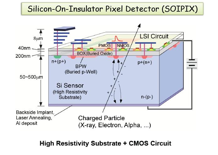
1 KEK Seminar 28 January 2015 Tsukuba R&D on SOI Counting Pixel Chips Yunpeng Lu Institute of High Energy Physics(IHEP) Beijing, CHINA
 700-meter deep")
2 JUNO Exp. 20K ton liquid scint. 3% energy resolution(at 1MeV) 700-meter deep underground 2
3 Outline Introduction to SOIPIX Motivation of Counting Pixel R&D Nested-Wells-based design CPIXTEG2 by A-R-Tec CPIXTEG3 DSOI-based design CPIXTEG3b Summary 3
4 4

5 5

6 SOIPIX Collaboration 6
7 Outline Introduction to SOIPIX Motivation of Counting Pixel R&D Nested-Wells-based design CPIXTEG2 by A-R-Tec CPIXTEG3 DSOI-based design CPIXTEG3b Summary 7

8 Motivation(1) Counting Pixel is an effective measure to study shielding effect in SOIPIX detectors. A key issue in SOI Pixel Technology Necessity of shielding recognized and understood by F. X. Pengg Counting pixel suffered from charge injection most, while integrating pixel not sensitive to it. 9.4kΩ/ 0.2kΩ/ not compatible with current process 8 more recent version: Nested-Wells more fancy thing: Double SOI Shielding-well proposed by F. X. Pengg in his dissertation Monolithic Silicon Pixel Detectors in SOI Technology Good in concept but not implemented successfully.
.")
9 Motivation(2) Counting Pixel is getting more and more popular in synchrotron radiation application due to superior performance. Macromolecular Crystallography, Small-Angle Scattering (SAXS) etc. Fast readout / no readout noise / High dynamic range /Sharp point spread function Targeted on the detector proposed by Prof. Shunji Kishimoto (PF, KEK). Very compact pixel circuit Very good S/N required Specifications: 30*30 um 2 pixel size 1k frames/s 14-bit counter Low energy X-ray 2~4 kev 9
10 Fundamental Issues Preamplifier Shaper On-chip circuit Amp-Sha-Disc system Counter and register in pixel Shielding (Charge Injection) Nested-wells Double SOI Leakage current Full depletion guaranteed Contribute to noise level but can be mitigated by low temperature Radiation damage Fine if back-illuminated by low energy X-ray -A -A DAC Discriminator Counter 10
11 Outline Introduction to SOIPIX Motivation of Counting Pixel R&D Nested-Wells-based design CPIXTEG2 by A-R-Tec CPIXTEG3 DSOI-based design CPIXTEG3b Summary 11
12 Amp-Sha-Disc in CPIXTEG2 A-R-Tec Preamplifer e - Cf ~4fF Shaper Vgain 2.5 Dual Discriminators Threshold window Hysteresis 12
13 Feedback and Leakage Compensation The krummenacher scheme used for preamplifier and shaper High gain amplifier in the core Leakage compensated by M 2 Feedback current set by I b = I 1 - I 2 Vout DC set by Vref Very popular in pixel circuit but it relys on the precise I 1 and I 2 Failure if I 2 > I 1 I 1 A-R-Tec -A I 2 The krummenacher scheme for P-in-N sensor 13
14 Discriminator A-R-Tec Hysteresis to avoid noise hit Vtn, threshold for a Low to High transition Vtp, threshold for a High to Low transition Vhyst > 3σ noise Global threshold set by Vth Local adjustment by a 4-bit DAC in pixel Principle of hysteresis Vin Vth Bit3 Bit2 Bit1 Bit0 4-bit DAC Schematics of discriminator and DAC 14

15 Discriminator A-R-Tec Hysteresis to avoid noise hit Vtn, threshold for a Low to High transition Vtp, threshold for a High to Low transition Vhyst > 3σ noise Global threshold set by Vth Local adjustment by a 4-bit DAC in pixel Principle of hysteresis Vin Vth Bit3 Bit2 Bit1 Bit0 4-bit DAC Schematics of discriminator and DAC 15


16 A-R-Tec Layout Chip size 5mm*5mm Pixel size 64um*64um 16-bit Counter & 10-bit Register Amp-Sha covered by Nested-wells Bias voltage limited due to back gate effect 64um 5mm COUNTER CPIXTEG2 Chip layout AMP&SHP REGISTER DISCRI. Nested-Wells CPIXTEG2 Pixel layout 16


17 Overview of CPIXTEG2 results A-R-Tec Amp-Sha-Disc system Counter and Register Bias and Aobuf Current Source variation Counter & Register access Shielding between analog and sense node Response of Light stimulus Shielding between counter and sense node not reported analog waveform 17


18 V b =20V V b =20V A-R-Tec Circuit behaviors with sensor connected Crosstalk between BPW and Transistors observed. Nested-wells is effective in shielding shaper. Shielding of discriminator and counter not evaluated yet. Failure of current mirror, overridden by external port. V b =1V VL_FB_AMP_N V b =20V 18
19 Outline Introduction to SOIPIX Motivation of Counting Pixel R&D Nested-Wells-based design CPIXTEG2 by A-R-Tec CPIXTEG3 DSOI-based design CPIXTEG3b Summary 19


20 Continuing efforts of Nested-wells on CPIXTEG3 Expand Nested-wells to full pixel To suppress back gate effect To evaluate shielding of digital part But large Cd due to BNW/BPW junction More BNW contacts BNW ~10KΩ/ A few bugs fixed BPW&BP2 BNW NS1 BNW contact CPIXTEG2 pixel layout CPIXTEG3 pixel layout PS Sense Node 20

21 Measurement of crosstalk from discriminator Repeated all results on CPIXTEG2 And found more: Discriminator crosstalk if overlapped with nested-wells PREAMP SHAPER Disable Disc. via VH2 Discriminator_High Discriminator_Low 1. Charge Injection with Discr. working Vtest = 600mV; VL_AMP_N = 280mV; Vdet = +5V 2. Charge injection with Discr. stopped 21


22 Measurement of crosstalk from counter Counter driven by external clock Watch the analog output Counter crosstalk large Clearly pattern related Largest on the transition between all 1 s and all 0 s Varing Vbnw and Vback, no change Not sufficient shielding PREAMP SHAPER DO_14 Counter_clk X011_1111_1111_1111 X100_0000_0000_0000 X111_1111_1111_1111 X000_0000_0000_ clks 16 clks X100_0000_0000_0111 X100_0000_0000_1000 X100_0000_0001_0111 X100_0000_0001_1000 X100_0000_0010_0111 X100_0000_0010_1000
23 Outline Introduction to SOIPIX Motivation of Counting Pixel R&D Nested-Wells-based design CPIXTEG2 by A-R-Tec CPIXTEG3 DSOI-based design CPIXTEG3b Summary 23
24 Design consideration for CPIXTEG3b A constant feedback current scheme adopted The krummenacher scheme would fail due to mismatch of current mirrors. Diode-biased-inverter discriminator Narrow threshold spreading reported Cut the pixel smaller 2->1 discriminator 16->6 bits counter 10->6 bits register 64um->50um pixel pitch New shielding scheme based on DSOI process Larger pixel array 64*64 24
25 Constant Current Feedback A constant current feedback used for Preamp and Shaper High gain amplifier in the core M1 in linear region and compensate leakage current when no hit M1 in saturation region and discharge C f by copying I b after a hit Avoid the risk of failure as in the krummenacher scheme Used in the ATLAS FEI pixel chips A constant current feedback scheme -A 25
26 Noise analysis by HSPICE simulation PREAMP Output n o = 1.4mV equivalent to 70 e - SHAPER Output n o = 6.8mV equivalent to 57 e - ENC (e - ) Shaper Output y = x Cd=100fF; Cf=5fF; Ccouple = 30fF Ifb_preamp = Ifb_shaper = 1nA; Leakage Current Noise not Included 1/f noise and channel thermal noise included Cd (ff) 26
27 Diode-biased-inverter discriminator AC coupled, baseline of shaper blocked Threshold voltages equals V diode /A I thr = I s (e Vdiode/VT -1) V T = kt/e Limited range of possible threshold Low threshold dispersion 120e without threshold trim reported Diode-biased-inverter discriminator -A V diode Threshold dispersion reported on PILATUS chip NIMA 465 P235 27

28 Simulation of PSD system I threshold (I 0 ) =40nA, input charge = 750e - to 2000e - Discriminator Shaper Preamp 28
29 Threshold adjustment Simulated Range: 25nA - 150nA e - in terms of input charge I threshold tuning step: 2-5nA 4-bit DAC Threshold in terms of input charge(e - ) 3500 I threshold 25nA nA nA nA 2925 Threshold in terms of input charge (e - ) 3000 y = x nA ~ 17.4e Ithreshold (na) 29


30 Layout New design freedom enabled by DSOI process (compared to Nested-wells) SOI2 covers the full pixel as the shielding layer Charge collection electrode overlaps with Preamp & SHP only, Cd ~ 100fF DSOI contacts in between counter and collection electrode. 170kΩ/ SOI2 layer Local bypass capacitors 50um Analog and digital power line SOI2 shielding line Backgate/Shielding/Cd/CCE Counter First chips delivered on normal SOI wafer SOI2 contacts MOS SOI2 BNW DSOI chips to be delivered in Feb um 16um PREAMP SHP Regiter Disc. P Type Single pixel in cross section Pixel layout of CPIXTEG3b 30

31 Pixel Circuit without sensor connected(1) The new Amp-Sha-Disc system proved working! Safe to dismiss the glitches which were caused by output buffer PREAMP SHAPER DISCRIMINATOR Vtest_pulse = -200mV equivalent to ~4800e - Ithreshold = -113nA equivalent to ~ 2000e - 31
32 Pixel Circuit without sensor connected(2) S-curve measurement Noise Threshold in terms of input charge Noise of analog system without sensor connected(cd ~ 0) ~27e -, consistent with simulation Measured threshold agreed with simulation Discrepancy due to different Cd and variation of Gain # of test pulses passed discrimination (normalized) Input charge ~ 1200e I threshold (na) Threshold in terms of input charge(e - ) Simulated Measured I threshold (na)
33 Pixel Circuit with sensor connected(1) Managed to operate the circuit with sensor connected (No shielding at all!) Vb = -4.2V Vgain of shaper decreased andstopped oscillation. Input charge ~10ke - Counter off PREAMP SHAPER DISCRIMINATOR Vtest_pulse = 400mV, Ifb_shaper = -10nA Counter off 33

34 Pixel Circuit with sensor connected(2) Counter on Amplitude of crosstalk is related to the pattern of counter Input charge ~ 20ke - The worst case is all 1 -> all 0 s Counter transition: 63->0 Counter transition: 32->33 34

35 Counting results of a single column Counting results Counting results Input charge applied to column 0 64 pixels Pixel63 without sensor, counting correctly. Other pixel connected to sensor, a few noise hit recorded. Further investigation needed. Test pulse number 35
36 Counting results of the whole pixel array Input charge applied to the whole pixel array except column 0 64*63 pixels All pixels alive! 36

37 Counting results of pulsed laser beam Pulsed infrared laser beam 1064nm A few 100ps ~200um in diameter ~pj/pulse Two adjacent pixels responded to the laser stimulus and counted the pulses A proof of principle! Counting results Laser pulse 37 number
38 Outline Introduction to SOIPIX Motivation of Counting Pixel R&D Nested-Wells-based design CPIXTEG2 by A-R-Tec CPIXTEG3 DSOI-based design CPIXTEG3b Summary 38
39 Findings & Achievements Nested-wells is effective to shield shaper, but not sufficient to shield counter On-chip circuit works well Obtained very encouraging results of counting laser pulses Firmware and software developed, well prepared for the forthcoming DSOI chips. Considerations for further optimization Very compact memory cell developed by Prof. Kurachi is now ready for user. Option of a low power auto-zero comparator as discriminator Option of a SDD-like sensor structure proposed by collaboration members in Shizuoka U. All efforts point to a counting pixel chip with: 30*30 um 2 pixel size 1k frames/s 14-bit counter Low energy X-ray 2~4 kev 39
40 Acknowledgements Colleagues and Graduate students at IHEP: Qun Ouyang, Yi Liu, Hongyang Xin and at collaborating institutes: Yasuo Arai, Toshinobu Miyoshi, Ayaki Takeda(Kyoto U. now), Yukiko Ikemoto, Shunji Kishimoto (KEK) Masao Okihara, Naoya Kuriyama, Noriyuki Miura, Hiroki Kasai (Lapis) T. Imamura (A-R-Tec) 40

41 41
The ATLAS Pixel Chip FEI in 0.25µm Technology
 The ATLAS Pixel Chip FEI in 0.25µm Technology Peter Fischer, Universität Bonn (for Ivan Peric) for the ATLAS pixel collaboration The ATLAS Pixel Chip FEI Short Introduction to ATLAS Pixel mechanics, modules
DEPFET Active Pixel Sensors for the ILC
 DEPFET Active Pixel Sensors for the ILC Laci Andricek for the DEPFET Collaboration (www.depfet.org) The DEPFET ILC VTX Project steering chips Switcher thinning technology Simulation sensor development
Testing and Characterization of the MPA Pixel Readout ASIC for the Upgrade of the CMS Outer Tracker at the High Luminosity LHC
 Testing and Characterization of the MPA Pixel Readout ASIC for the Upgrade of the CMS Outer Tracker at the High Luminosity LHC Dena Giovinazzo University of California, Santa Cruz Supervisors: Davide Ceresa
Review Report of The SACLA Detector Meeting
 Review Report of The SACLA Detector Meeting The 2 nd Committee Meeting @ SPring-8 Date: Nov. 28-29, 2011 Committee Members: Dr. Peter Denes, LBNL, U.S. (Chair of the Committee) Prof. Yasuo Arai, KEK, Japan.
Atlas Pixel Replacement/Upgrade. Measurements on 3D sensors
 Atlas Pixel Replacement/Upgrade and Measurements on 3D sensors Forskerskole 2007 by E. Bolle erlend.bolle@fys.uio.no Outline Sensors for Atlas pixel b-layer replacement/upgrade UiO activities CERN 3D test
The FEL detector development program at DESY. Heinz Graafsma DESY-Photon Science Detector Group WorkPackage Detectors for XFEL
 The FEL detector development program at DESY DESY-Photon Science Detector Group WorkPackage Detectors for XFEL EUROFEL-2009 Hard X-ray SASE Free Electron Lasers LINAC COHERENT LIGHT SOURCE LCLS 2009 2010
Overview of All Pixel Circuits for Active Matrix Organic Light Emitting Diode (AMOLED)
") Chapter 2 Overview of All Pixel Circuits for Active Matrix Organic Light Emitting Diode (AMOLED) ---------------------------------------------------------------------------------------------------------------
Chapter 2 Overview of All Pixel Circuits for Active Matrix Organic Light Emitting Diode (AMOLED) ---------------------------------------------------------------------------------------------------------------
CAEN Tools for Discovery
 Viareggio March 28, 2011 Introduction: what is the SiPM? The Silicon PhotoMultiplier (SiPM) consists of a high density (up to ~10 3 /mm 2 ) matrix of diodes connected in parallel on a common Si substrate.
Mimosa32: Tower CIS October 2011 submission: 4 Metal, MiM Capacitor, Quadruple Well (deep-n and deep-p wells), HR epi
, HR epi") 3.3 Discri-per-pix 80x25 array 16x80 µm JTAG structure SPAD Mimosa32: Tower CIS October 2011 submission: 4 Metal, MiM Capacitor, Quadruple Well (deep-n and deep-p wells), HR epi - Overall chip dimension:
3.3 Discri-per-pix 80x25 array 16x80 µm JTAG structure SPAD Mimosa32: Tower CIS October 2011 submission: 4 Metal, MiM Capacitor, Quadruple Well (deep-n and deep-p wells), HR epi - Overall chip dimension:
A FOUR GAIN READOUT INTEGRATED CIRCUIT : FRIC 96_1
 A FOUR GAIN READOUT INTEGRATED CIRCUIT : FRIC 96_1 J. M. Bussat 1, G. Bohner 1, O. Rossetto 2, D. Dzahini 2, J. Lecoq 1, J. Pouxe 2, J. Colas 1, (1) L. A. P. P. Annecy-le-vieux, France (2) I. S. N. Grenoble,
ISC0904: 1k x 1k 18µm N-on-P ROIC. Specification January 13, 2012
 ISC0904 1k x 1k 18µm N-on-P ROIC Specification January 13, 2012 This presentation contains content that is proprietary to FLIR Systems. Information is subject to change without notice. 1 Version 1.00 January
HAPD and Electronics Updates
 S. Nishida KEK 3rd Open Meeting for Belle II Collaboration 1 Contents Frontend Electronics Neutron Irradiation News from Hamamtsu 2 144ch HAPD HAPD (Hybrid Avalanche Photo Detector) photon bi alkali photocathode
PICOSECOND TIMING USING FAST ANALOG SAMPLING
 PICOSECOND TIMING USING FAST ANALOG SAMPLING H. Frisch, J-F Genat, F. Tang, EFI Chicago, Tuesday 6 th Nov 2007 INTRODUCTION In the context of picosecond timing, analog detector pulse sampling in the 10
 Chapter 3 Evaluated Results of Conventional Pixel Circuit, Other Compensation Circuits and Proposed Pixel Circuits for Active Matrix Organic Light Emitting Diodes (AMOLEDs) -------------------------------------------------------------------------------------------------------
CCD 143A 2048-Element High Speed Linear Image Sensor
 A CCD 143A 2048-Element High Speed Linear Image Sensor FEATURES 2048 x 1 photosite array 13µm x 13µm photosites on 13µm pitch High speed = up to 20MHz data rates Enhanced spectral response Low dark signal
Readout techniques for drift and low frequency noise rejection in infrared arrays
 Readout techniques for drift and low frequency noise rejection in infrared arrays European Southern Observatory Finger, G., Dorn, R.J, Hoffman, A.W., Mehrgan, H., Meyer, M., Moorwood, A.F.M., Stegmeier,
3-D position sensitive CdZnTe gamma-ray spectrometers
 Nuclear Instruments and Methods in Physics Research A 422 (1999) 173 178 3-D position sensitive CdZnTe gamma-ray spectrometers Z. He *, W.Li, G.F. Knoll, D.K. Wehe, J. Berry, C.M. Stahle Department of
CCD Element Linear Image Sensor CCD Element Line Scan Image Sensor
 1024-Element Linear Image Sensor CCD 134 1024-Element Line Scan Image Sensor FEATURES 1024 x 1 photosite array 13µm x 13µm photosites on 13µm pitch Anti-blooming and integration control Enhanced spectral
Front End Electronics
 CLAS12 Ring Imaging Cherenkov (RICH) Detector Mid-term Review Front End Electronics INFN - Ferrara Matteo Turisini 2015 October 13 th Overview Readout requirements Hardware design Electronics boards Integration
EVALUATION KIT AVAILABLE +3.0V to +5.5V, 125Mbps to 266Mbps Limiting Amplifiers with Loss-of-Signal Detector V CC FILTER.
 19-1314; Rev 5; 8/06 EVALUATION KIT AVAILABLE +3.0V to +5.5V, 125Mbps to 266Mbps General Description The MAX3969 is a recommended upgrade for the MAX3964 and MAX3968. The limiting amplifier, with 2mVP-P
Results on 0.7% X0 thick Pixel Modules for the ATLAS Detector.
 Results on 0.7% X0 thick Pixel Modules for the ATLAS Detector. INFN Genova: R.Beccherle, G.Darbo, G.Gagliardi, C.Gemme, P.Netchaeva, P.Oppizzi, L.Rossi, E.Ruscino, F.Vernocchi Lawrence Berkeley National
Status of readout electronic design in MOST1
 Status of readout electronic design in MOST1 Na WANG, Ke WANG, Zhenan LIU, Jia TAO On behalf of the Trigger Group (IHEP) Mini-workshop for CEPC MOST silicon project,23 November,2017,Beijing Outline Introduction
ECEN620: Network Theory Broadband Circuit Design Fall 2014
 ECEN620: Network Theory Broadband Circuit Design Fall 2014 Lecture 12: Divider Circuits Sam Palermo Analog & Mixed-Signal Center Texas A&M University Announcements & Agenda Divider Basics Dynamic CMOS
RX40_V1_0 Measurement Report F.Faccio
 RX40_V1_0 Measurement Report F.Faccio This document follows the previous report An 80Mbit/s Optical Receiver for the CMS digital optical link, dating back to January 2000 and concerning the first prototype
A TARGET-based camera for CTA
 A TARGET-based camera for CTA TeV Array Readout with GSa/s sampling and Event Trigger (TARGET) chip: overview Custom-designed ASIC for CTA, developed in collaboration with Gary Varner (U Hawaii) Implementation:
The hybrid photon detectors for the LHCb-RICH counters
 7 th International Conference on Advanced Technology and Particle Physics The hybrid photon detectors for the LHCb-RICH counters Maria Girone, CERN and Imperial College on behalf of the LHCb-RICH group
Sequencing. Lan-Da Van ( 范倫達 ), Ph. D. Department of Computer Science National Chiao Tung University Taiwan, R.O.C. Fall,
, Ph. D. Department of Computer Science National Chiao Tung University Taiwan, R.O.C. Fall,") Sequencing ( 范倫達 ), Ph. D. Department of Computer Science National Chiao Tung University Taiwan, R.O.C. Fall, 2013 ldvan@cs.nctu.edu.tw http://www.cs.nctu.edu.tw/~ldvan/ Outlines Introduction Sequencing
Sequencing ( 范倫達 ), Ph. D. Department of Computer Science National Chiao Tung University Taiwan, R.O.C. Fall, 2013 ldvan@cs.nctu.edu.tw http://www.cs.nctu.edu.tw/~ldvan/ Outlines Introduction Sequencing
T sors, such that when the bias of a flip-flop circuit is
 EEE TRANSACTONS ON NSTRUMENTATON AND MEASUREMENT, VOL. 39, NO. 4, AUGUST 1990 653 Array of Sensors with A/D Conversion Based on Flip-Flops WEJAN LAN AND SETSE E. WOUTERS Abstruct-A silicon array of light
Beam test of the QMB6 calibration board and HBU0 prototype
 Beam test of the QMB6 calibration board and HBU0 prototype J. Cvach 1, J. Kvasnička 1,2, I. Polák 1, J. Zálešák 1 May 23, 2011 Abstract We report about the performance of the HBU0 board and the optical
A pixel chip for tracking in ALICE and particle identification in LHCb
 A pixel chip for tracking in ALICE and particle identification in LHCb K.Wyllie 1), M.Burns 1), M.Campbell 1), E.Cantatore 1), V.Cencelli 2) R.Dinapoli 3), F.Formenti 1), T.Grassi 1), E.Heijne 1), P.Jarron
Front End Electronics
 CLAS12 Ring Imaging Cherenkov (RICH) Detector Mid-term Review Front End Electronics INFN - Ferrara Matteo Turisini 2015 October 13 th Overview Readout requirements Hardware design Electronics boards Integration
PESIT Bangalore South Campus
 SOLUTIONS TO INTERNAL ASSESSMENT TEST 3 Date : 8/11/2016 Max Marks: 40 Subject & Code : Analog and Digital Electronics (15CS32) Section: III A and B Name of faculty: Deepti.C Time : 11:30 am-1:00 pm Note:
The TDCPix ASIC: Tracking for the NA62 GigaTracker. G. Aglieri Rinella, S. Bonacini, J. Kaplon, A. Kluge, M. Morel, L. Perktold, K.
 : Tracking for the NA62 GigaTracker CERN E-mail: matthew.noy@cern.ch G. Aglieri Rinella, S. Bonacini, J. Kaplon, A. Kluge, M. Morel, L. Perktold, K. Poltorak CERN The TDCPix is a hybrid pixel detector
HARDROC, Readout chip of the Digital Hadronic Calorimeter of ILC
 HARDROC, Readout chip of the Digital Hadronic Calorimeter of ILC S. Callier a, F. Dulucq a, C. de La Taille a, G. Martin-Chassard a, N. Seguin-Moreau a a OMEGA/LAL/IN2P3, LAL Université Paris-Sud, Orsay,France
CCD220 Back Illuminated L3Vision Sensor Electron Multiplying Adaptive Optics CCD
 CCD220 Back Illuminated L3Vision Sensor Electron Multiplying Adaptive Optics CCD FEATURES 240 x 240 pixel image area 24 µm square pixels Split frame transfer 100% fill factor Back-illuminated for high
Production and Development status of MPPC
 Production and Development status of MPPC Kazuhisa Yamamura 1 Solid State Division, Hamamatsu Photonics K.K. Hamamatsu-City, 435-8558 Japan iliation E-mail: yamamura@ssd.hpk.co.jp Kenichi Sato, Shogo Kamakura
Report on 4-bit Counter design Report- 1, 2. Report on D- Flipflop. Course project for ECE533
 Report on 4-bit Counter design Report- 1, 2. Report on D- Flipflop Course project for ECE533 I. Objective: REPORT-I The objective of this project is to design a 4-bit counter and implement it into a chip
Scintillation Tile Hodoscope for the PANDA Barrel Time-Of-Flight Detector
 Scintillation Tile Hodoscope for the PANDA Barrel Time-Of-Flight Detector William Nalti, Ken Suzuki, Stefan-Meyer-Institut, ÖAW on behalf of the PANDA/Barrel-TOF(SciTil) group 12.06.2018, ICASiPM2018 1
Spectroscopy on Thick HgI 2 Detectors: A Comparison Between Planar and Pixelated Electrodes
 1220 IEEE TRANSACTIONS ON NUCLEAR SCIENCE, OL. 50, NO. 4, AUGUST 2003 Spectroscopy on Thick HgI 2 Detectors: A Comparison Between Planar and Pixelated Electrodes James E. Baciak, Student Member, IEEE,
OV µm Pixel Size Back Side Illuminated (BSI) 5 Megapixel CMOS Image Sensor
 5 Megapixel CMOS Image Sensor") OmniVision OV5642 1.4 µm Pixel Size Back Side Illuminated (BSI) 5 Megapixel CMOS Image Sensor Circuit Analysis of the Pixel Array, Row Control, Column Readout, Analog Front End, and Pipelined A/D Converter
OmniVision OV5642 1.4 µm Pixel Size Back Side Illuminated (BSI) 5 Megapixel CMOS Image Sensor Circuit Analysis of the Pixel Array, Row Control, Column Readout, Analog Front End, and Pipelined A/D Converter
Commissioning and Initial Performance of the Belle II itop PID Subdetector
 Commissioning and Initial Performance of the Belle II itop PID Subdetector Gary Varner University of Hawaii TIPP 2017 Beijing Upgrading PID Performance - PID (π/κ) detectors - Inside current calorimeter
Converters: Analogue to Digital
 Converters: Analogue to Digital Presented by: Dr. Walid Ghoneim References: Process Control Instrumentation Technology, Curtis Johnson Op Amps Design, Operation and Troubleshooting. David Terrell 1 - ADC
ARDESIA: an X-ray Spectroscopy detection system for synchrotron experiments based on arrays of Silicon Drift Detectors.
 ARDESIA: an X-ray Spectroscopy detection system for synchrotron experiments based on arrays of Silicon Drift Detectors Carlo Fiorini Dipartimento di Elettronica, Informazione e Bioingegneria, Politecnico
Threshold Tuning of the ATLAS Pixel Detector
 Haverford College Haverford Scholarship Faculty Publications Physics Threshold Tuning of the ATLAS Pixel Detector P. Behara G. Gaycken C. Horn A. Khanov D. Lopez Mateos See next page for additional authors
A High-Speed CMOS Image Sensor with Column-Parallel Single Capacitor CDSs and Single-slope ADCs
 A High-Speed CMOS Image Sensor with Column-Parallel Single Capacitor CDSs and Single-slope ADCs LI Quanliang, SHI Cong, and WU Nanjian (The State Key Laboratory for Superlattices and Microstructures, Institute
New Results on the Electron Cloud at the Los Alamos PSR
 New Results on the Electron Cloud at the Los Alamos PSR Robert Macek, LANL, 4/15/02 Co-authors: A. Browman, D. Fitzgerald, R. McCrady, T. Spickermann, & T. S. Wang - LANL For more information see the website
Technology Scaling Issues of an I DDQ Built-In Current Sensor
 Technology Scaling Issues of an I DDQ Built-In Current Sensor Bin Xue, D. M. H. Walker Dept. of Computer Science Texas A&M University College Station TX 77843-3112 Tel: (979) 862-4387 Email: {binxue, walker}@cs.tamu.edu
The Alice Silicon Pixel Detector (SPD) Peter Chochula for the Alice Pixel Collaboration
 Peter Chochula for the Alice Pixel Collaboration") The Alice Silicon Pixel Detector (SPD) Peter Chochula for the Alice Pixel Collaboration The Alice Pixel Detector R 1 =3.9 cm R 2 =7.6 cm Main Physics Goal Heavy Flavour Physics D 0 K π+ 15 days Pb-Pb data
The Alice Silicon Pixel Detector (SPD) Peter Chochula for the Alice Pixel Collaboration The Alice Pixel Detector R 1 =3.9 cm R 2 =7.6 cm Main Physics Goal Heavy Flavour Physics D 0 K π+ 15 days Pb-Pb data
FMS3810/3815 Triple Video D/A Converters 3 x 8 bit, 150 Ms/s
 Triple Video D/A Converters 3 x 8 bit, 150 Ms/s Features 8-bit resolution 150 megapixels per second 0.2% linearity error Sync and blank controls 1.0V p-p video into 37.5Ω or 75Ω load Internal bandgap voltage
CATHODE RAY OSCILLOSCOPE. Basic block diagrams Principle of operation Measurement of voltage, current and frequency
 CATHODE RAY OSCILLOSCOPE Basic block diagrams Principle of operation Measurement of voltage, current and frequency 103 INTRODUCTION: The cathode-ray oscilloscope (CRO) is a multipurpose display instrument
DIFFERENTIAL CONDITIONAL CAPTURING FLIP-FLOP TECHNIQUE USED FOR LOW POWER CONSUMPTION IN CLOCKING SCHEME
 DIFFERENTIAL CONDITIONAL CAPTURING FLIP-FLOP TECHNIQUE USED FOR LOW POWER CONSUMPTION IN CLOCKING SCHEME Mr.N.Vetriselvan, Assistant Professor, Dhirajlal Gandhi College of Technology Mr.P.N.Palanisamy,
ADVANCE INFORMATION TC PIXEL CCD IMAGE SENSOR. description
 Very High-Resolution, 1/3-in Solid-State Image Sensor for NTSC Color Applications 340,000 Pixels per Field Frame Memory 658 (H) 496 (V) Active Elements in Image-Sensing Area Compatible With Electronic
ADC Peripheral in Microcontrollers. Petr Cesak, Jan Fischer, Jaroslav Roztocil
 ADC Peripheral in s Petr Cesak, Jan Fischer, Jaroslav Roztocil Czech Technical University in Prague, Faculty of Electrical Engineering Technicka 2, CZ-16627 Prague 6, Czech Republic Phone: +420-224 352
Design of Organic TFT Pixel Electrode Circuit for Active-Matrix OLED Displays
 JOURNAL OF COMPUTERS, VOL. 3, NO. 3, MARCH 2008 1 Design of Organic TFT Pixel Electrode Circuit for Active-Matrix Displays Aram Shin, Sang Jun Hwang, Seung Woo Yu, and Man Young Sung 1) Semiconductor and
MAMX Sub-Harmonic Pumped Mixer GHz Rev. V1. Functional Schematic. Features. Description. Pin Configuration 1
 MAMX-119 Features Up or Down Frequency Mixer Low Conversion Loss: 11 db 2xLO & 3xLO Rejection: db RF Frequency: 14 - LO Frequency: 4-2 GHz IF Frequency: DC - 7 GHz Lead-Free 1.x1.2 mm 6-lead TDFN Package
Electrical & Computer Engineering ECE 491. Introduction to VLSI. Report 1
 Electrical & Computer Engineering ECE 491 Introduction to VLSI Report 1 Marva` Morrow INTRODUCTION Flip-flops are synchronous bistable devices (multivibrator) that operate as memory elements. A bistable
HaRDROC performance IN2P3/LAL+IPNL+LLR IN2P3/IPNL LYON. M. BOUCHEL, J. FLEURY, C. de LA TAILLE, G. MARTIN-CHASSARD, N. SEGUIN-MOREAU IN2P3/LAL ORSAY
 HaRDROC performance IN2P3/LAL+IPNL+LLR R. GAGLIONE, I. LAKTINEH, H. MATHEZ IN2P3/IPNL LYON M. BOUCHEL, J. FLEURY, C. de LA TAILLE, G. MARTIN-CHASSARD, N. SEGUIN-MOREAU IN2P3/LAL ORSAY V. BOUDRY, J.C. BRIENT,
CDK3402/CDK bit, 100/150MSPS, Triple Video DACs
 CDK3402/CDK3403 8-bit, 100/150MSPS, Triple Video DACs FEATURES n 8-bit resolution n 150 megapixels per second n ±0.2% linearity error n Sync and blank controls n 1.0V pp video into 37.5Ω or load n Internal
Studies of large dynamic range silicon photomultipliers for the CMS HCAL upgrade
 Studies of large dynamic range silicon photomultipliers for the CMS HCAL upgrade Yuri Musienko* FNAL(USA) Arjan Heering University of Notre Dame (USA) For the CMS HCAL group *On leave from INR(Moscow)
Laboratory Evaluation of the ATLAS PIxel Front End
 Laboratory Evaluation of the ATLAS PIxel Front End Pixel 2002, Carmel CA, 10th September 2002 John Richardson Lawrence Berkeley National Laboratory Overview The TurboPLL Test System FE-I1: Studies using
FRONT-END AND READ-OUT ELECTRONICS FOR THE NUMEN FPD
 FRONT-END AND READ-OUT ELECTRONICS FOR THE NUMEN FPD D. LO PRESTI D. BONANNO, F. LONGHITANO, D. BONGIOVANNI, S. REITO INFN- SEZIONE DI CATANIA D. Lo Presti, NUMEN2015 LNS, 1-2 December 2015 1 OVERVIEW
Photodiode Detector with Signal Amplification
 107 Bonaventura Dr., San Jose, CA 95134 Tel: +1 408 432 9888 Fax: +1 408 432 9889 www.x-scanimaging.com Linear X-Ray Photodiode Detector Array with Signal Amplification XB8801R Series An X-Scan Imaging
TORCH a large-area detector for high resolution time-of-flight
 TORCH a large-area detector for high resolution time-of-flight Roger Forty (CERN) on behalf of the TORCH collaboration 1. TORCH concept 2. Application in LHCb 3. R&D project 4. Test-beam studies TIPP 2017,
Modified Sigma-Delta Converter and Flip-Flop Circuits Used for Capacitance Measuring
 Modified Sigma-Delta Converter and Flip-Flop Circuits Used for Capacitance Measuring MILAN STORK Department of Applied Electronics and Telecommunications University of West Bohemia P.O. Box 314, 30614
Design and Analysis of Custom Clock Buffers and a D Flip-Flop for Low Swing Clock Distribution Networks. A Thesis presented.
 Design and Analysis of Custom Clock Buffers and a D Flip-Flop for Low Swing Clock Distribution Networks A Thesis presented by Mallika Rathore to The Graduate School in Partial Fulfillment of the Requirements
PHOTOTUBE SCANNING SETUP AT THE UNIVERSITY OF MARYLAND. Doug Roberts U of Maryland, College Park
 PHOTOTUBE SCANNING SETUP AT THE UNIVERSITY OF MARYLAND Doug Roberts U of Maryland, College Park Overview We have developed a system for measuring and scanning phototubes for the FDIRC Based primarily on
16 Stage Bi-Directional LED Sequencer
 16 Stage Bi-Directional LED Sequencer The bi-directional sequencer uses a 4 bit binary up/down counter (CD4516) and two "1 of 8 line decoders" (74HC138 or 74HCT138) to generate the popular "Night Rider"
Impact of Intermittent Faults on Nanocomputing Devices
 Impact of Intermittent Faults on Nanocomputing Devices Cristian Constantinescu June 28th, 2007 Dependable Systems and Networks Outline Fault classes Permanent faults Transient faults Intermittent faults
Uncooled amorphous silicon ¼ VGA IRFPA with 25 µm pixel-pitch for High End applications
 Uncooled amorphous silicon ¼ VGA IRFPA with 25 µm pixel-pitch for High End applications A. Crastes, J.L. Tissot, M. Vilain, O. Legras, S. Tinnes, C. Minassian, P. Robert, B. Fieque ULIS - BP27-38113 Veurey
EITF35: Introduction to Structured VLSI Design
 EITF35: Introduction to Structured VLSI Design Part 4.2.1: Learn More Liang Liu liang.liu@eit.lth.se 1 Outline Crossing clock domain Reset, synchronous or asynchronous? 2 Why two DFFs? 3 Crossing clock
Sequential Logic. References:
 Sequential Logic Reerences: Adapted rom: Digital Integrated Circuits: A Design Perspective, J. Rabaey UCB Principles o CMOS VLSI Design: A Systems Perspective, 2nd Ed., N. H. E. Weste and K. Eshraghian
Durham Magneto Optics Ltd. NanoMOKE 3 Wafer Mapper. Specifications
 Durham Magneto Optics Ltd NanoMOKE 3 Wafer Mapper Specifications Overview The NanoMOKE 3 Wafer Mapper is an ultrahigh sensitivity Kerr effect magnetometer specially configured for measuring magnetic hysteresis
High ResolutionCross Strip Anodes for Photon Counting detectors
 High ResolutionCross Strip Anodes for Photon Counting detectors Oswald H.W. Siegmund, Anton S. Tremsin, Robert Abiad, J. Hull and John V. Vallerga Space Sciences Laboratory University of California Berkeley,
Comparative Analysis of Organic Thin Film Transistor Structures for Flexible E-Paper and AMOLED Displays
 Comparative Analysis of Organic Thin Film Transistor Structures for Flexible E-Paper and AMOLED Displays Linrun Feng, Xiaoli Xu and Xiaojun Guo ECS Trans. 2011, Volume 37, Issue 1, Pages 105-112. doi:
LM MHz RGB Video Amplifier System with OSD
 LM1279 110 MHz RGB Video Amplifier System with OSD General Description The LM1279 is a full featured and low cost video amplifier with OSD (On Screen Display). 8V operation for low power and increased
CCE RR REVISED & UN-REVISED KARNATAKA SECONDARY EDUCATION EXAMINATION BOARD, MALLESWARAM, BANGALORE G È.G È.G È..
 CCE RR REVISED & UN-REVISED O %lo ÆË v ÃO y Æ fio» flms ÿ,» fl Ê«fiÀ M, ÊMV fl 560 003 KARNATAKA SECONDARY EDUCATION EXAMINATION BOARD, MALLESWARAM, BANGALORE 560 003 G È.G È.G È.. Æ fioê, d È 2018 S.
Analog Circuits Prof. Nagendra Krishnapura Department of Electrical Engineering Indian Institute of Technology, Madras. Module - 04 Lecture 12
 Analog Circuits Prof. Nagendra Krishnapura Department of Electrical Engineering Indian Institute of Technology, Madras Module - 04 Lecture 12 So, far we have discussed common source amplifier using an
Timing Error Detection: An Adaptive Scheme To Combat Variability EE241 Final Report Nathan Narevsky and Richard Ott {nnarevsky,
 Timing Error Detection: An Adaptive Scheme To Combat Variability EE241 Final Report Nathan Narevsky and Richard Ott {nnarevsky, tomott}@berkeley.edu Abstract With the reduction of feature sizes, more sources
Design and Simulation of a Digital CMOS Synchronous 4-bit Up-Counter with Set and Reset
 Design and Simulation of a Digital CMOS Synchronous 4-bit Up-Counter with Set and Reset Course Number: ECE 533 Spring 2013 University of Tennessee Knoxville Instructor: Dr. Syed Kamrul Islam Prepared by
A VLSI Implementation of an Analog Neural Network suited for Genetic Algorithms
 A VLSI Implementation of an Analog Neural Network suited for Genetic Algorithms Johannes Schemmel 1, Karlheinz Meier 1, and Felix Schürmann 1 Universität Heidelberg, Kirchhoff Institut für Physik, Schröderstr.
THE WaveDAQ SYSTEM FOR THE MEG II UPGRADE
 Stefan Ritt, Paul Scherrer Institute, Switzerland Luca Galli, Fabio Morsani, Donato Nicolò, INFN Pisa, Italy THE WaveDAQ SYSTEM FOR THE MEG II UPGRADE DRS4 Chip 0.2-2 ns Inverter Domino ring chain IN Clock
Monitor QA Management i model
 Monitor QA Management i model 1/10 Monitor QA Management i model Table of Contents 1. Preface ------------------------------------------------------------------------------------------------------- 3 2.
11. Sequential Elements
 11. Sequential Elements Jacob Abraham Department of Electrical and Computer Engineering The University of Texas at Austin VLSI Design Fall 2017 October 11, 2017 ECE Department, University of Texas at Austin
Study of Timing and Efficiency Properties of Multi-Anode Photomultipliers
 Study of Timing and Efficiency Properties of Multi-Anode Photomultipliers T. Hadig, C.R. Field, D.W.G.S. Leith, G. Mazaheri, B.N. Ratcliff, J. Schwiening, J. Uher, J. Va vra Stanford Linear Accelerator
FP 12.4: A CMOS Scheme for 0.5V Supply Voltage with Pico-Ampere Standby Current
 FP 12.4: A CMOS Scheme for 0.5V Supply Voltage with Pico-Ampere Standby Current Hiroshi Kawaguchi, Ko-ichi Nose, Takayasu Sakurai University of Tokyo, Tokyo, Japan Recently, low-power requirements are
FinFETs & SRAM Design
 FinFETs & SRAM Design Raymond Leung VP Engineering, Embedded Memories April 19, 2013 Synopsys 2013 1 Agenda FinFET the Device SRAM Design with FinFETs Reliability in FinFETs Summary Synopsys 2013 2 How
Solid State Photon-Counters
 Solid State Photon-Counters GMAPD (Geiger Mode Avalanche PhotoDiode) SiPM (Silicon Photo-Multiplier) Single element Photon Counter Multi Pixel Photon Counter 1-cell n-cells charge = k charge = nk Giovanni
EECS150 - Digital Design Lecture 2 - CMOS
 EECS150 - Digital Design Lecture 2 - CMOS January 23, 2003 John Wawrzynek Spring 2003 EECS150 - Lec02-CMOS Page 1 Outline Overview of Physical Implementations CMOS devices Announcements/Break CMOS transistor
Parametric Optimization of Clocked Redundant Flip-Flop Using Transmission Gate
 Parametric Optimization of Clocked Redundant Flip-Flop Using Transmission Gate Sapna Sadhwani Student, Department of ECE Lakshmi Narain College of Technology Bhopal, India srsadhwani@gmail.comm Abstract
Reading a GEM with a VLSI pixel ASIC used as a direct charge collecting anode. R.Bellazzini - INFN Pisa. Vienna February
 Reading a GEM with a VLSI pixel ASIC used as a direct charge collecting anode Ronaldo Bellazzini INFN Pisa Vienna February 16-21 2004 The GEM amplifier The most interesting feature of the Gas Electron
An extreme high resolution Timing Counter for the MEG Upgrade
 An extreme high resolution Timing Counter for the MEG Upgrade M. De Gerone INFN Genova on behalf of the MEG collaboration 13th Topical Seminar on Innovative Particle and Radiation Detectors Siena, Oct.
Digital Delay / Pulse Generator DG535 Digital delay and pulse generator (4-channel)
") Digital Delay / Pulse Generator Digital delay and pulse generator (4-channel) Digital Delay/Pulse Generator Four independent delay channels Two fully defined pulse channels 5 ps delay resolution 50 ps
Digital Delay / Pulse Generator Digital delay and pulse generator (4-channel) Digital Delay/Pulse Generator Four independent delay channels Two fully defined pulse channels 5 ps delay resolution 50 ps
Nutube.US. 6P1 Evaluation Board. User Manual
 Nutube.US 6P1 Evaluation Board User Manual Introduction The 6P1 Evaluation Board (EVB) is a vehicle for testing and evaluating the Korg Nutube 6P1 dual triode in audio circuits. This product is designed
V6118 EM MICROELECTRONIC - MARIN SA. 2, 4 and 8 Mutiplex LCD Driver
 EM MICROELECTRONIC - MARIN SA 2, 4 and 8 Mutiplex LCD Driver Description The is a universal low multiplex LCD driver. The version 2 drives two ways multiplex (two blackplanes) LCD, the version 4, four
data and is used in digital networks and storage devices. CRC s are easy to implement in binary
 Introduction Cyclic redundancy check (CRC) is an error detecting code designed to detect changes in transmitted data and is used in digital networks and storage devices. CRC s are easy to implement in
NMOS linear image sensor
 Image sensor highly sensitive to X-rays from 0 k to 00 kev s are self-scanning photodiode arrays designed specifically as detectors for multichannel spectroscopy. The scanning circuit is made up of N-channel
AM-OLED pixel circuits suitable for TFT array testing. Research Division Almaden - Austin - Beijing - Haifa - India - T. J. Watson - Tokyo - Zurich
 RT0565 Engineering Technology 4 pages Research Report February 3, 2004 AM-OLED pixel circuits suitable for TFT array testing Y. Sakaguchi, D. Nakano IBM Research, Tokyo Research Laboratory IBM Japan, Ltd.
DESIGN OF DOUBLE PULSE TRIGGERED FLIP-FLOP BASED ON SIGNAL FEED THROUGH SCHEME
 Scientific Journal Impact Factor (SJIF): 1.711 e-issn: 2349-9745 p-issn: 2393-8161 International Journal of Modern Trends in Engineering and Research www.ijmter.com DESIGN OF DOUBLE PULSE TRIGGERED FLIP-FLOP
Synchronization circuit with synchronized vertical divider system for 60 Hz TDA2579C
 FEATURES Synchronization and horizontal part Horizontal sync separator and noise inverter Horizontal oscillator Horizontal output stage Horizontal phase detector (sync to oscillator) Triple current source
EL302 DIGITAL INTEGRATED CIRCUITS LAB #3 CMOS EDGE TRIGGERED D FLIP-FLOP. Due İLKER KALYONCU, 10043
 EL302 DIGITAL INTEGRATED CIRCUITS LAB #3 CMOS EDGE TRIGGERED D FLIP-FLOP Due 16.05. İLKER KALYONCU, 10043 1. INTRODUCTION: In this project we are going to design a CMOS positive edge triggered master-slave