This is part 4 of our ShanghaiTech Lecture on Asynchronous Computing.
|
|
|
- Shawn Hensley
- 5 years ago
- Views:
Transcription


1 This is part 4 of our ShanghaiTech Lecture on Asynchronous Computing. We will show how we separate -from the ground up -action from state, and how both are equally important to initialize, test, and debug asynchronous systems. 1
2 This is a reminder of our bigger vision. The link-joint model provides a clean interface between computer scientists and electrical engineers so they can communicate without overloading each other with unnecessary details. The goal of this talk is to extend that interface <CLICK> so it covers not only design but also initialization, test, and debug. 2


3 The top picture shows a link-joint view of our Weaver chip. The bottom picture shows the packaged chip on its test board. The key problem with test and debug of software and hardware is that there are so many signals to test but test access is limited. Software code has many lines but few exports. To debug their code, programmers use interactive code debuggers to set states and to set breakpoints to single-step through the code, or to execute big chunks of code until the next breakpoint, where they check what happened to the relevant states. A hardware chip, like the Weaver, has many wires but few external pins. To debug their chip, IC designers use a scan test interface to set states through a limited number of pins so they can read and write states while they single-step through the chip operations. We have added a separate control mechanism, called MrGO, to start and stop individual actions. <CLICK> The combination of scan and MrGO forms the basis of a very powerful code and silicon debugger, which combines the best of both worlds. It can be used in design as well as in test. 3

4 At the bottom of this slide you see what a circuit looks like from the point of view of testing, when there's no test control built into the circuit. A tester knows there's data and there are links, and that a data bit has a binary value of type 0 or 1, and that a link has a binary value of type full or empty. BUT... the tester can see only external data and links; it cannot see internal data and links. For most circuits, most of the green area you see is internal to the chip. The tester can control and observe the green area only INDIRECTLY... by running the circuit as is. That is a big problem, and one that's not new to modern chip designs. It was already a big problem in 1977, when at IBM, Edward Eichelberger and Thomas Williams presented a test control solution that became a standard in the test world. [next slide] 4
5 Today it's know as scantest or simply scan. Scan refers to special test circuitry to control the state of a circuit, globally. It comes with a special mode, to turn the circuit action on and off, while the tester reads or writes data bits and links in the circuit. In the test world, that special mode is often called a test mode. In this presentation, I call it a GO signal. The traditional scan test approach comes with one GO signal. * When it's high, or enabled, it allows the circuit to act as usual. * When it's low, or disabled, it stops all circuit action. On this page, you see the new 3D vision of the tester. This is what the tester sees of a circuit with scan. The difference in what the tester sees with scan and without it is enormous. Look at what the tester could see before [BACK one SLIDE] and look at what it sees now [FORWARD to this slide] Scan is an eye opener. Where the tester was blind before, now it can see any internal signal it wants. * It can read, and write any single data bit, counters, guards -you name it. The data bits are shown here on the left axis in this 3D test space. * It can read and write any link. The links are lined up here on the right axis. * And it can enable or disable the global circuit action, through the one and only GO control bit here on the vertical axis. 5
6 The red line indicates what a tester can control in a globally clocked synchronous circuit - with scan. It can read and write anything on this red line. But it might not want to do that. To save area or power, it might want to control only the most important data. For instance, the counters and the guards, and perhaps one data item to load and unload data for indirect control to the remaining data. If only part of the data are scanned, it's called a partial scan test. If all data are scanned, it's called a full scan test. Note that the red line ignores the links -no links are scanned for reading or writing. This is because clocked systems don't use links. Links with their full-empty communication interfaces are unique to self-timed design. 6
7 In 2008, the VLSI group at Sun Microsystems Laboratories, led by Ivan, made Infinity. Infinity is a self-timed chip design that uses scan. It lives here in this 3D test space. * It scans every link, * all the counters (for throughput analysis), * and it can load and unload one data item -to set data items beyond its control - using the normal self-timed operation of the circuit. This scan design was sufficient to test and debug Infinity. 7
8 Tosee what we're still missing requires that we recognize that a self-timed system isn't about global action. The actions of a self-timed system are self-generated and widely distributed in both space and time. It's both these properties, self-generation AND distribution, that traditional scan test and clocked design fail to support. * Self-generation cannot be mimicked by the rigid ticks of a global clock. The ticks of a self-timed circuit vary and adapt. Only by embracing their variety and adaptivity can we support at-speed test and debug of self-timed circuits and systems. This implies that we control each and every action, individually. Instead of global control, we make the control local. For distributed actions, local control makes good sense too. So, instead of one GO control for all, we take two, or three, or a few...or all. "All GO control" here at the top of the vertical axis indicates that there is an individual GO control signal for each and every local action. The idea is that by locally enabling or disabling actions, we can carve out test paths, test tunnels, and various test areas for self-timed actions. This supports initialization, parallel testing, and single-step, multi-step test, and at-speed test and debug. 8

9 Our latest chip, the Weaver, lives <HERE>: it scans all GO control signals, it scans every full-empty state, it scans the counters, and it can load and unload one Data item. The test examples later in this talk come from the Weaver. 9
10 So, how do we GOthere? 10
11 The first step is to recognize self-timed actions. Here is a reminder of what a self-timed action looks like. Whenlink inis full (blue) ANDlink outis empty (white) copy the data drain in and fill out. NOTE: We target computation and flow control actions. These are in the joints. The actions in a link are partly shared with the neighboring joint -e.g. store data and full is shared with the filling joint, -e.g. store empty is shared with the draining link, and partly a (link) transport delay away from becoming shared with the joint on the other end, when the other end selects a guard with the resulting transported change in full-empty, and acts upon it. From a semantics point of view: joints act, links transport. We need to fine-tune our terminology to better reflect this. 11
 ANDlink outis empty (white) ANDGO is enabled copy the data drain in and fill out.")
12 Tocontrol this action we add a GO control signal to the and-functionin the whenpart of the action. We leave the whatpart as is. Now: When link inis full (blue) ANDlink outis empty (white) ANDGO is enabled copy the data drain in and fill out. When GOis enabled, the action runs as before. 12

13 But when GOis dis-abled the action stops and freezes. 13

14 Where do we add this GOcontrol? Well... the and-function is located in the joint so the joint gets the GO control. Here is a reminder of what a joint looks like <CLICK to NEXT SLIDE> 14

15 This is one of the FIFO circuits from my earlier talk about links and joints. It has a joint and two Click links. Because the GO control is in the joint, and not in the links, we can ignore the links here. Let's ignore the links. [next slide] 15
16 So what do we have now? We have an AND gate plus some combinational logic in the datapath to copy the data from in to out. And that's it... for the FIFO. 16
. Do you remember Ivan's talk about arbitration (part 3)?")

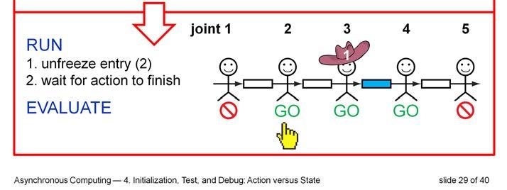
17 We are now ready to add GO control. We addgo control by adding ago control signalafter the AND gate, and we call that signal go. The gosignal comes with its own arbiter -the green box. so we can safely stop self-timed actions in full flight. The green box is called "Mister GO" (MrGO). Do you remember Ivan's talk about arbitration (part 3)? MrGOarbitrates between a low GO signal, to stop the action, and a high input signal coming from the AND gate, to continue the action. The arbiter either stops the action, if the low go signal wins, or it continues the action if the high AND signal wins. If the action continues because the high AND signal won the race, then the output of MrGOwill go low and its inversion used here will go high and the joint will drain in and fill out... and then it will self-reset. As soon as it self-resets, the AND gate will go low, and the go signal will grab the arbiter and stop the next action. MrGO is a non-blocking arbiter that's fair to the loser. To summarize: The green box is called "Mister GO" (MrGO). <CLICK> When gois high MrGOunfreezes the joint action, and allows it to run as usual. When gois low MrGOacts like a proper stopper and will stop and freeze the joint action safely. We use the scan chain to deliver the individual gosignals. 17

18 This is a transistor level implementation of MrGO. Do you recognize the arbiter circuit from Ivan's talk about arbiters? MrGOarbitrates between a high insignal to make outlow and a low GO signal to keep outhigh. 18


19 We have two working silicon experiments, called Weaver and Anvil. Both use links and joints with full-empty interfaces and MrGOwith an industry-standard JTAG scan interface for test, debug, and characterization. <CLICK for "MrGO approved" STAMP> Both the Weaver and Anvil have passed all tests that we, our students, and our visitors have thrown at them. 19
20 The proof of the pudding is in the eating. So, let's do a test. 20
21 Hereis a FIFO with 5 joints. Joint number 3 has a cowboy hat -that's a counter. We will test the counter at speed. We can do this in three steps, called Initialize, run, and evaluate. NOTE: for proper alignment,the text hasbeenhidden by making it white, and uncovered in the next few slides by making it black. 21
22 To initialize the system, we first freeze all the joints. We do this bymaking all the gosignals low as indicated by the red stop signs. We use a scan chain to initialize the go signals. Thiswillstopeveryaction in the FIFO. 22

23 Next, we setthe state. To run one DATA item through this FIFO, we make the first link full and the other links empty. We also set the counter. In this case, we choose to make the counter zero. Again, we use a scan chain to initialize the links and the counter. 23
24 Then we open the landing runway by unfreezing joints 3 and 4. Weuse a scan chain to set these two GO signals. 24
25 And that's our initial state. Notethat we kept the first and last joints frozen. This confines the test setup. Other test inputs cannot get in, and our test results cannot escape. 25
26 The test is now ready for take-off. We permit it to take off by making thego signal of joint number 2 high. That's the go signal at the hand-cursor. We call joint 2 "the gate keeper". We use the scan chain to enable this GO signal. As soon as the go signal at the hand-cursor is high, the data in the blue (full) link will make three moves, going left to right, and increase the counter value by 1. This will all happen at speed, without any interaction from me. At speed in this presentation is 1 second per move. It will take 3 seconds for the blue data to move from left to right. In the Weaver, which is 40nm CMOS, each move is ONLY 100 picoseconds. So the blue data will zip through in 300 picoseconds. Here we GO! 26
27 <SELF-TIMED> 27
28 <SELF-TIMED> 28
29 <SELF-TIMED> 29
30 <SELF-TIMED> 30
31 After 300 picoseconds, we scanthe counter data out to validate that it's now 1. AND SO IT IS!!! 31

32 We can easily extend the previous test to test a burst of data items at speed through the counter. 32


33 At the top-left, we set up a take-off runway with as many full links with data items as we want in the burst. At the top-right, we set up a landing runway with as many empty links as are needed to store the results generated in this test. As before, we kept the first and last joints in each runway frozen. to confine the test setup, so other test inputs cannot get in, and our test results cannot escape. Then we unfreeze the gate keeper, which is the joint with the handcursor. We let the circuit run its course, and then scan out the data captured by the landing runway. 33
34 Remember the canopy graphs that we use to characterize throughput? 34

35 Here is a reminder. These are the canopy graphs measured from the Weaver chip. We've seen them earlier in my talk about link and joint building blocks. The graphs show the throughput for the various ring-fifos in the Weaver. The horizontal axis shows the number of full links in the ring. The vertical axis shows the throughput measured as the number of GigaDataItems per second counted by each ring counter.

36 This is how we measure the throughput for those canopy graph: We initialize the ring counter to zero. We make ilinks full and the other links empty. We run the system by enabling the go signal of the gate-keeper. The gatekeeper is the joint at the yellow handcursor. After 1 second we disable that gosignal. Then we read out the counter value. The link-joint picture on the bottom of the slide shows that with 60% of the links full the ring counter counts 6 Giga Data Items in a single second. Let's go back to the canopy graph <GO BACK TO PREVIOUS SLIDE> See: the canopy graphs of the eight rings that go through the crossbar show a throughput of 6 Giga Data Items per second when the ring is 60% full, that is when of the links are full. <FORWARD TO THIS SLIDE> NOTE: no boundary joints here - only a gatekeeper, because the experiment is already contained by the ring. 36
37 Thereare a few rules to make MrGOand scan work together. The crux is to avoid interference between test and circuit operations. Informally, this boils down to: Don't scan the system when it's running, except to stop it. More formally, it's a good idea to (1)Stopthe actions in a joint before scanning statein or out of links that are used by those actions. (2)First change go signals that are being disabled before you enable go signals. (3) Use three separate scan chains for go,full-empty, and data. 37
38 38
39 I'd like to end by reminding everyone of our vision. The link-joint model with its full-empty protocol and with its local action-state control provides a clean and simple interface for hardware-software co-design-and-test. We want to use this clean and simple interface to enable computer scientists and electrical engineers to collaborate and to design and test -jointly -the systems of the future whose computations -we believe -will be distributed over space and time and will be of a self-timed nature. 39
40 40
ASYNC Naturalized Communication and Testing
 Naturalized communication and testing has been an amazing team builder. The ideas came out of the research work by the first three authors. and have been tested on silicon by the other three authors. You
Good afternoon! My name is Swetha Mettala Gilla you can call me Swetha.
 Good afternoon! My name is Swetha Mettala Gilla you can call me Swetha. I m a student at the Electrical and Computer Engineering Department and at the Asynchronous Research Center. This talk is about the
Digital Circuits 4: Sequential Circuits
 Digital Circuits 4: Sequential Circuits Created by Dave Astels Last updated on 2018-04-20 07:42:42 PM UTC Guide Contents Guide Contents Overview Sequential Circuits Onward Flip-Flops R-S Flip Flop Level
Computer Systems Architecture
 Computer Systems Architecture Fundamentals Of Digital Logic 1 Our Goal Understand Fundamentals and basics Concepts How computers work at the lowest level Avoid whenever possible Complexity Implementation
Section 24. Programming and Diagnostics
 Section. and Diagnostics HIGHLIGHTS This section of the manual contains the following topics:.1 Introduction... -2.2 In-Circuit Serial... -2.3 Enhanced In-Circuit Serial... -5.4 JTAG Boundary Scan... -6.5
Chapter 2. Digital Circuits
 Chapter 2. Digital Circuits Logic gates Flip-flops FF registers IC registers Data bus Encoders/Decoders Multiplexers Troubleshooting digital circuits Most contents of this chapter were covered in 88-217
Scan. This is a sample of the first 15 pages of the Scan chapter.
 Scan This is a sample of the first 15 pages of the Scan chapter. Note: The book is NOT Pinted in color. Objectives: This section provides: An overview of Scan An introduction to Test Sequences and Test
Section 24. Programming and Diagnostics
 Section. Programming and Diagnostics HIGHLIGHTS This section of the manual contains the following topics:.1 Introduction... -2.2 In-Circuit Serial Programming... -3.3 Enhanced In-Circuit Serial Programming...
Laboratory Exercise 4
 Laboratory Exercise 4 Polling and Interrupts The purpose of this exercise is to learn how to send and receive data to/from I/O devices. There are two methods used to indicate whether or not data can be
Experiment # 4 Counters and Logic Analyzer
 EE20L - Introduction to Digital Circuits Experiment # 4. Synopsis: Experiment # 4 Counters and Logic Analyzer In this lab we will build an up-counter and a down-counter using 74LS76A - Flip Flops. The
Based on slides/material by. Topic 14. Testing. Testing. Logic Verification. Recommended Reading:
 Based on slides/material by Topic 4 Testing Peter Y. K. Cheung Department of Electrical & Electronic Engineering Imperial College London!! K. Masselos http://cas.ee.ic.ac.uk/~kostas!! J. Rabaey http://bwrc.eecs.berkeley.edu/classes/icbook/instructors.html
Raspberry Pi debugging with JTAG
 Arseny Kurnikov Aalto University December 13, 2013 Outline JTAG JTAG on RPi Linux kernel debugging JTAG Joint Test Action Group is a standard for a generic transport interface for integrated circuits.
Using the XC9500/XL/XV JTAG Boundary Scan Interface
 Application Note: XC95/XL/XV Family XAPP69 (v3.) December, 22 R Using the XC95/XL/XV JTAG Boundary Scan Interface Summary This application note explains the XC95 /XL/XV Boundary Scan interface and demonstrates
COE328 Course Outline. Fall 2007
 COE28 Course Outline Fall 2007 1 Objectives This course covers the basics of digital logic circuits and design. Through the basic understanding of Boolean algebra and number systems it introduces the student
LAX_x Logic Analyzer
 Legacy documentation LAX_x Logic Analyzer Summary This core reference describes how to place and use a Logic Analyzer instrument in an FPGA design. Core Reference CR0103 (v2.0) March 17, 2008 The LAX_x
Overview of BDM nc. The IEEE JTAG specification is also recommended reading for those unfamiliar with JTAG. 1.2 Overview of BDM Before the intr
 Application Note AN2387/D Rev. 0, 11/2002 MPC8xx Using BDM and JTAG Robert McEwan NCSD Applications East Kilbride, Scotland As the technical complexity of microprocessors has increased, so too has the
Digital Systems Laboratory 3 Counters & Registers Time 4 hours
 Digital Systems Laboratory 3 Counters & Registers Time 4 hours Aim: To investigate the counters and registers constructed from flip-flops. Introduction: In the previous module, you have learnt D, S-R,
EECS150 - Digital Design Lecture 10 - Interfacing. Recap and Topics
 EECS150 - Digital Design Lecture 10 - Interfacing Oct. 1, 2013 Prof. Ronald Fearing Electrical Engineering and Computer Sciences University of California, Berkeley (slides courtesy of Prof. John Wawrzynek)
IT T35 Digital system desigm y - ii /s - iii
 UNIT - III Sequential Logic I Sequential circuits: latches flip flops analysis of clocked sequential circuits state reduction and assignments Registers and Counters: Registers shift registers ripple counters
Chapter 6. Flip-Flops and Simple Flip-Flop Applications
 Chapter 6 Flip-Flops and Simple Flip-Flop Applications Basic bistable element It is a circuit having two stable conditions (states). It can be used to store binary symbols. J. C. Huang, 2004 Digital Logic
EE178 Spring 2018 Lecture Module 5. Eric Crabill
 EE178 Spring 2018 Lecture Module 5 Eric Crabill Goals Considerations for synchronizing signals Clocks Resets Considerations for asynchronous inputs Methods for crossing clock domains Clocks The academic
Digital Fundamentals: A Systems Approach
 Digital Fundamentals: A Systems Approach Counters Chapter 8 A System: Digital Clock Digital Clock: Counter Logic Diagram Digital Clock: Hours Counter & Decoders Finite State Machines Moore machine: One
CSE 352 Laboratory Assignment 3
 CSE 352 Laboratory Assignment 3 Introduction to Registers The objective of this lab is to introduce you to edge-trigged D-type flip-flops as well as linear feedback shift registers. Chapter 3 of the Harris&Harris
CS8803: Advanced Digital Design for Embedded Hardware
 CS883: Advanced Digital Design for Embedded Hardware Lecture 4: Latches, Flip-Flops, and Sequential Circuits Instructor: Sung Kyu Lim (limsk@ece.gatech.edu) Website: http://users.ece.gatech.edu/limsk/course/cs883
Sequential Digital Design. Laboratory Manual. Experiment #7. Counters
 The Islamic University of Gaza Engineering Faculty Department of Computer Engineering Spring 2018 ECOM 2022 Khaleel I. Shaheen Sequential Digital Design Laboratory Manual Experiment #7 Counters Objectives
Synchronization in Asynchronously Communicating Digital Systems
 Synchronization in Asynchronously Communicating Digital Systems Priyadharshini Shanmugasundaram Abstract Two digital systems working in different clock domains require a protocol to communicate with each
Table of Contents Introduction
 Page 1/9 Waveforms 2015 tutorial 3-Jan-18 Table of Contents Introduction Introduction to DAD/NAD and Waveforms 2015... 2 Digital Functions Static I/O... 2 LEDs... 2 Buttons... 2 Switches... 2 Pattern Generator...
EE178 Lecture Module 4. Eric Crabill SJSU / Xilinx Fall 2005
 EE178 Lecture Module 4 Eric Crabill SJSU / Xilinx Fall 2005 Lecture #9 Agenda Considerations for synchronizing signals. Clocks. Resets. Considerations for asynchronous inputs. Methods for crossing clock
EE241 - Spring 2001 Advanced Digital Integrated Circuits. References
 EE241 - Spring 2001 Advanced Digital Integrated Circuits Lecture 28 References Rabaey, Digital Integrated Circuits and EE241 (1998) notes Chapter 25, ing of High-Performance Processors by D.K. Bhavsar
Laboratory 1 - Introduction to Digital Electronics and Lab Equipment (Logic Analyzers, Digital Oscilloscope, and FPGA-based Labkit)
") Massachusetts Institute of Technology Department of Electrical Engineering and Computer Science 6. - Introductory Digital Systems Laboratory (Spring 006) Laboratory - Introduction to Digital Electronics
Massachusetts Institute of Technology Department of Electrical Engineering and Computer Science 6. - Introductory Digital Systems Laboratory (Spring 006) Laboratory - Introduction to Digital Electronics
Lecture 8: Sequential Logic
 Lecture 8: Sequential Logic Last lecture discussed how we can use digital electronics to do combinatorial logic we designed circuits that gave an immediate output when presented with a given set of inputs
EXPERIMENT #6 DIGITAL BASICS
 EXPERIMENT #6 DIGITL SICS Digital electronics is based on the binary number system. Instead of having signals which can vary continuously as in analog circuits, digital signals are characterized by only
Asynchronous (Ripple) Counters
 Counters") Circuits for counting events are frequently used in computers and other digital systems. Since a counter circuit must remember its past states, it has to possess memory. The chapter about flip-flops introduced
Circuits for counting events are frequently used in computers and other digital systems. Since a counter circuit must remember its past states, it has to possess memory. The chapter about flip-flops introduced
Review of digital electronics. Storage units Sequential circuits Counters Shifters
 Review of digital electronics Storage units Sequential circuits ounters Shifters ounting in Binary A counter can form the same pattern of 0 s and 1 s with logic levels. The first stage in the counter represents
3/5/2017. A Register Stores a Set of Bits. ECE 120: Introduction to Computing. Add an Input to Control Changing a Register s Bits
 University of Illinois at Urbana-Champaign Dept. of Electrical and Computer Engineering ECE 120: Introduction to Computing Registers A Register Stores a Set of Bits Most of our representations use sets
Logic. Andrew Mark Allen March 4, 2012
 Logic Andrew Mark Allen - 05370299 March 4, 2012 Abstract NAND gates and inverters were used to construct several different logic gates whose operations were investigate under various inputs. Then the
Physics 217A LAB 4 Spring 2016 Shift Registers Tri-State Bus. Part I
 Physics 217A LAB 4 Spring 2016 Shift Registers Tri-State Bus Part I 0. In this part of the lab you investigate the 164 a serial-in, 8-bit-parallel-out, shift register. 1. Press in (near the LEDs) a 164.
Design and Simulation of a Digital CMOS Synchronous 4-bit Up-Counter with Set and Reset
 Design and Simulation of a Digital CMOS Synchronous 4-bit Up-Counter with Set and Reset Course Number: ECE 533 Spring 2013 University of Tennessee Knoxville Instructor: Dr. Syed Kamrul Islam Prepared by
A video signal processor for motioncompensated field-rate upconversion in consumer television
 A video signal processor for motioncompensated field-rate upconversion in consumer television B. De Loore, P. Lippens, P. Eeckhout, H. Huijgen, A. Löning, B. McSweeney, M. Verstraelen, B. Pham, G. de Haan,
MUHAMMAD NAEEM LATIF MCS 3 RD SEMESTER KHANEWAL
 1. A stage in a shift register consists of (a) a latch (b) a flip-flop (c) a byte of storage (d) from bits of storage 2. To serially shift a byte of data into a shift register, there must be (a) one click
COMP2611: Computer Organization. Introduction to Digital Logic
 1 COMP2611: Computer Organization Sequential Logic Time 2 Till now, we have essentially ignored the issue of time. We assume digital circuits: Perform their computations instantaneously Stateless: once
55:131 Introduction to VLSI Design Project #1 -- Fall 2009 Counter built from NAND gates, timing Due Date: Friday October 9, 2009.
 55:131 Introduction to VLSI Design Project #1 -- Fall 2009 Counter built from NAND gates, timing Due Date: Friday October 9, 2009 Introduction In this project we will create a transistor-level model of
Advanced Devices. Registers Counters Multiplexers Decoders Adders. CSC258 Lecture Slides Steve Engels, 2006 Slide 1 of 20
 Advanced Devices Using a combination of gates and flip-flops, we can construct more sophisticated logical devices. These devices, while more complex, are still considered fundamental to basic logic design.
CHAPTER 4: Logic Circuits
 CHAPTER 4: Logic Circuits II. Sequential Circuits Combinational circuits o The outputs depend only on the current input values o It uses only logic gates, decoders, multiplexers, ALUs Sequential circuits
UNIT IV CMOS TESTING. EC2354_Unit IV 1
 UNIT IV CMOS TESTING EC2354_Unit IV 1 Outline Testing Logic Verification Silicon Debug Manufacturing Test Fault Models Observability and Controllability Design for Test Scan BIST Boundary Scan EC2354_Unit
Notes on Digital Circuits
 PHYS 331: Junior Physics Laboratory I Notes on Digital Circuits Digital circuits are collections of devices that perform logical operations on two logical states, represented by voltage levels. Standard
Previous Lecture Sequential Circuits. Slide Summary of contents covered in this lecture. (Refer Slide Time: 01:55)
") Previous Lecture Sequential Circuits Digital VLSI System Design Prof. S. Srinivasan Department of Electrical Engineering Indian Institute of Technology, Madras Lecture No 7 Sequential Circuit Design Slide
Previous Lecture Sequential Circuits Digital VLSI System Design Prof. S. Srinivasan Department of Electrical Engineering Indian Institute of Technology, Madras Lecture No 7 Sequential Circuit Design Slide
Experiment 8 Introduction to Latches and Flip-Flops and registers
 Experiment 8 Introduction to Latches and Flip-Flops and registers Introduction: The logic circuits that have been used until now were combinational logic circuits since the output of the device depends
Introduction. NAND Gate Latch. Digital Logic Design 1 FLIP-FLOP. Digital Logic Design 1
 2007 Introduction BK TP.HCM FLIP-FLOP So far we have seen Combinational Logic The output(s) depends only on the current values of the input variables Here we will look at Sequential Logic circuits The
Chenguang Guo, Lei Chen, and Yanlong Zhang
 International Journal of Electronics and Electrical Engineering 6 22 Chenguang Guo, Lei Chen, and Yanlong Zhang Abstract This paper describes a novel optimized JTAG interface circuit between a JTAG controller
Laboratory 9 Digital Circuits: Flip Flops, One-Shot, Shift Register, Ripple Counter
 page 1 of 5 Digital Circuits: Flip Flops, One-Shot, Shift Register, Ripple Counter Introduction In this lab, you will learn about the behavior of the D flip-flop, by employing it in 3 classic circuits:
Microcontrollers and Interfacing week 7 exercises
 SERIL TO PRLLEL CONVERSION Serial to parallel conversion Microcontrollers and Interfacing week exercises Using many LEs (e.g., several seven-segment displays or bar graphs) is difficult, because only a
Counter dan Register
 Counter dan Register Introduction Circuits for counting events are frequently used in computers and other digital systems. Since a counter circuit must remember its past states, it has to possess memory.
Topics. Microelectronics Revolution. Digital Circuits Part 1 Logic Gates. Introductory Medical Device Prototyping
 Introductory Medical Device Prototyping Digital Circuits Part 1 Logic Gates, http://saliterman.umn.edu/ Department of Biomedical Engineering, University of Minnesota Topics Digital Electronics CMOS Logic
Spiral Content Mapping. Spiral 2 1. Learning Outcomes DATAPATH COMPONENTS. Datapath Components: Counters Adders Design Example: Crosswalk Controller
 -. -. piral Content Mapping piral Theory Combinational Design equential Design ystem Level Design Implementation and Tools Project piral Performance metrics (latency vs. throughput) Boolean Algebra Canonical
Logic Design. Flip Flops, Registers and Counters
 Logic Design Flip Flops, Registers and Counters Introduction Combinational circuits: value of each output depends only on the values of inputs Sequential Circuits: values of outputs depend on inputs and
Instructions. Final Exam CPSC/ELEN 680 December 12, Name: UIN:
 Final Exam CPSC/ELEN 680 December 12, 2005 Name: UIN: Instructions This exam is closed book. Provide brief but complete answers to the following questions in the space provided, using figures as necessary.
Figure 9.1: A clock signal.
 Chapter 9 Flip-Flops 9.1 The clock Synchronous circuits depend on a special signal called the clock. In practice, the clock is generated by rectifying and amplifying a signal generated by special non-digital
VTU NOTES QUESTION PAPERS NEWS RESULTS FORUMS Registers
 Registers Registers are a very important digital building block. A data register is used to store binary information appearing at the output of an encoding matrix.shift registers are a type of sequential
VLSI Test Technology and Reliability (ET4076)
") VLSI Test Technology and Reliability (ET476) Lecture 9 (2) Built-In-Self Test (Chapter 5) Said Hamdioui Computer Engineering Lab Delft University of Technology 29-2 Learning aims Describe the concept and
VLSI Test Technology and Reliability (ET476) Lecture 9 (2) Built-In-Self Test (Chapter 5) Said Hamdioui Computer Engineering Lab Delft University of Technology 29-2 Learning aims Describe the concept and
We are here. Assembly Language. Processors Arithmetic Logic Units. Finite State Machines. Circuits Gates. Transistors
 CSC258 Week 5 1 We are here Assembly Language Processors Arithmetic Logic Units Devices Finite State Machines Flip-flops Circuits Gates Transistors 2 Circuits using flip-flops Now that we know about flip-flops
EE 367 Lab Part 1: Sequential Logic
 EE367: Introduction to Microprocessors Section 1.0 EE 367 Lab Part 1: Sequential Logic Contents 1 Preface 1 1.1 Things you need to do before arriving in the Laboratory............... 2 1.2 Summary of material
Digital Blocks Semiconductor IP
 Digital Blocks Semiconductor IP General Description The Digital Blocks core is a full function equivalent to the Motorola MC6845 device. The interfaces a microprocessor to a raster-scan CRT display. The
How to overcome/avoid High Frequency Effects on Debug Interfaces Trace Port Design Guidelines
 How to overcome/avoid High Frequency Effects on Debug Interfaces Trace Port Design Guidelines An On-Chip Debugger/Analyzer (OCD) like isystem s ic5000 (Figure 1) acts as a link to the target hardware by
Other Flip-Flops. Lecture 27 1
 Other Flip-Flops Other types of flip-flops can be constructed by using the D flip-flop and external logic. Two flip-flops less widely used in the design of digital systems are the JK and T flip-flops.
16 Dec Testing and Programming PCBA s. 1 JTAG Technologies
 6 Dec 24 Testing and Programming PCBA s JTAG Technologies The importance of Testing Don t ship bad products to your customers, find problems before they do. DOA s (Death On Arrival) lead to huge costs
Simulation Mismatches Can Foul Up Test-Pattern Verification
 1 of 5 12/17/2009 2:59 PM Technologies Design Hotspots Resources Shows Magazine ebooks & Whitepapers Jobs More... Click to view this week's ad screen [ D e s i g n V i e w / D e s i g n S o lu ti o n ]
CHAPTER 4: Logic Circuits
 CHAPTER 4: Logic Circuits II. Sequential Circuits Combinational circuits o The outputs depend only on the current input values o It uses only logic gates, decoders, multiplexers, ALUs Sequential circuits
Objectives. Combinational logics Sequential logics Finite state machine Arithmetic circuits Datapath
 Objectives Combinational logics Sequential logics Finite state machine Arithmetic circuits Datapath In the previous chapters we have studied how to develop a specification from a given application, and
Comparing JTAG, SPI, and I2C
 Comparing JTAG, SPI, and I2C Application by Russell Hanabusa 1. Introduction This paper discusses three popular serial buses: JTAG, SPI, and I2C. A typical electronic product today will have one or more
JRC ( JTAG Route Controller ) Data Sheet
 Data Sheet") JRC ( JTAG Route Controller ) Data Sheet ATLAS TGC Electronics Group September 5, 2002 (version 1.1) Author : Takashi Takemoto Feature * JTAG signal router with two inputs and seven outputs. * Routing
JRC ( JTAG Route Controller ) Data Sheet ATLAS TGC Electronics Group September 5, 2002 (version 1.1) Author : Takashi Takemoto Feature * JTAG signal router with two inputs and seven outputs. * Routing
EE241 - Spring 2005 Advanced Digital Integrated Circuits
 EE241 - Spring 2005 Advanced Digital Integrated Circuits Lecture 21: Asynchronous Design Synchronization Clock Distribution Self-Timed Pipelined Datapath Req Ack HS Req Ack HS Req Ack HS Req Ack Start
CPSC 121: Models of Computation Lab #5: Flip-Flops and Frequency Division
 CPSC 121: Models of Computation Lab #5: Flip-Flops and Frequency Division Objectives In this lab, we will see the sequential circuits latches and flip-flops. Latches and flip-flops can be used to build
Name Of The Experiment: Sequential circuit design Latch, Flip-flop and Registers
 EEE 304 Experiment No. 07 Name Of The Experiment: Sequential circuit design Latch, Flip-flop and Registers Important: Submit your Prelab at the beginning of the lab. Prelab 1: Construct a S-R Latch and
Fundamentals of Computer Systems
 Fundamentals of Computer Systems Sequential Logic Stephen A. Edwards Columbia University Fall 2012 State-Holding Elements Bistable Elements Equivalent circuits; right is more traditional. Two stable states:
ECE 270 Lab Verification / Evaluation Form. Experiment 9
 ECE 270 Lab Verification / Evaluation Form Experiment 9 Evaluation: IMPORTANT! You must complete this experiment during your scheduled lab period. All work for this experiment must be demonstrated to and
(Refer Slide Time: 1:45)
") (Refer Slide Time: 1:45) Digital Circuits and Systems Prof. S. Srinivasan Department of Electrical Engineering Indian Institute of Technology, Madras Lecture - 30 Encoders and Decoders So in the last lecture
(Refer Slide Time: 1:45) Digital Circuits and Systems Prof. S. Srinivasan Department of Electrical Engineering Indian Institute of Technology, Madras Lecture - 30 Encoders and Decoders So in the last lecture
Logic and Computer Design Fundamentals. Chapter 7. Registers and Counters
 Logic and Computer Design Fundamentals Chapter 7 Registers and Counters Registers Register a collection of binary storage elements In theory, a register is sequential logic which can be defined by a state
Lab #5: Design Example: Keypad Scanner and Encoder - Part 1 (120 pts)
") Nate Pihlstrom, npihlstr@uccs.edu Lab #5: Design Example: Keypad Scanner and Encoder - Part 1 (120 pts) Objective The objective of lab assignments 5 through 9 are to systematically design and implement
Nate Pihlstrom, npihlstr@uccs.edu Lab #5: Design Example: Keypad Scanner and Encoder - Part 1 (120 pts) Objective The objective of lab assignments 5 through 9 are to systematically design and implement
Digital Circuits I and II Nov. 17, 1999
 Physics 623 Digital Circuits I and II Nov. 17, 1999 Digital Circuits I 1 Purpose To introduce the basic principles of digital circuitry. To understand the small signal response of various gates and circuits
Random Access Scan. Veeraraghavan Ramamurthy Dept. of Electrical and Computer Engineering Auburn University, Auburn, AL
 Random Access Scan Veeraraghavan Ramamurthy Dept. of Electrical and Computer Engineering Auburn University, Auburn, AL ramamve@auburn.edu Term Paper for ELEC 7250 (Spring 2005) Abstract: Random Access
PARALLEL PROCESSOR ARRAY FOR HIGH SPEED PATH PLANNING
 PARALLEL PROCESSOR ARRAY FOR HIGH SPEED PATH PLANNING S.E. Kemeny, T.J. Shaw, R.H. Nixon, E.R. Fossum Jet Propulsion LaboratoryKalifornia Institute of Technology 4800 Oak Grove Dr., Pasadena, CA 91 109
Product Update. JTAG Issues and the Use of RT54SX Devices
 Product Update Revision Date: September 2, 999 JTAG Issues and the Use of RT54SX Devices BACKGROUND The attached paper authored by Richard B. Katz of NASA GSFC and J. J. Wang of Actel describes anomalies
Topic D-type Flip-flops. Draw a timing diagram to illustrate the significance of edge
 Topic 1.3.2 -type Flip-flops. Learning Objectives: At the end of this topic you will be able to; raw a timing diagram to illustrate the significance of edge triggering; raw a timing diagram to illustrate
Universal Asynchronous Receiver- Transmitter (UART)
") Universal Asynchronous Receiver- Transmitter (UART) (UART) Block Diagram Four-Bit Bidirectional Shift Register Shift Register Counters Shift registers can form useful counters by recirculating a pattern
Universal Asynchronous Receiver- Transmitter (UART) (UART) Block Diagram Four-Bit Bidirectional Shift Register Shift Register Counters Shift registers can form useful counters by recirculating a pattern
Computer Organization
 Computer Organization Douglas Comer Computer Science Department Purue University 25 N. University Street West Lafayette, IN 4797-266 http://www.cs.purue.eu/people/comer Copyright 26. All rights reserve.
18 Nov 2015 Testing and Programming PCBA s. 1 JTAG Technologies
 8 Nov 25 Testing and Programming PCBA s JTAG Technologies The importance of Testing Don t ship bad products to your customers, find problems before they do. DOA s (Death On Arrival) lead to huge costs
Registers and Counters
 Registers and Counters A register is a group of flip-flops which share a common clock An n-bit register consists of a group of n flip-flops capable of storing n bits of binary information May have combinational
Programmable Logic Design I
 Programmable Logic Design I Introduction In labs 11 and 12 you built simple logic circuits on breadboards using TTL logic circuits on 7400 series chips. This process is simple and easy for small circuits.
LSN 12 Shift Registers
 LSN 12 Shift Registers Department of Engineering Technology LSN 12 Shift Registers Digital circuits with data storage and data movement functions Storage capacity is the total number of bits of digital
Chapter 4: One-Shots, Counters, and Clocks
 Chapter 4: One-Shots, Counters, and Clocks I. The Monostable Multivibrator (One-Shot) The timing pulse is one of the most common elements of laboratory electronics. Pulses can control logical sequences
Y. Tsiatouhas. VLSI Systems and Computer Architecture Lab. Boundary Scan (JTAG ) 2
 2") CMOS INTEGRATE CIRCUIT EGN TECHNIUES University of Ioannina Boundary Scan Testing (JTAG ΙΕΕΕ 49 std) ept of Computer Science and Engineering Y Tsiatouhas CMOS Integrated Circuit esign Techniques VL Systems
CMOS INTEGRATE CIRCUIT EGN TECHNIUES University of Ioannina Boundary Scan Testing (JTAG ΙΕΕΕ 49 std) ept of Computer Science and Engineering Y Tsiatouhas CMOS Integrated Circuit esign Techniques VL Systems
3. Configuration and Testing
 3. Configuration and Testing C51003-1.4 IEEE Std. 1149.1 (JTAG) Boundary Scan Support All Cyclone devices provide JTAG BST circuitry that complies with the IEEE Std. 1149.1a-1990 specification. JTAG boundary-scan
Testing Digital Systems II
 Testing Digital Systems II Lecture 2: Design for Testability (I) structor: M. Tahoori Copyright 2010, M. Tahoori TDS II: Lecture 2 1 History During early years, design and test were separate The final
(Refer Slide Time: 2:00)
") Digital Circuits and Systems Prof. Dr. S. Srinivasan Department of Electrical Engineering Indian Institute of Technology, Madras Lecture #21 Shift Registers (Refer Slide Time: 2:00) We were discussing
Digital Circuits and Systems Prof. Dr. S. Srinivasan Department of Electrical Engineering Indian Institute of Technology, Madras Lecture #21 Shift Registers (Refer Slide Time: 2:00) We were discussing
Lecture 17: Introduction to Design For Testability (DFT) & Manufacturing Test
 & Manufacturing Test") Lecture 17: Introduction to Design For Testability (DFT) & Manufacturing Test Mark McDermott Electrical and Computer Engineering The University of Texas at Austin Agenda Introduction to testing Logical
Lecture 17: Introduction to Design For Testability (DFT) & Manufacturing Test Mark McDermott Electrical and Computer Engineering The University of Texas at Austin Agenda Introduction to testing Logical
Registers and Counters
 Registers and Counters Clocked sequential circuit = F/Fs and combinational gates Register Group of flip-flops (share a common clock and capable of storing one bit of information) Consist of a group of
PICOSECOND TIMING USING FAST ANALOG SAMPLING
 PICOSECOND TIMING USING FAST ANALOG SAMPLING H. Frisch, J-F Genat, F. Tang, EFI Chicago, Tuesday 6 th Nov 2007 INTRODUCTION In the context of picosecond timing, analog detector pulse sampling in the 10
Sharif University of Technology. SoC: Introduction
 SoC Design Lecture 1: Introduction Shaahin Hessabi Department of Computer Engineering System-on-Chip System: a set of related parts that act as a whole to achieve a given goal. A system is a set of interacting
Logic Analyzer Auto Run / Stop Channels / trigger / Measuring Tools Axis control panel Status Display
 Logic Analyzer The graphical user interface of the Logic Analyzer fits well into the overall design of the Red Pitaya applications providing the same operating concept. The Logic Analyzer user interface