ARM JTAG Interface Specifications
|
|
|
- Adelia Phillips
- 6 years ago
- Views:
Transcription
1 ARM JTAG Interface Specifications TRACE32 Online Help TRACE32 Directory TRACE32 Index TRACE32 Documents... ICD In-Circuit Debugger... Processor Architecture Manuals... ARM/CORTEX/XSCALE... ARM Application Notes... ARM JTAG Interface Specifications... 1 Introduction... 2 Mechanical Connector... 3 Signals... 4 DC Electrical Characteristics... 8 AC Timing Characteristics Debug Cable Driver/Receiver Output Circuitry 11 Input Circuitry 11 Target System Design Consideration Electrical 12 Example for Interface on Target Board 13 Layout Considerations 13 Reset Considerations Adaptive Clocking (Return Test Clock RTCK) Hot Plug-in Alternative Connector Types Mictor Half Size 20 TI ARM TI-20 Compact 23 MIPI-10/20/34, ARM-10/20 24 Debug Cable Hardware Versions ARM JTAG Interface Specifications 1
 to the JTAG connector on the target board.")
2 ARM JTAG Interface Specifications Version 06-Nov Aug-15 Changed the file name from arm_app_jtag.pdf to app_arm_jtag.pdf. Introduction The debugger communicates with the target processor via JTAG interface. It is connected with a probe cable (debug cable ) to the JTAG connector on the target board. This application note outlines the requirements to make the interface compatible with the LAUTERBACH debugger for ARM and XScale cores. It describes the requirements with respect to logical functionality, physical connector, electrical characteristics, timing behavior, and printed circuit board (PCB) design. It will be useful for target board designers and for engineers suspecting an issue in an existing interface. The following text assumes a debug cable version V3 (September 2003 or later) and the connector type of standard delivery. The chapter Debug Cable Hardware Versions describes the main differences to other versions. The chapter Alternative Connector Types lists optional connectors and available adapters. ARM JTAG Interface Specifications 2
 TRST- 3 4 GND TDI 5 6 GND TMS 7 8 GND TCK 9 10 GND RTCK 11 12 GND TDO 13 14 GND SRST- 15 16 GND DBGRQ 17 18 GND DBGACK 19 20 GND On the target board a male standard 20-pin")
 and a center polarization is recommended. These connectors, especially the headers without housing are available from many connector manufacturers.")
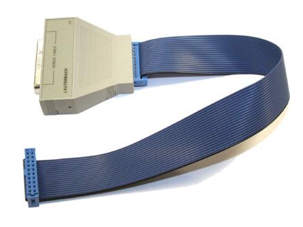
3 Mechanical Connector The mechanical connector is specified by ARM (ARM-20). VTREF 1 2 VSUPPLY(not used) TRST- 3 4 GND TDI 5 6 GND TMS 7 8 GND TCK 9 10 GND RTCK GND TDO GND SRST GND DBGRQ GND DBGACK GND On the target board a male standard 20-pin double row connector (two rows of ten pins), pin to pin spacing: in. x in., pin width in. square post is required. A connector with housing (shrouded) and a center polarization is recommended. These connectors, especially the headers without housing are available from many connector manufacturers. Examples with housing: Samtec: HTST L-D (through-hole) Samtec: HTST L-DV (surface mount) Examples without housing: Samtec: TSW L-D Berg: H Debug Cable Target Connector The connector of the debug cable mounted on the blue ribbon cable is an IDC female polarized socket connector of type Tyco / T&B: / ARM JTAG Interface Specifications 3
4 Signals This JTAG interface is a superset of IEEE Std TCK, TMS, TDI, TDO, TRST- are the standard JTAG signals. A few more signals are added for advanced debug capabilities. Signal Pin Description Direction (debugger point of view) Compliance VTREF 1 Voltage Reference is the target reference voltage. It indicates if the target power is applied, it is used to create the logic-level reference (VTREF/2) for the debugger input comparators and it auto adjusts the voltage levels of the debugger output driver. It shall be directly connected to the power supply of the processors IO pins. It might have a series resistor, although this is not recommended. It has to be strong enough to overdrive the 100 k pull-down resistor of the debug cable. VSUPPLY 2 Voltage Supply is used by some debug tools to draw it's supply current. This is not used (not connected) by LAUTERBACH tools which are all self-powered. You might connect this signal to a 5 V or 3.3 V power supply (no series resistor) which is able to supply power to non- LAUTERBACH debug tools. input input required not used ARM JTAG Interface Specifications 4
5 Signal Pin Description Direction (debugger point of view) Compliance TRST- 3 Test Reset (low active) is used for an asynchronous reset of the JTAG Test Access Port (TAP). It resets the TAP state machine and on most ARM families the debug register. See important notes in the chapter Reset Considerations. The debugger drives it by a push-pull driver. From the debugger point of view it is optional, because it resets the TAP also by a certain JTAG sequence. You should place a pull-down resistor (1 k - 47 k ) on this signal on target side, although this is not JTAG conform. It ensures the on-chip debug logic is inactive when the debugger is not connected. TDI 5 Test Data In is the data signal from debugger to processor. You can place a pull-up or pull-down resistor (1 k - 47 k ) on this line to ensure a defined state even when the line is not driven by the debugger. TMS 7 Test Mode Select is the control signal for the TAP controller. You can place a pull-up or pull-down resistor (1 k - 47 k ) on this line in order to give it a defined state even when the line is not driven by the debugger. TCK 9 Test Clock is the clock signal from debugger to processor. You should place a pull-up or pull-down resistor (1 k - 47 k ) on this line in order to give it a defined state even when the line is not driven by the debugger. output output output output optional required required required ARM JTAG Interface Specifications 5
6 Signal Pin Description Direction (debugger point of view) Compliance RTCK 11 Return Test Clock can be used to synchronize the JTAG signals to internal clocks. For more details see chapter Adaptive Clocking. If this is not required, then it can be used to compensate the propagation delays on driver and cable. This allows to reach higher JTAG clock frequencies. Therefore you need to feed-back the TCK signal buffered or unbuffered to this line. On an unbuffered feed-back it might have negative effect on signal reflection. Better provide a chance to cut the connection on the target (jumper or solder bridge) in case problems arise. TDO 13 Test Data Out is the data signal from processor to debugger. You can place a 33 series resistor close to the processor for series termination. You can place a pull-up or pull-down resistor (1 k - 47 k ) on this line. SRST- 15 System Reset (low active) is used to reset the target system. See important notes in the chapter Reset Considerations. The signal is also used by the debugger to detect if the processor is held in reset. There is no need to provide this indication, but if a reset condition is not signalized by this line it should be high (= no reset). The debugger drives it open-drain. A 47 k pull-up is within the debug cable. There might be the need to place a pull-up (1 k - 47 k ) on target side to avoid unintentional resets when the debugger is not connected and probably to strengthen the weak 47 k pull-up in the debug cable. input input input/ output optional required optional (require d for XSCAL E cores) ARM JTAG Interface Specifications 6
7 Signal Pin Description Direction (debugger point of view) Compliance DBGRQ 17 Debug Request (high active) is an output of the debugger to cause the processor to enter debug mode (to halt the processor). The debugger can send a debug request also in another way which is just slower. On many chips this signal is not provided externally. If available it can be used for fast stopping the processor with a hardware trigger e.g. for synchronous halt of all cores in a multicore system. If this signal is provided by the processor you should place a pull-down resistor (1 k - 47 k ) on target side for the case the debugger is not connected. DBGACK 19 Debug Acknowledge (high active) is an input of the debugger to sense the processors halt status. On many chips this signal is not provided externally. If available it can be used for fast triggering e.g. for synchronous halt of all cores in a multicore system. output input optional optional GND 4, 6, 8, 10, 12, 14, 16, 18, (20) Ground. All pins should be connected to minimize noise pickup. In the debug cable Pin 20 is connected to ground via a 100 resistor to avoid damage of the debug cable in case it will be connected inversely. required There is an additional, small gold plug on the side of the debug cable case. This signal is not required. It can be used for customer specific solutions. ARM JTAG Interface Specifications 7
8 DC Electrical Characteristics The table below describes the DC electrical characteristics at the 20-pin JTAG connector of the debug cable. The values for current measures positive in direction from the debug cable to the target system. The characteristics apply to the full operation range of the target system. The values below are for reference only and are not guaranteed by LAUTERBACH. Symbol Vvtref Vvtref_ pwrdwn Ivtref Description VTREF operating voltage VTREF power down indication VTREF current Condition Min. Typ. Max. Unit V V Vvtref = 5.25V ma Vil Low-level input voltage Vvtref = 1.5V Vvtref = 1.8V Vvtref = 2.5V Vvtref = 3.3V Vvtref = 5.0V * Vvtref V Vih High-level input voltage Vvtref = 1.5V Vvtref = 1.8V Vvtref = 2.5V Vvtref = 3.3V Vvtref = 5.0V 0.7 * Vvtref V Vol Low-level output voltage typ. values for: Iol = -0.1mA Iol = -1.6mA Iol = -6mA * Vvtref V Voh High-level output voltage (1) Vvtref = 0.4V Vvtref = 1.5V Vvtref = 1.8V Vvtref = 2.5V Vvtref = 3.3V Vvtref = 5.0V 0.4V: Ioh=2mA other: Ioh=6mA 0.7* Vvtref Vvtref V ARM JTAG Interface Specifications 8
9 Symbol Iil Iih Description Low-level input current High-level input current Condition Min. Typ. Max. Unit 0.2 ma -0.2 ma Iol Low-level output current Vvtref < 1.5V Vvtref >= 1.5V Vol < 0.3*Vvtref -2-6 ma Ioh High-level output current (1) Vvtref < 1.5V Vvtref >= 1.5V Voh > 0.7*Vvtref 2 6 ma (1) except SRST- which is driven open-drain. There is a 47 k pull-up in the debug cable. An additional pull-up on target side might be required. ARM JTAG Interface Specifications 9
10 AC Timing Characteristics Important for the timing is that the data on TDI and TMS will be sampled with the rising edge of TCK (will be output on the falling edge) and that TDO will change on the falling edge of TCK (exception see Adaptive Clocking). All delays will affect the maximum possible JTAG frequency (TCK) which is selectable in the LAUTERBACH tool (default setting: 10 MHz). Issues with minimal setup and hold times can always be resolved by simply decreasing the TCK frequency, because this increases the separation between signal changing and being sampled. Nether the less you should minimize the delays in order to get a good performance e.g. when downloading the application program by the debugger. The following table should give you an example for the timing considerations in case you like to work with a 20 MHz JTAG clock frequency, which results in a very good performance. The timing is measured at the JTAG connector of the debug cable. Setup times and hold times are measured with respect to 50% signal level value, rise and fall times are measured at 20% and 80%. The measured values are for reference only and are not guaranteed by LAUTERBACH. Symbol Description Min. Max. Unit Ttck_high TCK high time ns Ttck_low TCK low time ns Tsetup TDI, TMS setup time before rising TCK 21 ns Thold TDI, TMS hold time after rising TCK 21 ns Ttdo_out TDO output delay time from falling TCK 0 16 ns Ttrst_low TRST- low time 1 ms Tsrst_low SRST- low time 1 ms Trf output rise / fall time load = 10 pf load = 22 pf load = 33 pf ns Values in table for 20 MHz JTAG clock (TCK). ARM JTAG Interface Specifications 10
11 Debug Cable Driver/Receiver This chapter describes the actual driver/receiver circuitry inside the debug cable (version V3). For additional information refer to the data sheets of MAX4616, MAX4615 and DS90C032. Output Circuitry The output signals TCK, TMS, TDI, TRST-, DBGRQ are driven by analog switches which switch the signal level to VTREF (supplied by debugger), GND respectively. Another analog switch is used to tristate this output signal. A 47 resistor is used for current limitation and serial termination. SRST- has a 47 k pull-up instead the analog switch to VTREF (see Input Circuitry). Input Circuitry The input signals TDO, RTCK, DBGACK, SRST- are compared against VTREF/2. Signal R1 R2 RTCK 0 47 k pull-down, parallel to R2: termination 220, 220 pf TDO k pull-down DBGACK 1 k 47 k pull-down SRST k pull-up ARM JTAG Interface Specifications 11
12 Target System Design Consideration Electrical The JTAG interface is not error tolerant. A spike on TCK will most likely cause a break-down of the JTAG communication which will need a re-initialization of the JTAG interface and a re-start of the debug session. Therefore a careful interface design is required to get the debugger working stable. A direct and short connection (no buffer or level-shifter) between JTAG connector and processor is recommended. The debugger output signals are series terminated to reduce signal reflections. A direct, unbuffered connection of TCK to RTCK could have a negative effect. Connect TCK and RTCK with possibility to disconnect them easily in case of coming up problems or use a buffer in between. Optional, not used signals can be left open (recommended). If you put a fix level on a optional, not used terminal you have to use the inactive state: RTCK = low, DBGRQ = low, DBGACK = low, TRST- = high, SRST- = high. Recommended pull-up/pull-down value is 10 k (1 k - 47 k ). Pull-up or pull-down resistors can be used to give signals a defined level in case of not connected or tristated debugger. Furthermore it reduces crosstalk on the cable between debugger and connector. To ensure compatibility to other debug cable revisions check chapter Other Debug Cable Hardware Versions. The main difference is that older versions draw power from the VTREF signal. To be compatible you should connect VTREF directly to the power supply without a series resistor and allow the older debug cables to draw current which is mainly determined by the pull-ups/pull-downs on the signals driven by the debug cable (about 2 ma). For connecting several debug cables to the same target JTAG interface you need to use the tristate mode of the debugger which requires a pull-up at TRST- and a pull-up or pull-down at TCK. Tristate mode ensures that TCK maintains its level and TRST- does not cause a reset during a control hand over between the different debug cables. NOTE: The procedure for connecting several debug cables differs from that recommended in chapter Signals. There are important design hints dedicated to each signal in chapter Signals. ARM JTAG Interface Specifications 12
. Preferred position is the edge of the PCB.")
13 Example for Interface on Target Board Assumed is a processor which does not need synchronization of JTAG clock and internal clocks (e.g. ARM9TDMI) and does not provide DBGRQ and DBGACK externally. Layout Considerations Keep the distance between JTAG connector and processor short (recommended < 5 inch). Preferred position is the edge of the PCB. The debugger output signals are series terminated to reduce signal reflections. This is negatively effected if you wire the signals to different, optional used connectors. Assuming a connector type with housing the debug cable requires no additional space around the connector. If you place the connector the way that the even pin numbers show to the edge of the PCB, then the flat cable goes straight off the PCB. Avoid tall components around the connector for easy access. ARM JTAG Interface Specifications 13
14 Reset Considerations SRST- versus TRST- For debugging the two reset lines have to be handled independently. TRST-: Resets the JTAG TAP controller and the CPU internal debug logic. SRST-: Resets the CPU core and peripherals. If it does not work this way you will meet issues in the following two scenarios: Debugging from the very beginning The standard sequence to start-up debugging is: force TRST- and SRST- release TRST- (JTAG communication can start) initialize debug logic via JTAG and send a break request release SRST- (processor becomes active and starts executing the program) the break request hits immediate, program execution stops before execution of the first instruction This scenario allows debug control from the very first instruction of the application code. Problems arise if TRST- is directly connected to SRST-. The debugger can not send the break request before SRST- is released. As a result the processor starts program execution and parts of the boot code will be executed before a break request can take effect. The debug session does not reflect the real program behavior anymore, since peripherals and interrupts might already be initialized. When this situation can not be avoided due to an existing design, the following workarounds can help: Place a endless loop at the reset vector, probably also disable the watchdog there. After start-up load your program and set the program counter to the begin of your program. Maybe there is a way to softreset the processor. This could be done after the start-up procedure to put the processor in reset state. This assumes the softreset does not cause a TRST- like reset. ARM JTAG Interface Specifications 14
15 Debugging a reset event In general debugging of a reset event is supported. Problems arise if this reset event forces a reset to the JTAG TAP controller, because this cuts the communication between debugger and processor forces a reset to any debug related logic like on-chip breakpoints, because it becomes inactive then In both cases a new debugger start-up is required. ARM JTAG Interface Specifications 15
16 Adaptive Clocking (Return Test Clock RTCK) The JTAG clock for synthetic cores (e.g. ARM9xxE-S, ARM11xx) must be synchronized externally to the core clock. This might be done on-chip or off-chip. ARM recommends the following synchronization logic in the technical reference manuals of the cores: The debugger can be switched to RTCK clock mode which causes it to issue a TCK edge and to wait for the RTCK (Returned TCK) edge to come back before it progress to the next edge. Instead of using the RTCK clock mode and RTCK signal the debugger can work with a fix TCK frequency. Theoretically a maximum of 1/6 (ARM9), 1/8 (ARM11) of the core clock frequency can be reached. Due to propagation delays and tolerances an even lower TCK frequency must be selected. A fix TCK clock selection will hardly work if the core clock is not known, dynamically changed or if a power saving mode switch off the clock for a certain time. In this cases it is strongly recommended to provide and use RTCK. ARM JTAG Interface Specifications 16
17 Hot Plug-in The JTAG connector of the debug cable is not suitable for hot plug-in. Connect GND and VTREF first and then the JTAG connector. Otherwise glitches might happen due to the connection of all of the uncharged signals which could e.g. reset the device. To solve this challenge a special adapter might be required which connects ground of the debugger and target first and provides a voltage level to the reference voltage pin which causes a pre-charging of the signals (then especially the reset signal SRST- is high at the moment of plugging). ARM JTAG Interface Specifications 17
18 Alternative Connector Types Besides the 20-pin header (ARM-20) which is the standard connector of the current debug cable and the recommended one by LAUTERBACH, there are also other connector types used on the marked. LAUTERBACH meet this by offering adapters for following connectors: Mictor-38 Half Size TI-14 ARM-14 TI-20 Compact MIPI-10/20/34 Mictor-38 When the target board provides a trace port (ETM) and has just a Mictor connector for debug and trace interfaces the Mictor-38 adapter can be used to connect a debug cable without a trace probe (preprocessor). For a LAUTERBACH tool with trace probe (preprocessor) no adapter is necessary. You can plug the debug cable to the preprocessor instead. The preprocessor passes the debug cable signals to the appropriate pins of the Mictor. Pin 7, 8, 9, 11, 13, 14, 15, 17, 19, 21 and the GND plane of the connector are used for the JTAG interface. The other signals are for the trace interface. Please note that VTREF is at pin 14 (JTAG-VTREF). ARM JTAG Interface Specifications 18

19 N/C 1 2 N/C N/C 3 4 N/C N/C 5 6 TRACECLK DBGRQ 7 8 DBGACK SRST EXTRIG TDO ETM-VTREF RTCK JTAG-VTREF TCK TRACEPKT7 TMS TRACEPKT6 TDI TRACEPKT5 TRST TRACEPKT4 TRACEPKT TRACEPKT3 TRACEPKT TRACEPKT2 TRACEPKT TRACEPKT1 TRACEPKT TRACEPKT0 TRACEPKT TRACESYNC TRACEPKT PIPESTAT2 TRACEPKT PIPESTAT1 TRACEPKT PIPESTAT0 There are other Mictor pinouts depending on the ETM version, but the JTAG interface signals will remain at the same pins. Examples: AMP (vertical, surface mount) AMP (vertical, surface mount) AMP (vertical, surface mount) AMP (right angle, straddle mount) The counterpart on the adapter is of type: AMP LA-3722 Converter 20 Pin JTAG to Mictor 38 ARM JTAG Interface Specifications 19

20 Half Size Half size connector is recommended in case of limited space on the target board. Function and pinout are the same as for the standard connector. The half size adapter has just a smaller footprint for space reduction. VTREF 1 2 VSUPPLY(not used) TRST- 3 4 GND TDI 5 6 GND TMS 7 8 GND TCK 9 10 GND RTCK GND TDO GND SRST GND DBGRQ GND DBGACK GND On the target board a male 20-pin double row connector (two rows of ten pins), pin to pin spacing: in. x in., pin width in. square post is necessary. A connector with housing (shrouded) and center polarization is recommended. Example: Samtec FTSH L-DV-K (surface mount) The counterpart, the gray ribbon cable with the two female connectors on the adapter, has the order number: Samtec FFSD-10-D N LA-2101 Adapter Half-Size 20 pin ARM JTAG Interface Specifications 20

21 TI-14 This connector is defined by Texas Instruments and is used on many target boards from Texas Instruments. The TI-14 connector does not provide the signal SRST- and has EMU0 and EMU1 instead of DBGRQ and DBGACK. EMUx are signals of processors from Texas Instruments for additional, programmable debug features. LAUTERBACH s debugger supports just EMU0 which is used for the same purpose as DBGRQ and DBGACK. TMS 1 2 TRST- TDI 3 4 GND VTREF 5 6 GND (KEY) TDO 7 8 GND RTCK 9 10 GND TCK GND EMU EMU1 On the target board a male standard 14-pin double row connector (two rows of seven pins), pin to pin spacing: in. x in., pin width in. square post is necessary. These connectors, especially the headers without housing are available from many connector manufacturers. The same connector types as for the standard 20-pin connector can be used, but with 14-pin. For details refer to Mechanical Connector. Pin 6 of the female connector of the adapter is plugged to prevent improper connection. Therefore remove the terminal at pin 6 of the target connector. LA-7748 JTAG ARM Converter ARM-TI ARM JTAG Interface Specifications 21

22 ARM-14 This connector was the first connector definition by ARM. It is used on LAUTERBACH s first debug cable version (V1) and on old target board designs. Do not use it on new designs. ARM-14 does not provide the signals RTCK, DBGRQ, DBGACK. VCCS should be used as VSUPPLY when the adapter below is used. On LAUTERBACH s debug cable version V1 VCCS and VTREF are internally connected. When using this debug cable version you need to connect VCCS=VTREF or leave VCCS not connected. VCCS 1 2 GND TRST- 3 4 GND TDI 5 6 GND TMS 7 8 GND TCK 9 10 GND TDO SRST- VTREF GND On the target board a male standard 14-pin double row connector (two rows of seven pins), pin to pin spacing: in. x in., pin width in. square post is necessary. A connector with housing (shrouded) and center polarization is recommended. These connectors, especially the headers without housing are available from many connector manufacturers. The same connector types as for the standard 20-pin connector can be used, but with 14-pin. See Mechanical Connector. LA-7747 JTAG ARM Converter The adapter can be used to connect a newer debug cable version (V2, V3, V4) to the 14-pin connector on the target. It can also be used to connect the old debug cable version V1 to a 20-pin connector on the target. ARM JTAG Interface Specifications 22

23 TI-20 Compact TI-20 Compact is a connector definition by Texas Instruments. The connector is smaller and provides more signals than conventional TI-20. The TI-20 Compact has five EMU signals and supports SRST- and TDIS. EMUx are signals for additional, programmable debug features. LAUTERBACH s debuggers support just EMU0 which is used for the same purpose as DBGRQ and DBGACK. TDIS Target Disconnect signal has to be connected to GND on target side. It can be used to detect if the debug cable is connected to a target board. When using the adapter below TDIS will be connected to GND on the debugger side. It will not be used for target detection. Pin 6 (KEY) of the female connector of the adapter is plugged to prevent improper connection. Therefore remove the terminal at pin 6 of the target connector. TMS 1 2 TRST- TDI 3 4 TDIS (GND) VTREF 5 6 N/C (KEY) TDO 7 8 GND RTCK 9 10 GND TCK GND EMU EMU1 SRST GND EMU EMU3 EMU GND On the target board a male 20-pin double row connector (two rows of ten pins), pin to pin spacing: in. x in. is necessary. Example: Samtec FTR G-D-06 The female connector of the adapter is of type Samtec: SMS S-D. LA-3780 JTAG Converter to TI Target Adapter 14/20 This adapter can also be adapted to the TI-14. ARM JTAG Interface Specifications 23
24 MIPI-10/20/34, ARM-10/20 The MIPI connectors have been defined by the Mobile Industry Processor Interface Alliance (MIPI). There are compatible connector versions with different pin counts (10, 20, 34) providing different debug capabilities. MIPI-10 provides the minimum signals the debugger needs. MIPI-20 and MIPI-34 provides additionally the signals RTCK, TRST-, BCE, DBGRQ (or EMU0), DBGACK (or EMU1) and/or a trace port which is not used by the standard debug cable. Alternatively to JTAG a two wire cjtag interface can be used. The bidirectional data pin is TMSC and the clock pin is TCKC. BCE Boundary Scan Compliancy Enable pin is an optional static signal, active high. It can be used on target side to deactivate JTAG debug mode by a pull-down on this line for the case no tool is connected. The MIPI-10/20/34 adapter controls this signal the same way as TRST-. ARM specifies in the CoreSight Components Technical Reference Manual four, quite similar connectors. The Serial Wire Debug interface replaces the five signal JTAG interface by the bidirectional data signal (SWDIO) and a clock signal (SWCLK). The freed up TDO signal can be re-used as a system trace output Serial Wire Output (SWO) which is not supported by the standard debug cable. MIPI-10-nRESET, ARM-10-JTAG (preferred pinout) VREF DEBUG 1 2 TMS GND 3 4 TCK GND 5 6 TDO (KEY) GND 7 8 TDI GND 9 10 RESET- MIPI-10-nTRST VREF DEBUG 1 2 TMS GND 3 4 TCK GND 5 6 TDO (KEY) GND 7 8 TDI GND 9 10 TRST- ARM JTAG Interface Specifications 24
25 MIPI-10-BCE VREF DEBUG 1 2 TMS GND 3 4 TCK GND 5 6 TDO (KEY) GND 7 8 TDI GND 9 10 BCE MIPI-10-Narrow VREF DEBUG 1 2 TMSC GND 3 4 TCKC GND 5 6 EXT (KEY) GND 7 8 BCE GND 9 10 RESET- ARM-10-SWD VREF DEBUG 1 2 SWDIO GND 3 4 SWCLK GND 5 6 SWO (KEY) GND 7 8 N/C GND 9 10 RESET- ARM JTAG Interface Specifications 25
26 MIPI-20-ARM (preferred pinout) VREF DEBUG 1 2 TMS GND 3 4 TCK GND 5 6 TDO (KEY) GND 7 8 TDI GND 9 10 RESET- GND RTCK GND BCE GND TRST- GND DBGRQ GND DBGACK MIPI-20-TI VREF DEBUG 1 2 TMS GND 3 4 TCK GND 5 6 TDO (KEY) GND 7 8 TDI GND 9 10 RESET- GND RTCK GND BCE GND TRST- GND EMU0 GND EMU1 ARM JTAG Interface Specifications 26
27 MIPI-20-Narrow VREF DEBUG 1 2 TMSC GND 3 4 TCKC GND 5 6 EXT (KEY) GND 7 8 BCE GND 9 10 RESET- GND TRC CLK GND TRC DATA0 GND TRC DATA1 GND TRC DATA2 GND TRC DATA3 ARM-20-SWD VREF DEBUG 1 2 SWDIO GND 3 4 SWCLK GND 5 6 SWO (KEY) GND 7 8 N/C GND 9 10 RESET- GND TRACE CLK GND TRACE D0 GND TRACE D1 GND TRACE D2 GND TRACE D3 ARM JTAG Interface Specifications 27
28 ARM-20-JTAG VREF DEBUG 1 2 TMS GND 3 4 TCK GND 5 6 TDO (KEY) GND 7 8 TDI GND 9 10 RESET- GND TRACE CLK GND TRACE D0 GND TRACE D1 GND TRACE D2 GND TRACE D3 MIPI-34-ARM (preferred pinout) VREF DEBUG 1 2 TMS GND 3 4 TCK GND 5 6 TDO (KEY) GND 7 8 TDI GND 9 10 RESET- GND RTCK GND BCE GND TRST- GND DBGRQ GND DBGACK GND TRC CLK GND TRC DATA0 GND TRC DATA1 GND TRC DATA2 GND TRC DATA3 GND TRC EXT GND VREF TRACE ARM JTAG Interface Specifications 28
29 MIPI-34-TI VREF DEBUG 1 2 TMS GND 3 4 TCK GND 5 6 TDO (KEY) GND 7 8 TDI GND 9 10 RESET- GND RTCK GND BCE GND TRST- GND EMU0 GND EMU1 GND TRC CLK GND TRC DATA0 GND TRC DATA1 GND TRC DATA2 GND TRC DATA3 GND TRC EXT GND VREF TRACE ARM JTAG Interface Specifications 29
.")
30 The MIPI adapter will be delivered to support without change MIPI-10-nRESET(=ARM-10-JTAG), MIPI-20- ARM and MIPI-34-ARM (in case DBGRQ and DBGACK is not needed; you need to close J103 and J104 otherwise). The other pinouts specified by MIPI and ARM are all supported, but need to be configured by solder bridges: J101-J102 J103-J104 J105-J108 J111 J112 J113 J114 J115 J116 MIPI-10-nRESET, ARM-10-JTAG X O X O X O X O MIPI-10-nTRST X O X O X O O X MIPI-10-BCE X O X O X O O X MIPI-10-Narrow O X O X O X X O ARM-10-SWD O O O X O X X O MIPI-20-ARM X X O X O X O X O MIPI-20-TI X O X X O X O X O MIPI-20-Narrow O O X O X O X X O ARM-20-SWD O O O O X O X X O ARM-20-JTAG O O O X O X O X O MIPI-34-ARM X X O X O X O X O MIPI-34-TI X O X X O X O X O Table legend: X = closed ARM JTAG Interface Specifications 30
 and a center polarization is recommended.")
31 O = open = don t care On the target board is a male double row connector, pin to pin spacing: in. x in., pin width in. square post is necessary. A connector with housing (shrouded) and a center polarization is recommended. Example (surface mount): MIPI-10: Samtec FTSH L-DV-K MIPI-20: Samtec FTSH L-DV-K MIPI-34: Samtec FTSH L-DV-K The counterpart, the gray ribbon cable with the two female connectors on the adapter, has the order number: MIPI-10: Samtec FFSD-05-D N MIPI-20: Samtec FFSD-10-D N MIPI-34: Samtec FFSD-17-D N LA-3770 Converter ARM-20 to MIPI-10/20/34 Delivered with three flat cables for MIPI-10, MIPI-20, MIPI-34 ARM JTAG Interface Specifications 31
32 Debug Cable Hardware Versions The above description assumes the debug cable version V3. You can identify the debug cable version by typing version.hardware into the TRACE32 command line or compare your debug cable with the pictures below. Debug cable versions and a description of the main differences are described in the following. Hardware Version V1 V2 V3 V4 Delivery (year) since 2004 since 2008 Last digits of serial number Supported target voltage range [V] Supported target connector Support for Serial Wire Debug and cjtag Serial termination of output signals < <= > > (Cortex-M) > (Cortex-A/R) >C0801xxxxxx x (others) ARM-14 ARM-20 ARM-20 ARM-20 no no no yes no no yes yes Output drivers supplied by VTREF (draws about 3 ma) VTREF (draws about 3 ma) debugger hardware debugger hardware output driver type 74VHC125 74ALVC see Debug Cable Driver/Receiv er driver as V3 but placed next to the JTAG connector Input signals TDO needs to be TTL compatible RTCK, DBGRQ, DBGACK are not supported TDO, RTCK, DBGACK are connected to 74ALVC which is supplied by VTREF see DC Electrical Characteristic s and Debug Cable Driver/Receiv er receiver as V3 but placed next to the JTAG connector ARM JTAG Interface Specifications 32


33 Version V1 Version V2 Version V3 Version V4 ARM JTAG Interface Specifications 33
DSTREAM ARM. System and Interface Design Reference. Version 4.4. Copyright ARM. All rights reserved. ARM DUI 0499E (ID091611)
") ARM DSTREAM Version 4.4 System and Interface Design Reference Copyright 2010-2011 ARM. All rights reserved. ARM DUI 0499E () ARM DSTREAM System and Interface Design Reference Copyright 2010-2011 ARM. All
ARM DSTREAM Version 4.4 System and Interface Design Reference Copyright 2010-2011 ARM. All rights reserved. ARM DUI 0499E () ARM DSTREAM System and Interface Design Reference Copyright 2010-2011 ARM. All
CoLinkEx JTAG/SWD adapter USER MANUAL
 CoLinkEx JTAG/SWD adapter USER MANUAL rev. A Website: www.bravekit.com Contents Introduction... 3 1. Features of CoLinkEX adapter:... 3 2. Elements of CoLinkEx programmer... 3 2.1. LEDs description....
SAU510-USB ISO PLUS v.2 JTAG Emulator. User s Guide 2013.
 User s Guide 2013. Revision 1.00 JUL 2013 Contents Contents...2 1. Introduction to...4 1.1 Overview of...4 1.2 Key Features of...4 1.3 Key Items of...5 2. Plugging...6 2.1. Equipment required...6 2.2.
SignalTap Plus System Analyzer
 SignalTap Plus System Analyzer June 2000, ver. 1 Data Sheet Features Simultaneous internal programmable logic device (PLD) and external (board-level) logic analysis 32-channel external logic analyzer 166
How to overcome/avoid High Frequency Effects on Debug Interfaces Trace Port Design Guidelines
 How to overcome/avoid High Frequency Effects on Debug Interfaces Trace Port Design Guidelines An On-Chip Debugger/Analyzer (OCD) like isystem s ic5000 (Figure 1) acts as a link to the target hardware by
Embest Emlink for ARM Cortex-M3. User Manual
 Embest Emlink for ARM Cortex-M3 User Manual (Getting Started) Version: 1.09.7.06 1/8 Emlink for ARM Cortex-M3 --- High Speed USB Adapter work with Keil RealView MDK & IAR EWARM 250KBytes/s Emlink for ARM
A Primer: ARM Trace. Including: ETM, ETB and Serial Wire Viewer, JTAG and SWD V 2.1
 A Primer: ARM Trace Including: ETM, ETB and Serial Wire Viewer, JTAG and SWD V 2.1 Agenda Introduction How we talk to your CPU using JTAG or SWD. Trace. ETM, ETB and SWV. How are they different? Triggers,
AN1775 APPLICATION NOTE
 AN1775 APPLICATION NOTE STR71x HARDWARE DEVELOPMENT GETTING STARTED INTRODUCTION This application note is intended for system designers who require a hardware implementation overview of the development
Tools to Debug Dead Boards
 Tools to Debug Dead Boards Hardware Prototype Bring-up Ryan Jones Senior Application Engineer Corelis 1 Boundary-Scan Without Boundaries click to start the show Webinar Outline What is a Dead Board? Prototype
Overview of BDM nc. The IEEE JTAG specification is also recommended reading for those unfamiliar with JTAG. 1.2 Overview of BDM Before the intr
 Application Note AN2387/D Rev. 0, 11/2002 MPC8xx Using BDM and JTAG Robert McEwan NCSD Applications East Kilbride, Scotland As the technical complexity of microprocessors has increased, so too has the
Document Part Number: Copyright 2010, Corelis Inc.
 CORELIS Low Voltage Adapter Low Voltage Adapter Boundary-Scan Interface User s Manual Document Part Number: 70398 Copyright 2010, Corelis Inc. Corelis, Inc. 12607 Hiddencreek Way Cerritos, CA 90703-2146
Using the XC9500/XL/XV JTAG Boundary Scan Interface
 Application Note: XC95/XL/XV Family XAPP69 (v3.) December, 22 R Using the XC95/XL/XV JTAG Boundary Scan Interface Summary This application note explains the XC95 /XL/XV Boundary Scan interface and demonstrates
Raspberry Pi debugging with JTAG
 Arseny Kurnikov Aalto University December 13, 2013 Outline JTAG JTAG on RPi Linux kernel debugging JTAG Joint Test Action Group is a standard for a generic transport interface for integrated circuits.
3. Configuration and Testing
 3. Configuration and Testing C51003-1.4 IEEE Std. 1149.1 (JTAG) Boundary Scan Support All Cyclone devices provide JTAG BST circuitry that complies with the IEEE Std. 1149.1a-1990 specification. JTAG boundary-scan
XDS560R JTAG Emulator Technical Reference
 XDS560R JTAG Emulator Technical Reference 2006 DSP Development Systems XDS560R JTAG Emulator Installation Guide 507355-0001 Rev. B August 2006 SPECTRUM DIGITAL, INC. 120502 Exchange Drive, #440 Stafford,
Ashling Product Brief APB219 v1.0.3, 12 th October 2018
 Ashling Product Brief APB219 v1.0.3, 12 th October 2018 Using Ultra-XD for Synopsys DesignWare ARC Cores with the MetaWare Debugger Contents 1. Introduction 2 2. Installation and Configuration 3 2.1 Installing
12. IEEE (JTAG) Boundary-Scan Testing for the Cyclone III Device Family
 Boundary-Scan Testing for the Cyclone III Device Family") December 2011 CIII51014-2.3 12. IEEE 1149.1 (JTAG) Boundary-Scan Testing for the Cyclone III Device Family CIII51014-2.3 This chapter provides guidelines on using the IEEE Std. 1149.1 boundary-scan test
December 2011 CIII51014-2.3 12. IEEE 1149.1 (JTAG) Boundary-Scan Testing for the Cyclone III Device Family CIII51014-2.3 This chapter provides guidelines on using the IEEE Std. 1149.1 boundary-scan test
MSP430 JTAG / BSL connectors
 MSP430 JTAG / BSL connectors (PD010A05 Rev-4: 23-Nov-2007) FAQ: Q: I have a board with the standard TI-JTAG pinhead. Can I use your programmer to flash my MSP430Fxx device? A: Yes. You can use any of our
V6118 EM MICROELECTRONIC - MARIN SA. 2, 4 and 8 Mutiplex LCD Driver
 EM MICROELECTRONIC - MARIN SA 2, 4 and 8 Mutiplex LCD Driver Description The is a universal low multiplex LCD driver. The version 2 drives two ways multiplex (two blackplanes) LCD, the version 4, four
JTAG Test Controller
 Description JTAG Test Controller The device provides an interface between the 60x bus on the Motorola MPC8260 processor and two totally independent IEEE1149.1 interfaces, namely, the primary and secondary
Section 24. Programming and Diagnostics
 Section. and Diagnostics HIGHLIGHTS This section of the manual contains the following topics:.1 Introduction... -2.2 In-Circuit Serial... -2.3 Enhanced In-Circuit Serial... -5.4 JTAG Boundary Scan... -6.5
Saving time & money with JTAG
 Saving time & money with JTAG AltiumLive 2017: ANNUAL PCB DESIGN SUMMIT Simon Payne CEO, XJTAG Ltd. Saving time and money with JTAG JTAG / IEEE 1149.X Take-away points Get JTAG right from the start Use
Product Update. JTAG Issues and the Use of RT54SX Devices
 Product Update Revision Date: September 2, 999 JTAG Issues and the Use of RT54SX Devices BACKGROUND The attached paper authored by Richard B. Katz of NASA GSFC and J. J. Wang of Actel describes anomalies
JTAGcable II In Circuit Emulator for Atmel AVR microcontrollers. User s Guide REV 1.0. Many ideas one solution
 JTAGcable II In Circuit Emulator for Atmel AVR microcontrollers REV 1.0 User s Guide Evalu ation Board s for 51, AVR, ST, PIC microcontrollers Sta- rter Kits Embedded Web Serve rs Prototyping Boards Minimodules
University of Arizona January 18, 2000 Joel Steinberg Rev. 1.6
 I/O Specification for Serial Receiver Daughter Board (PCB-0140-RCV) (Revised January 18, 2000) 1.0 Introduction The Serial Receiver Daughter Board accepts an 8b/10b encoded serial data stream, operating
MC54/74F568 MC54/74F569 4-BIT BIDIRECTIONAL COUNTERS (WITH 3-STATE OUTPUTS) 4-BIT BIDIRECTIONAL COUNTERS (WITH 3-STATE OUTPUTS)
 4-BIT BIDIRECTIONAL COUNTERS (WITH 3-STATE OUTPUTS)") 4-BIT BIDIRECTIONAL COUNTERS (WITH 3-STATE OUTPUTS) The MC54/ 74F568 and MC54/74F569 are fully synchronous, reversible counters with 3-state outputs. The F568 is a BCD decade counter; the F569 is a binary
4-BIT BIDIRECTIONAL COUNTERS (WITH 3-STATE OUTPUTS) The MC54/ 74F568 and MC54/74F569 are fully synchronous, reversible counters with 3-state outputs. The F568 is a BCD decade counter; the F569 is a binary
Section 24. Programming and Diagnostics
 Section. Programming and Diagnostics HIGHLIGHTS This section of the manual contains the following topics:.1 Introduction... -2.2 In-Circuit Serial Programming... -3.3 Enhanced In-Circuit Serial Programming...
SN54273, SN54LS273, SN74273, SN74LS273 OCTAL D-TYPE FLIP-FLOP WITH CLEAR
 OCTAL D-TYPE FLIP-FLOP WITH CLEA SDLS090 OCTOBE 9 EVISED MACH 9 Contains Eight Flip-Flops With Single-ail Outputs Buffered Clock and Direct Clear Inputs Individual Data Input to Each Flip-Flop Applications
Memec Spartan-II LC User s Guide
 Memec LC User s Guide July 21, 2003 Version 1.0 1 Table of Contents Overview... 4 LC Development Board... 4 LC Development Board Block Diagram... 6 Device... 6 Clock Generation... 7 User Interfaces...
Training JTAG Interface
 Training JTAG Interface TRACE32 Online Help TRACE32 Directory TRACE32 Index TRACE32 Training... Debugger Training... Advanced Debugging Topics... Training JTAG Interface... 1 History... 2 Introduction...
Logic Analysis Basics
 Logic Analysis Basics September 27, 2006 presented by: Alex Dickson Copyright 2003 Agilent Technologies, Inc. Introduction If you have ever asked yourself these questions: What is a logic analyzer? What
Logic Analysis Basics
 Logic Analysis Basics September 27, 2006 presented by: Alex Dickson Copyright 2003 Agilent Technologies, Inc. Introduction If you have ever asked yourself these questions: What is a logic analyzer? What
Entry Level Tool II. Reference Manual. System Level Solutions, Inc. (USA) Murphy Avenue San Martin, CA (408) Version : 1.0.
 Murphy Avenue San Martin, CA (408) Version : 1.0.") Entry Level Tool II Reference Manual, Inc. (USA) 14100 Murphy Avenue San Martin, CA 95046 (408) 852-0067 http://www.slscorp.com Version : 1.0.3 Date : October 7, 2005 Copyright 2005-2006,, Inc. (SLS) All
Entry Level Tool II Reference Manual, Inc. (USA) 14100 Murphy Avenue San Martin, CA 95046 (408) 852-0067 http://www.slscorp.com Version : 1.0.3 Date : October 7, 2005 Copyright 2005-2006,, Inc. (SLS) All
In-System Programmability Guidelines
 In-System Programmability Guidelines May 1999, ver. 3 Application Note 100 Introduction As time-to-market pressures increase, design engineers require advanced system-level products to ensure problem-free
JTAG ICE... User Guide
 JTAG ICE... User Guide Table of Contents Table of Contents Section 1 Introduction... 1-1 1.1 Features...1-1 1.2 JTAG ICE and the OCD Concept...1-2 1.2.4.1 Software Breakpoints...1-3 1.2.4.2 Hardware Breakpoints...1-3
BTW03 DESIGN CONSIDERATIONS IN USING AS A BACKPLANE TEST BUS International Test Conference. Pete Collins
 2003 International Test Conference DESIGN CONSIDERATIONS IN USING 1149.1 AS A BACKPLANE TEST BUS Pete Collins petec@jtag.co.uk JTAG TECHNOLOGIES BTW03 PURPOSE The purpose of this presentation is to discuss
XJTAG DFT Assistant for
 XJTAG DFT Assistant for Installation and User Guide Version 1.0 enquiries@xjtag.com Table of Contents SECTION PAGE 1. Introduction...3 2. Installation...3 3. Quick Start Guide...3 4. User Guide...4 4.1.
How To Build Megavolt s Small Buffered JTAG v1.2
 How To Build Megavolt s Small Buffered JTAG v1.2 Abstract A JTAG cable should be considered mandatory equipment for any serious tester. It provides a means to backup the information in the receiver and
Interfacing the TLC5510 Analog-to-Digital Converter to the
 Application Brief SLAA070 - April 2000 Interfacing the TLC5510 Analog-to-Digital Converter to the TMS320C203 DSP Perry Miller Mixed Signal Products ABSTRACT This application report is a summary of the
Comparing JTAG, SPI, and I2C
 Comparing JTAG, SPI, and I2C Application by Russell Hanabusa 1. Introduction This paper discusses three popular serial buses: JTAG, SPI, and I2C. A typical electronic product today will have one or more
ST-LINK/V2 in-circuit debugger/programmer for STM8 and STM32
 User manual ST-LINK/V2 in-circuit debugger/programmer for STM8 and STM32 Introduction The ST-LINK/V2 is an in-circuit debugger/programmer for the STM8 and STM32 microcontroller families. The single wire
NT Output LCD Segment/Common Driver NT7701. Features. General Description. Pin Configuration 1 V1.0
 160 Output LCD Segment/Common Driver Features (Segment mode)! Shift Clock frequency : 14 MHz (Max.) (VDD = 5V ± 10%) 8 MHz (Max.) (VDD = 2.5V - 4.5V)! Adopts a data bus system! 4-bit/8-bit parallel input
Spider. datasheet V 1.0. Communication and fault injection of embedded chips. rev 1
 Spider Communication and fault injection of embedded chips datasheet V 1.0 rev 1 Contents Page 3 Page 8 The product Context The challenge it solves Unique features Example use case JTAG unlocking Fault
XDS510USB PLUS JTAG Emulator Technical Reference
 XDS510USB PLUS JTAG Emulator Technical Reference 2007 DSP Development Systems XDS510USB PLUS JTAG Emulator Installation Guide 509405-0001 Rev. A January 2007 SPECTRUM DIGITAL, INC. 120502 Exchange Drive,
DX-10 tm Digital Interface User s Guide
 DX-10 tm Digital Interface User s Guide GPIO Communications Revision B Copyright Component Engineering, All Rights Reserved Table of Contents Foreword... 2 Introduction... 3 What s in the Box... 3 What
UltraLogic 128-Macrocell ISR CPLD
 256 PRELIMINARY Features 128 macrocells in eight logic blocks In-System Reprogrammable (ISR ) JTAG-compliant on-board programming Design changes don t cause pinout changes Design changes don t cause timing
Chapter 19 IEEE Test Access Port (JTAG)
") Chapter 9 IEEE 49. Test Access Port (JTAG) This chapter describes configuration and operation of the MCF537 JTAG test implementation. It describes the use of JTAG instructions and provides information
Chapter 9 IEEE 49. Test Access Port (JTAG) This chapter describes configuration and operation of the MCF537 JTAG test implementation. It describes the use of JTAG instructions and provides information
Remote Diagnostics and Upgrades
 Remote Diagnostics and Upgrades Tim Pender -Eastman Kodak Company 10/03/03 About this Presentation Motivation for Remote Diagnostics Reduce Field Maintenance costs Product needed to support 100 JTAG chains
Experiment # 4 Counters and Logic Analyzer
 EE20L - Introduction to Digital Circuits Experiment # 4. Synopsis: Experiment # 4 Counters and Logic Analyzer In this lab we will build an up-counter and a down-counter using 74LS76A - Flip Flops. The
NI-DAQmx Device Considerations
 NI-DAQmx Device Considerations January 2008, 370738M-01 This help file contains information specific to analog output (AO) Series devices, C Series, B Series, E Series devices, digital I/O (DIO) devices,
Scan. This is a sample of the first 15 pages of the Scan chapter.
 Scan This is a sample of the first 15 pages of the Scan chapter. Note: The book is NOT Pinted in color. Objectives: This section provides: An overview of Scan An introduction to Test Sequences and Test
82C55A CHMOS PROGRAMMABLE PERIPHERAL INTERFACE
 Y Y Y Y Y 82C55A CHMOS PROGRAMMABLE PERIPHERAL INTERFACE Compatible with all Intel and Most Other Microprocessors High Speed Zero Wait State Operation with 8 MHz 8086 88 and 80186 188 24 Programmable I
JTAG-SMT1 Programming Module for Xilinx FPGAs. Overview. 23 mm. 21.5mm. Revised November 21, 2017 This manual applies to the JTAG-SMT1 rev.
 1300 Henley Court Pullman, WA 99163 509.334.6306 www.digilentinc.com JTAG-SMT1 Programming Module for Xilinx FPGAs Revised November 21, 2017 This manual applies to the JTAG-SMT1 rev. A Overview The JTAG-SMT1
ADC Peripheral in Microcontrollers. Petr Cesak, Jan Fischer, Jaroslav Roztocil
 ADC Peripheral in s Petr Cesak, Jan Fischer, Jaroslav Roztocil Czech Technical University in Prague, Faculty of Electrical Engineering Technicka 2, CZ-16627 Prague 6, Czech Republic Phone: +420-224 352
Testing Sequential Logic. CPE/EE 428/528 VLSI Design II Intro to Testing (Part 2) Testing Sequential Logic (cont d) Testing Sequential Logic (cont d)
 Testing Sequential Logic (cont d) Testing Sequential Logic (cont d)") Testing Sequential Logic CPE/EE 428/528 VLSI Design II Intro to Testing (Part 2) Electrical and Computer Engineering University of Alabama in Huntsville In general, much more difficult than testing combinational
Testing Sequential Logic CPE/EE 428/528 VLSI Design II Intro to Testing (Part 2) Electrical and Computer Engineering University of Alabama in Huntsville In general, much more difficult than testing combinational
Microcontrollers and Interfacing week 7 exercises
 SERIL TO PRLLEL CONVERSION Serial to parallel conversion Microcontrollers and Interfacing week exercises Using many LEs (e.g., several seven-segment displays or bar graphs) is difficult, because only a
Optimizing BNC PCB Footprint Designs for Digital Video Equipment
 Optimizing BNC PCB Footprint Designs for Digital Video Equipment By Tsun-kit Chin Applications Engineer, Member of Technical Staff National Semiconductor Corp. Introduction An increasing number of video
Linear Probe Encoder Page 1 of 7. Description. Features
 Page 1 of 7 Description The PE series linear plunger-style optical encoder has a machined aluminum enclosure. The PE provides either single-ended or differential quadrature encoder output in a convenient
Solutions to Embedded System Design Challenges Part II
 Solutions to Embedded System Design Challenges Part II Time-Saving Tips to Improve Productivity In Embedded System Design, Validation and Debug Hi, my name is Mike Juliana. Welcome to today s elearning.
ADC0804C, ADC BIT ANALOG-TO-DIGITAL CONVERTERS WITH DIFFERENTIAL INPUTS
 8-Bit esolution atiometric Conversion 100-µs Conversion Time 135-ns Access Time No Zero Adjust equirement On-Chip Clock Generator Single 5-V Power Supply Operates With Microprocessor or as Stand-Alone
XJTAG DFT Assistant for
 XJTAG DFT Assistant for Installation and User Guide Version 2 enquiries@xjtag.com Table of Contents SECTION PAGE 1. Introduction...3 2. Installation...3 3. Quick Start Guide...4 4. User Guide...4 4.1.
Image generator. Hardware Specification
 Image generator [SVO-03] Rev. NetVision Co., Ltd. Update History Revision Date Note 2018/07/02 New File(Equivalent to Japanese version 1.2) S.Usuba i index 1. Outline... 1 1.1. features and specification
Vorne Industries. 87/719 Analog Input Module User's Manual Industrial Drive Itasca, IL (630) Telefax (630)
 Telefax (630)") Vorne Industries 87/719 Analog Input Module User's Manual 1445 Industrial Drive Itasca, IL 60143-1849 (630) 875-3600 Telefax (630) 875-3609 . 3 Chapter 1 Introduction... 1.1 Accessing Wiring Connections
Vorne Industries 87/719 Analog Input Module User's Manual 1445 Industrial Drive Itasca, IL 60143-1849 (630) 875-3600 Telefax (630) 875-3609 . 3 Chapter 1 Introduction... 1.1 Accessing Wiring Connections
On-Chip Instrumentation and In-Silicon Debug Tools for SoC Dr. Neal Stollon HDL Dynamics
 On-Chip Instrumentation and In-Silicon Tools for SoC Dr. Neal Stollon HDL Dynamics neals@hdldynamics.com So What do we mean by On-Chip Instrumentation and In-Silicon? What will this talk cover An Overview
MC54/74F568 MC54/74F569 4-BIT BIDIRECTIONAL COUNTERS (WITH 3-STATE OUTPUTS) 4-BIT BIDIRECTIONAL COUNTERS (WITH 3-STATE OUTPUTS)
 4-BIT BIDIRECTIONAL COUNTERS (WITH 3-STATE OUTPUTS)") 4-BIT BIDIRECTIONAL COUNTERS (WITH 3-STATE OUTPUTS) The MC54/ 74F568 and MC54/74F569 are fully synchronous, reversible counters with 3-state outputs. The F568 is a BCD decade counter; the F569 is a binary
4-BIT BIDIRECTIONAL COUNTERS (WITH 3-STATE OUTPUTS) The MC54/ 74F568 and MC54/74F569 are fully synchronous, reversible counters with 3-state outputs. The F568 is a BCD decade counter; the F569 is a binary
BABAR IFR TDC Board (ITB): system design
: system design") BABAR IFR TDC Board (ITB): system design Version 1.1 12 december 1997 G. Crosetti, S. Minutoli, E. Robutti I.N.F.N. Genova 1. Introduction TDC readout of the IFR will be used during BABAR data taking to
BABAR IFR TDC Board (ITB): system design Version 1.1 12 december 1997 G. Crosetti, S. Minutoli, E. Robutti I.N.F.N. Genova 1. Introduction TDC readout of the IFR will be used during BABAR data taking to
High Performance TFT LCD Driver ICs for Large-Size Displays
 Name: Eugenie Ip Title: Technical Marketing Engineer Company: Solomon Systech Limited www.solomon-systech.com The TFT LCD market has rapidly evolved in the last decade, enabling the occurrence of large
NT Output LCD Segment/Common Driver. Features. General Description. Pin Configuration 1 V1.0 NT7702
 240 Output LCD Segment/Common Driver Features (Segment mode)! Shift Clock frequency: 20 MHz (Ma.) (VDD = 5 V ± 10%)! Adopts a data bus system! 4-bit/8-bit parallel input modes are selectable with a mode
PCI-DAS6034, PCI-DAS6035, and PCI-DAS6036
 PCI-DAS6034, PCI-DAS6035, and PCI-DAS6036 Specifications Document Revision 1.2, February, 2010 Copyright 2010, Measurement Computing Corporation Typical for 25 C unless otherwise specified. Specifications
SMPTE-259M/DVB-ASI Scrambler/Controller
 SMPTE-259M/DVB-ASI Scrambler/Controller Features Fully compatible with SMPTE-259M Fully compatible with DVB-ASI Operates from a single +5V supply 44-pin PLCC package Encodes both 8- and 10-bit parallel
XJTAG DFT Assistant for
 XJTAG DFT Assistant for Installation and User Guide Version 2 enquiries@xjtag.com Table of Contents SECTION PAGE 1. Introduction...3 2. Installation...3 3. Quick Start Guide...3 4. User Guide...4 4.1.
MSP430-H2618 development board Users Manual
 MSP430-H2618 development board Users Manual All boards produced by Olimex are RoHS compliant Rev. Initial, April 2009 Copyright(c) 2009, OLIMEX Ltd, All rights reserved Page 1 INTRODUCTION: MSP430-H2618
XJTAG DFT Assistant for
 XJTAG DFT Assistant for Installation and User Guide Version 2 enquiries@xjtag.com Table of Contents SECTION PAGE 1. Introduction...3 2. Installation...3 3. Quick Start Guide...3 4. User Guide...4 4.1.
7 Nov 2017 Testing and programming PCBA s
 7 Nov 207 Testing and programming PCBA s Rob Staals JTAG Technologies Email: robstaals@jtag.com JTAG Technologies The importance of Testing Don t ship bad products to your customers, find problems before
4-BIT PARALLEL-TO-SERIAL CONVERTER
 4-BIT PARALLEL-TO-SERIAL CONVERTER FEATURES DESCRIPTION On-chip clock 4 and 8 Extended 00E VEE range of 4.2V to 5.5V.6Gb/s typical data rate capability Differential clock and serial inputs VBB output for
Laboratory Exercise 4
 Laboratory Exercise 4 Polling and Interrupts The purpose of this exercise is to learn how to send and receive data to/from I/O devices. There are two methods used to indicate whether or not data can be
Ilmenau, 9 Dec 2016 Testing and programming PCBA s. 1 JTAG Technologies
 Ilmenau, 9 Dec 206 Testing and programming PCBA s JTAG Technologies The importance of Testing Don t ship bad products to your customers, find problems before they do. DOA s (Death On Arrival) lead to huge
AI-1204Z-PCI. Features. 10MSPS, 12-bit Analog Input Board for PCI AI-1204Z-PCI 1. Ver.1.04
 10MSPS, 12-bit Analog Board for PCI AI-1204Z-PCI * Specifications, color and design of the products are subject to change without notice. This product is a PCI bus-compliant interface board that expands
L, LTC, LTM, LT are registered trademarks of Linear Technology Corporation. Other product
 DESCRIPTION WARNING! Do not look directly at operating LED. This circuit produces light that can damage eyes. Demo Circuit 1265 QUICK START GUIDE LTC3220/LTC3220-1 360mA Universal 18-Channel LED Driver
DMC550 Technical Reference
 DMC550 Technical Reference 2002 DSP Development Systems DMC550 Technical Reference 504815-0001 Rev. B September 2002 SPECTRUM DIGITAL, INC. 12502 Exchange Drive, Suite 440 Stafford, TX. 77477 Tel: 281.494.4505
2.6 Reset Design Strategy
 2.6 Reset esign Strategy Many design issues must be considered before choosing a reset strategy for an ASIC design, such as whether to use synchronous or asynchronous resets, will every flipflop receive
PACSystems* RX3i Thermocouple Input Module, 12 Channels, IC695ALG412-CB
 September 2013 PACSystems* RX3i Thermocouple Input Module, 12 Channels, IC695ALG412-CB The PACSystems * Thermocouple Input module IC695ALG412 provides twelve isolated differential thermocouple input channels.
AD9884A Evaluation Kit Documentation
 a (centimeters) AD9884A Evaluation Kit Documentation Includes Documentation for: - AD9884A Evaluation Board - SXGA Panel Driver Board Rev 0 1/4/2000 Evaluation Board Documentation For the AD9884A Purpose
MACH220-10/12/15/20. Lattice Semiconductor. High-Density EE CMOS Programmable Logic DISTINCTIVE CHARACTERISTICS GENERAL DESCRIPTION BLOCK DIAGRAM
 FINAL COM L: -10/12/15/20 IND: -14/18/24 MACH220-10/12/15/20 High-Density EE CMOS Programmable Logic Lattice Semiconductor DISTINCTIVE CHARACTERISTICS 8 Pins 9 10 ns tpd 100 MHz fcnt 5 Inputs with pull-up
TMS320C6000: Board Design for JTAG
 Application Report SPRA584C - April 2002 320C6000: Board Design for JTAG David Bell Scott Chen Digital Signal Processing Solutions ABSTRACT Designing a 320C6000 DSP board to utilize all of the functionality
Using the XSV Board Xchecker Interface
 Using the XSV Board Xchecker Interface May 1, 2001 (Version 1.0) Application Note by D. Vanden Bout Summary This application note shows how to configure the XC9510 CPLD on the XSV Board to enable the programming
MSP430-HG2231 development board Users Manual
 MSP0-HG development board Users Manual All boards produced by Olimex are ROHS compliant Revision Initial, June 0 Copyright(c) 0, OLIMEX Ltd, All rights reserved Page INTRODUCTION: MSP0-HG is header board
MACH130-15/20. Lattice/Vantis. High-Density EE CMOS Programmable Logic
 FINAL COM L: -15/20 IND: -18/24 MACH130-15/20 High-Density EE CMOS Programmable Logic Lattice/Vantis DISTINCTIVE CHARACTERISTICS 84 Pins 64 cells 15 ns tpd Commercial 18 ns tpd Industrial 66.6 MHz fcnt
16 Dec Testing and Programming PCBA s. 1 JTAG Technologies
 6 Dec 24 Testing and Programming PCBA s JTAG Technologies The importance of Testing Don t ship bad products to your customers, find problems before they do. DOA s (Death On Arrival) lead to huge costs
uresearch GRAVITECH.US GRAVITECH GROUP Copyright 2007 MicroResearch GRAVITECH GROUP
 GRAVITECH.US uresearch GRAVITECH GROUP Description The I2C-7SEG board is a 5-pin CMOS device that provides 4-digit of 7-segment display using I 2 C bus. There are no external components required. Only
Logic Devices for Interfacing, The 8085 MPU Lecture 4
 Logic Devices for Interfacing, The 8085 MPU Lecture 4 1 Logic Devices for Interfacing Tri-State devices Buffer Bidirectional Buffer Decoder Encoder D Flip Flop :Latch and Clocked 2 Tri-state Logic Outputs
VFD Driver/Controller IC
 DESCRIPTION is a Vacuum Fluorescent Display (VFD) Controller driven on a 1/4 to 1/11 duty factor. Eleven segment output lines, 6 grid output lines, 5 segment/grid output drive lines, one display memory,
APPLICATION NOTE 4312 Getting Started with DeepCover Secure Microcontroller (MAXQ1850) EV KIT and the CrossWorks Compiler for the MAXQ30
 EV KIT and the CrossWorks Compiler for the MAXQ30") Maxim > Design Support > Technical Documents > Application Notes > Microcontrollers > APP 4312 Keywords: MAXQ1850, MAXQ1103, DS5250, DS5002, microcontroller, secure microcontroller, uc, DES, 3DES, RSA,
Maxim > Design Support > Technical Documents > Application Notes > Microcontrollers > APP 4312 Keywords: MAXQ1850, MAXQ1103, DS5250, DS5002, microcontroller, secure microcontroller, uc, DES, 3DES, RSA,
18 Nov 2015 Testing and Programming PCBA s. 1 JTAG Technologies
 8 Nov 25 Testing and Programming PCBA s JTAG Technologies The importance of Testing Don t ship bad products to your customers, find problems before they do. DOA s (Death On Arrival) lead to huge costs
MMB Networks EM357 ZigBee Module
 MMB Networks EM357 ZigBee Module Z357PA10-SMT, Z357PA10-USN, Z357PA10-UFL Document Rev 4.0 The MMB Networks EM357 ZigBee Module is a drop-in ZigBee Smart Energy and Home Automation solution. Preloaded
FOM-1090 FOM-1090 FOM FOM-1090 w/ DB-25 Female FOM-1091 w/ DB-25 Male
 Serial Data Communications Synchronous, Asynchronous or Isochronous Signal rates: DC to 20 MHz FOM-1090 w/ DB-25 Female FOM-1091 w/ DB-25 Male Supported Interface Standards TIA-530, TIA-530A TIA-232 TIA-574
Lecture 17: Introduction to Design For Testability (DFT) & Manufacturing Test
 & Manufacturing Test") Lecture 17: Introduction to Design For Testability (DFT) & Manufacturing Test Mark McDermott Electrical and Computer Engineering The University of Texas at Austin Agenda Introduction to testing Logical
Lecture 17: Introduction to Design For Testability (DFT) & Manufacturing Test Mark McDermott Electrical and Computer Engineering The University of Texas at Austin Agenda Introduction to testing Logical
SmartSwitch TM. Wide View Compact LCD 64 x 32 Pushbutton DISTINCTIVE CHARACTERISTICS PART NUMBER & DESCRIPTION
 Wide View Compact LCD x Pushbutton SmartSwitch TM DISTINCTIVE CHARACTERISTICS Compact Size Combined with High Resolution High resolution of x pixels colors of backlighting can be controlled dynamically
32 Channel CPCI Board User Manual
 0 Sections Page 1.0 Introduction 1 2.0 Unpacking and Inspection 1 3.0 Hardware Configuration 1 4.0 Board Installation 5 5.0 I/O Connections and the Front Panel 5 5.1 Front Panel Layout 5 5.2 Input and
UNIT IV CMOS TESTING. EC2354_Unit IV 1
 UNIT IV CMOS TESTING EC2354_Unit IV 1 Outline Testing Logic Verification Silicon Debug Manufacturing Test Fault Models Observability and Controllability Design for Test Scan BIST Boundary Scan EC2354_Unit