The reduction in the number of flip-flops in a sequential circuit is referred to as the state-reduction problem.
|
|
|
- Georgia Perry
- 5 years ago
- Views:
Transcription
1 State Reduction The reduction in the number of flip-flops in a sequential circuit is referred to as the state-reduction problem. State-reduction algorithms are concerned with procedures for reducing the number of states in a state table, while keeping the external input output requirements unchanged. Since m flip-flops produce 2 m states, a reduction in the number of states may (or may not) result in a reduction in the number of flip-flops An unpredictable effect in reducing the number of flip-flops is that sometimes the equivalent circuit (with fewer flip-flops) may require more combinational gates to realize its next state and output logic. CS1026 II 1

2 In each column, we have the present state, input value, and output value. The next state is written on top of the next column. It is important to realize that in this circuit the states themselves are of secondary importance, because we are interested only in output sequences caused by input sequences. CS1026 II 2
3 Two states are said to be equivalent if, for each member of the set of inputs, they give exactly the same output and send the circuit either to the same state or to an equivalent state. When two states are equivalent, one of them can be removed without altering the input output relationships. CS1026 II 3
4 look for two present states that go to the same next state and have the same output for both input combinations. States e and g are two such states: They both go to states a and f and have outputs of 0 and 1 for x = 0 and x = 1, respectively. Therefore, states g and e are equivalent, and one of these states can be removed. CS1026 II 4
5 The row with present state g is removed, and state g is replaced by state e each time it occurs in the columns headed Next State. Present state f now has next states e and f and outputs 0 and 1 for x = 0 and x = 1, respectively. The same next states and outputs appear in the row with present state d Therefore, states f and d are equivalent, and state f can be removed and replaced by d CS1026 II 5
6 This state diagram satisfies the original input output specifications and will produce the required output sequence for any given input sequence. Note that the same output sequence results, although the state sequence is different CS1026 II 6
7 State Assignment The simplest way to code five states is to use the first five integers in binary counting order Another similar assignment is the Gray code shown in assignment 2. Here, only one bit in the code group changes when going from one number to the next. This code makes it easier for the Boolean functions to be placed in the map for simplification. CS1026 II 7
8 Another possible assignment often used in the design of state machines to control data-path units is the one-hot assignment. This configuration uses as many bits as there are states in the circuit. At any given time, only one bit is equal to 1 while all others are kept at 0. This type of assignment uses one flip-flop per state One-hot encoding usually leads to simpler decoding logic for the next state and output. One-hot machines can be faster than machines with sequential binary encoding, and the silicon area required by the extra flip-flops can be offset by the area saved by using simpler decoding logic CS1026 II 8
9 CS1026 II 9
10 Design procedure The design of a clocked sequential circuit starts from a set of specifications and culminates in a logic diagram or a list of Boolean functions from which the logic diagram can be obtained. In contrast to a combinational circuit, which is fully specified by a truth table, a sequential circuit requires a state table for its specification. The first step in the design of sequential circuits is to obtain a state table or an equivalent representation, such as a state diagram. CS1026 II 10
11 1. From the word description and specifications of the desired operation, derive a state diagram for the circuit. 2. Reduce the number of states if necessary. 3. Assign binary values to the states. 4. Obtain the binary-coded state table. 5. Choose the type of flip-flops to be used. 6. Derive the simplified flip-flop input equations and output equations. 7. Draw the logic diagram. CS1026 II 11
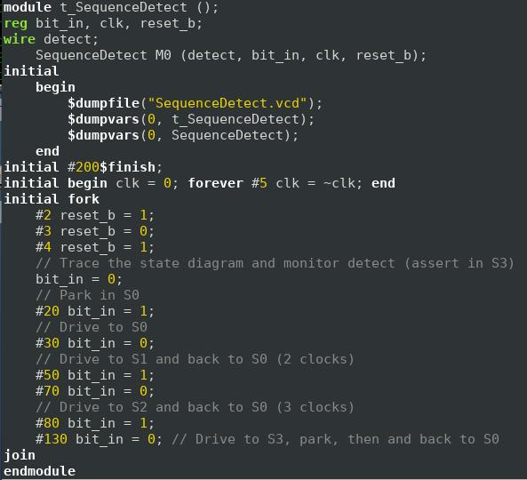
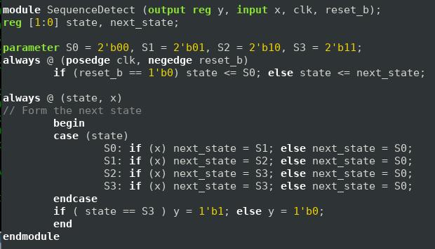
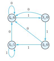
12 Suppose we wish to design a circuit that detects a sequence of three or more consecutive 1 s in a string of bits coming through an input line (i.e., the input is a serial bit stream). This is a Moore model sequential circuit, since the output is 1 when the circuit is in state S3 and is 0 otherwise. CS1026 II 12

13 The advantage of designing with D flip-flops is that the Boolean equations describing the inputs to the flip-flops can be obtained directly from the state table. We choose two D flip-flops to represent the four states, and we label their outputs A and B CS1026 II 13

14 Logic diagram of a Moore-type sequence detector CS1026 II 14

15 CS1026 II 15

16 CS1026 II 16
Chapter 5: Synchronous Sequential Logic
 Chapter 5: Synchronous Sequential Logic NCNU_2016_DD_5_1 Digital systems may contain memory for storing information. Combinational circuits contains no memory elements the outputs depends only on the inputs
Lecture 11: Synchronous Sequential Logic
 Lecture 11: Synchronous Sequential Logic Syed M. Mahmud, Ph.D ECE Department Wayne State University Aby K George, ECE Department, Wayne State University Contents Characteristic equations Analysis of clocked
Digital Design, Kyung Hee Univ. Chapter 5. Synchronous Sequential Logic
 Chapter 5. Synchronous Sequential Logic 1 5.1 Introduction Electronic products: ability to send, receive, store, retrieve, and process information in binary format Dependence on past values of inputs Sequential
1. Convert the decimal number to binary, octal, and hexadecimal.
 1. Convert the decimal number 435.64 to binary, octal, and hexadecimal. 2. Part A. Convert the circuit below into NAND gates. Insert or remove inverters as necessary. Part B. What is the propagation delay
WEEK 10. Sequential Circuits: Analysis and Design. Page 1
 WEEK 10 Sequential Circuits: Analysis and Design Page 1 Analysis of Clocked (Synchronous) Sequential Circuits Now that we have flip-flops and the concept of memory in our circuit, we might want to determine
EECS150 - Digital Design Lecture 19 - Finite State Machines Revisited
 EECS150 - Digital Design Lecture 19 - Finite State Machines Revisited April 2, 2013 John Wawrzynek Spring 2013 EECS150 - Lec19-fsm Page 1 Finite State Machines (FSMs) FSM circuits are a type of sequential
Digital Logic Design I
 Digital Logic Design I Synchronous Sequential Logic Mustafa Kemal Uyguroğlu Sequential Circuits Asynchronous Inputs Combinational Circuit Memory Elements Outputs Synchronous Inputs Combinational Circuit
Chapter 3. Boolean Algebra and Digital Logic
 Chapter 3 Boolean Algebra and Digital Logic Chapter 3 Objectives Understand the relationship between Boolean logic and digital computer circuits. Learn how to design simple logic circuits. Understand how
Switching Circuits & Logic Design, Fall Final Examination (1/13/2012, 3:30pm~5:20pm)
") Switching Circuits & Logic Design, Fall 2011 Final Examination (1/13/2012, 3:30pm~5:20pm) Problem 1: (15 points) Consider a new FF with three inputs, S, R, and T. No more than one of these inputs can be
Switching Circuits & Logic Design, Fall 2011 Final Examination (1/13/2012, 3:30pm~5:20pm) Problem 1: (15 points) Consider a new FF with three inputs, S, R, and T. No more than one of these inputs can be
Chapter 5 Synchronous Sequential Logic
 Chapter 5 Synchronous Sequential Logic Chih-Tsun Huang ( 黃稚存 ) http://nthucad.cs.nthu.edu.tw/~cthuang/ Department of Computer Science National Tsing Hua University Outline Introduction Storage Elements:
Contents Circuits... 1
 Contents Circuits... 1 Categories of Circuits... 1 Description of the operations of circuits... 2 Classification of Combinational Logic... 2 1. Adder... 3 2. Decoder:... 3 Memory Address Decoder... 5 Encoder...
`COEN 312 DIGITAL SYSTEMS DESIGN - LECTURE NOTES Concordia University
 `OEN 32 IGITL SYSTEMS ESIGN - LETURE NOTES oncordia University hapter 5: Synchronous Sequential Logic NOTE: For more eamples and detailed description of the material in the lecture notes, please refer
ECE 301 Digital Electronics
 ECE 301 Digital Electronics Derivation of Flip-Flop Input Equations and State Assignment (Lecture #24) The slides included herein were taken from the materials accompanying Fundamentals of Logic Design,
B.Tech CSE Sem. 3 15CS202 DIGITAL SYSTEM DESIGN (Regulations 2015) UNIT -IV
 UNIT -IV") B.Tech CSE Sem. 3 5CS22 DIGITAL SYSTEM DESIGN (Regulations 25) UNIT -IV SYNCHRONOUS SEQUENTIAL CIRCUITS OUTLINE FlipFlops SR,D,JK,T Analysis of Synchronous Sequential Circuit State Reduction and Assignment
B.Tech CSE Sem. 3 5CS22 DIGITAL SYSTEM DESIGN (Regulations 25) UNIT -IV SYNCHRONOUS SEQUENTIAL CIRCUITS OUTLINE FlipFlops SR,D,JK,T Analysis of Synchronous Sequential Circuit State Reduction and Assignment
Synchronous Sequential Logic
 Synchronous Sequential Logic ( 范倫達 ), Ph. D. Department of Computer Science National Chiao Tung University Taiwan, R.O.C. Fall, 2012 ldvan@cs.nctu.edu.tw http://www.cs.nctu.edu.tw/~ldvan/ Outlines Sequential
Section 6.8 Synthesis of Sequential Logic Page 1 of 8
 Section 6.8 Synthesis of Sequential Logic Page of 8 6.8 Synthesis of Sequential Logic Steps:. Given a description (usually in words), develop the state diagram. 2. Convert the state diagram to a next-state
MC9211 Computer Organization
 MC9211 Computer Organization Unit 2 : Combinational and Sequential Circuits Lesson2 : Sequential Circuits (KSB) (MCA) (2009-12/ODD) (2009-10/1 A&B) Coverage Lesson2 Outlines the formal procedures for the
Chapter 5 Sequential Circuits
 Logic and Computer Design Fundamentals Chapter 5 Sequential Circuits Part 2 Sequential Circuit Design Charles Kime & Thomas Kaminski 28 Pearson Education, Inc. (Hyperlinks are active in View Show mode)
Chapter 5 Synchronous Sequential Logic
 EEA051 - Digital Logic 數位邏輯 Chapter 5 Synchronous Sequential Logic 吳俊興國立高雄大學資訊工程學系 December 2005 Chapter 5 Synchronous Sequential Logic 5-1 Sequential Circuits 5-2 Latches 5-3 Flip-Flops 5-4 Analysis of
CHAPTER1: Digital Logic Circuits
 CS224: Computer Organization S.KHABET CHAPTER1: Digital Logic Circuits 1 Sequential Circuits Introduction Composed of a combinational circuit to which the memory elements are connected to form a feedback
Synchronous Sequential Logic
 Synchronous Sequential Logic ( 范倫達 ), Ph. D. Department of Computer Science National Chiao Tung University Taiwan, R.O.C. Fall, 2017 ldvan@cs.nctu.edu.tw http://www.cs.nctu.edu.tw/~ldvan/ Outlines Sequential
Sequential Circuits. Output depends only and immediately on the inputs Have no memory (dependence on past values of the inputs)
") Sequential Circuits Combinational circuits Output depends only and immediately on the inputs Have no memory (dependence on past values of the inputs) Sequential circuits Combination circuits with memory
Sequential Circuits Combinational circuits Output depends only and immediately on the inputs Have no memory (dependence on past values of the inputs) Sequential circuits Combination circuits with memory
UNIT III. Combinational Circuit- Block Diagram. Sequential Circuit- Block Diagram
 UNIT III INTRODUCTION In combinational logic circuits, the outputs at any instant of time depend only on the input signals present at that time. For a change in input, the output occurs immediately. Combinational
Sequential Logic. Analysis and Synthesis. Joseph Cavahagh Santa Clara University. r & Francis. TaylonSi Francis Group. , Boca.Raton London New York \
 Sequential Logic Analysis and Synthesis Joseph Cavahagh Santa Clara University r & Francis TaylonSi Francis Group, Boca.Raton London New York \ CRC is an imprint of the Taylor & Francis Group, an informa
Bachelor Level/ First Year/ Second Semester/ Science Full Marks: 60 Computer Science and Information Technology (CSc. 151) Pass Marks: 24
 Pass Marks: 24") 2065 Computer Science and Information Technology (CSc. 151) Pass Marks: 24 Time: 3 hours. Candidates are required to give their answers in their own words as for as practicable. Attempt any TWO questions:
2065 Computer Science and Information Technology (CSc. 151) Pass Marks: 24 Time: 3 hours. Candidates are required to give their answers in their own words as for as practicable. Attempt any TWO questions:
Dr.Mohamed Elmahdy Winter 2015 Eng.Yasmin Mohamed. Problem Set 6. Analysis and Design of Clocked Sequential Circuits. Discussion: 7/11/ /11/2015
 Dr. Elmahdy Winter 2015 Problem Set 6 Analysis and Design of Clocked Sequential Circuits Discussion: 7/11/2015 17/11/2015 *Exercise 6-1: (Problem 5.10) A sequential circuit has two JK flip-flops A and
The basic logic gates are the inverter (or NOT gate), the AND gate, the OR gate and the exclusive-or gate (XOR). If you put an inverter in front of
, the AND gate, the OR gate and the exclusive-or gate (XOR). If you put an inverter in front of") 1 The basic logic gates are the inverter (or NOT gate), the AND gate, the OR gate and the exclusive-or gate (XOR). If you put an inverter in front of the AND gate, you get the NAND gate etc. 2 One of the
1 The basic logic gates are the inverter (or NOT gate), the AND gate, the OR gate and the exclusive-or gate (XOR). If you put an inverter in front of the AND gate, you get the NAND gate etc. 2 One of the
ELCT201: DIGITAL LOGIC DESIGN
 ELCT201: DIGITAL LOGIC DESIGN Dr. Eng. Haitham Omran, haitham.omran@guc.edu.eg Dr. Eng. Wassim Alexan, wassim.joseph@guc.edu.eg Lecture 8 Following the slides of Dr. Ahmed H. Madian محرم 1439 ه Winter
More design examples, state assignment and reduction. Page 1
 More design examples, state assignment and reduction Page 1 Serial Parity Checker We have only 2 states (S 0, S 1 ): correspond to an even and odd number of 1 s received so far. x Clock D FF Q Z = 1 whenever
Sequential Logic Notes
 Sequential Logic Notes Andrew H. Fagg igital logic circuits composed of components such as AN, OR and NOT gates and that do not contain loops are what we refer to as stateless. In other words, the output
 UNIT 1 NUMBER SYSTEMS AND DIGITAL LOGIC FAMILIES 1. Briefly explain the stream lined method of converting binary to decimal number with example. 2. Give the Gray code for the binary number (111) 2. 3.
Combinational / Sequential Logic
 Digital Circuit Design and Language Combinational / Sequential Logic Chang, Ik Joon Kyunghee University Combinational Logic + The outputs are determined by the present inputs + Consist of input/output
The word digital implies information in computers is represented by variables that take a limited number of discrete values.
 Class Overview Cover hardware operation of digital computers. First, consider the various digital components used in the organization and design. Second, go through the necessary steps to design a basic
Part II. Chapter2: Synchronous Sequential Logic
 課程名稱 : 數位系統設計導論 P-/77 Part II Chapter2: Synchronous Sequential Logic 教師 : 郭峻因教授 INSTRUCTOR: Prof. Jiun-In Guo E-mail: jiguo@cs.ccu.edu.tw 課程名稱 : 數位系統設計導論 P-2/77 Special thanks to Prof. CHING-LING SU for
CSE Latches and Flip-flops Dr. Izadi. NOR gate property: A B Z Cross coupled NOR gates: S M S R Q M
 CSE-4523 Latches and Flip-flops Dr. Izadi NOR gate property: A B Z A B Z Cross coupled NOR gates: S M S R M R S M R S R S R M S S M R R S ' Gate R Gate S R S G R S R (t+) S G R Flip_flops:. S-R flip-flop
Solution to Digital Logic )What is the magnitude comparator? Design a logic circuit for 4 bit magnitude comparator and explain it,
What is the magnitude comparator? Design a logic circuit for 4 bit magnitude comparator and explain it,") Solution to Digital Logic -2067 Solution to digital logic 2067 1.)What is the magnitude comparator? Design a logic circuit for 4 bit magnitude comparator and explain it, A Magnitude comparator is a combinational
Solution to Digital Logic -2067 Solution to digital logic 2067 1.)What is the magnitude comparator? Design a logic circuit for 4 bit magnitude comparator and explain it, A Magnitude comparator is a combinational
cs281: Introduction to Computer Systems Lab07 - Sequential Circuits II: Ant Brain
 cs281: Introduction to Computer Systems Lab07 - Sequential Circuits II: Ant Brain 1 Problem Statement Obtain the file ant.tar from the class webpage. After you untar this file in an empty directory, you
ELE2120 Digital Circuits and Systems. Tutorial Note 8
 ELE2120 Digital Circuits and Systems Tutorial Note 8 Outline 1. Register 2. Counters 3. Synchronous Counter 4. Asynchronous Counter 5. Sequential Circuit Design Overview 1. Register Applications: temporally
CS302 - Digital Logic Design FAQs By
 CS302 - Digital Logic Design FAQs By For BCD numbers that add up to an invalid BCD number or generate a carry the number 6 (0110) is added to the invalid number, why? These binary numbers are not allowed
Universidad Carlos III de Madrid Digital Electronics Exercises
 1. Complete the chronogram for the circuit given in the figure. inst7 NOT A INPUT VCC AND2 inst5 DFF D PRN Q CLRN inst XOR inst2 TFF PRN T Q CLRN inst8 OUTPUT OUTPUT Q Q1 CLK INPUT VCC CLEARN INPUT VCC
Encoders and Decoders: Details and Design Issues
 Encoders and Decoders: Details and Design Issues Edward L. Bosworth, Ph.D. TSYS School of Computer Science Columbus State University Columbus, GA 31907 bosworth_edward@colstate.edu Slide 1 of 25 slides
EE292: Fundamentals of ECE
 EE292: Fundamentals of ECE Fall 2012 TTh 10:00-11:15 SEB 1242 Lecture 23 121120 http://www.ee.unlv.edu/~b1morris/ee292/ 2 Outline Review Combinatorial Logic Sequential Logic 3 Combinatorial Logic Circuits
Sequential Logic Circuits
 Sequential Logic Circuits By Dr. M. Hebaishy Digital Logic Design Ch- Rem.!) Types of Logic Circuits Combinational Logic Memoryless Outputs determined by current values of inputs Sequential Logic Has memory
Chapter 11 State Machine Design
 Chapter State Machine Design CHAPTER OBJECTIVES Upon successful completion of this chapter, you will be able to: Describe the components of a state machine. Distinguish between Moore and Mealy implementations
NH 67, Karur Trichy Highways, Puliyur C.F, Karur District UNIT-III SEQUENTIAL CIRCUITS
 NH 67, Karur Trichy Highways, Puliyur C.F, 639 114 Karur District DEPARTMENT OF ELETRONICS AND COMMUNICATION ENGINEERING COURSE NOTES SUBJECT: DIGITAL ELECTRONICS CLASS: II YEAR ECE SUBJECT CODE: EC2203
CHAPTER 4: Logic Circuits
 CHAPTER 4: Logic Circuits II. Sequential Circuits Combinational circuits o The outputs depend only on the current input values o It uses only logic gates, decoders, multiplexers, ALUs Sequential circuits
UNIT 1: DIGITAL LOGICAL CIRCUITS What is Digital Computer? OR Explain the block diagram of digital computers.
 UNIT 1: DIGITAL LOGICAL CIRCUITS What is Digital Computer? OR Explain the block diagram of digital computers. Digital computer is a digital system that performs various computational tasks. The word DIGITAL
CPS311 Lecture: Sequential Circuits
 CPS311 Lecture: Sequential Circuits Last revised August 4, 2015 Objectives: 1. To introduce asynchronous and synchronous flip-flops (latches and pulsetriggered, plus asynchronous preset/clear) 2. To introduce
Chapter 5 Sequential Circuits
 Logic and omputer Design Fundamentals hapter 5 Sequential ircuits Part 1 Storage Elements and Sequential ircuit Analysis harles Kime & Thomas Kaminski 2008 Pearson Education, Inc. (Hyperlinks are active
 WWW.STUDENTSFOCUS.COM + Class Subject Code Subject Prepared By Lesson Plan for Time: Lesson. No 1.CONTENT LIST: Introduction to Unit III 2. SKILLS ADDRESSED: Listening I year, 02 sem CS6201 Digital Principles
To design a sequential logic circuit using D-Flip-flop. To implement the designed circuit.
 6.1 Objectives To design a sequential logic circuit using D-Flip-flop. To implement the designed circuit. 6.2 Sequential Logic So far we have implemented digital circuits whose outputs depend only on its
Course Administration
 EE 224: INTRODUCTION TO DIGITAL CIRCUITS & COMPUTER DESIGN Lecture 5: Sequential Logic - 2 Analysis of Clocked Sequential Systems 4/2/2 Avinash Kodi, kodi@ohio.edu Course Administration 2 Hw 2 due on today
Midterm Examination II
 Midterm Examination II EE 203 - Digital Systems DESIGN (Fall 2015) MEF University Instructions Assigned: 6:30pm on December 17, 2015. Due: 8:00pm on December 17, 2015. Instructor: Şuayb Ş. Arslan. Name:
2 Sequential Circuits
 2 2.1 State Diagrams and General Form 0/0 1/0 Start State 0 /0 1/1 State 1 /1 0/1 State Diagram of a Change Detector ( Mealy-machine). The output Y assumes 1 whenever the input X has changed. Otherwise
DIGITAL SYSTEM DESIGN UNIT I (2 MARKS)
") DIGITAL SYSTEM DESIGN UNIT I (2 MARKS) 1. Convert Binary number (111101100) 2 to Octal equivalent. 2. Convert Binary (1101100010011011) 2 to Hexadecimal equivalent. 3. Simplify the following Boolean function
DIGITAL SYSTEM DESIGN UNIT I (2 MARKS) 1. Convert Binary number (111101100) 2 to Octal equivalent. 2. Convert Binary (1101100010011011) 2 to Hexadecimal equivalent. 3. Simplify the following Boolean function
Synchronous sequential circuits
 8.6.5 Synchronous sequential Table of content. Combinational circuit design. Elementary combinatorial for data transmission. Memory structures 4. Programmable logic devices 5. Algorithmic minimization
UNIT IV. Sequential circuit
 UNIT IV Sequential circuit Introduction In the previous session, we said that the output of a combinational circuit depends solely upon the input. The implication is that combinational circuits have no
Department of CSIT. Class: B.SC Semester: II Year: 2013 Paper Title: Introduction to logics of Computer Max Marks: 30
 Department of CSIT Class: B.SC Semester: II Year: 2013 Paper Title: Introduction to logics of Computer Max Marks: 30 Section A: (All 10 questions compulsory) 10X1=10 Very Short Answer Questions: Write
In this lecture we will work through a design example from problem statement to digital circuits.
 Lecture : A Design Example - Traffic Lights In this lecture we will work through a design example from problem statement to digital circuits. The Problem: The traffic department is trying out a new system
EECS150 - Digital Design Lecture 15 Finite State Machines. Announcements
 EECS150 - Digital Design Lecture 15 Finite State Machines October 18, 2011 Elad Alon Electrical Engineering and Computer Sciences University of California, Berkeley http://www-inst.eecs.berkeley.edu/~cs150
Chapter 5. Introduction
 Chapter 5 Synchronous Sequential Logic Chapter 5 Introduction Circuits require memory to store intermediate data Sequential circuits use a periodic signal to determine when to store values. A clock signal
Logic Design II (17.342) Spring Lecture Outline
 Spring Lecture Outline") Logic Design II (17.342) Spring 2012 Lecture Outline Class # 05 February 23, 2012 Dohn Bowden 1 Today s Lecture Analysis of Clocked Sequential Circuits Chapter 13 2 Course Admin 3 Administrative Admin
Logic Design II (17.342) Spring 2012 Lecture Outline Class # 05 February 23, 2012 Dohn Bowden 1 Today s Lecture Analysis of Clocked Sequential Circuits Chapter 13 2 Course Admin 3 Administrative Admin
AM AM AM AM PM PM PM
 FACULTY OF ENGINEERING AND TECHNOLOGY DEPARTMENT OF COMPUTER SCIENCE & ENGINEERING COURSE PLAN Course Code : CS0003 Course Title : DIGITAL COMPUTER FUNDAMENTALS Semester : III Course Time : Jun 204 to
Synchronous Sequential Logic. Chapter 5
 Synchronous Sequential Logic Chapter 5 5-1 Introduction Combinational circuits contains no memory elements the outputs depends on the inputs Synchronous Sequential Logic 5-2 5-2 Sequential Circuits Sequential
COMP2611: Computer Organization. Introduction to Digital Logic
 1 COMP2611: Computer Organization Sequential Logic Time 2 Till now, we have essentially ignored the issue of time. We assume digital circuits: Perform their computations instantaneously Stateless: once
Find the equivalent decimal value for the given value Other number system to decimal ( Sample)
") VELAMMAL COLLEGE OF ENGINEERING AND TECHNOLOGY, MADURAI 65 009 Department of Information Technology Model Exam-II-Question bank PART A (Answer for all Questions) (8 X = 6) K CO Marks Find the equivalent
VELAMMAL COLLEGE OF ENGINEERING AND TECHNOLOGY, MADURAI 65 009 Department of Information Technology Model Exam-II-Question bank PART A (Answer for all Questions) (8 X = 6) K CO Marks Find the equivalent
CHAPTER 4: Logic Circuits
 CHAPTER 4: Logic Circuits II. Sequential Circuits Combinational circuits o The outputs depend only on the current input values o It uses only logic gates, decoders, multiplexers, ALUs Sequential circuits
Digital Principles and Design
 Digital Principles and Design Donald D. Givone University at Buffalo The State University of New York Grauu Boston Burr Ridge, IL Dubuque, IA Madison, Wl New York San Francisco St. Louis Bangkok Bogota
Department of Computer Science and Engineering Question Bank- Even Semester:
 Department of Computer Science and Engineering Question Bank- Even Semester: 2014-2015 CS6201& DIGITAL PRINCIPLES AND SYSTEM DESIGN (Common to IT & CSE, Regulation 2013) UNIT-I 1. Convert the following
Logic Design II (17.342) Spring Lecture Outline
 Spring Lecture Outline") Logic Design II (17.342) Spring 2012 Lecture Outline Class # 03 February 09, 2012 Dohn Bowden 1 Today s Lecture Registers and Counters Chapter 12 2 Course Admin 3 Administrative Admin for tonight Syllabus
Logic Design II (17.342) Spring 2012 Lecture Outline Class # 03 February 09, 2012 Dohn Bowden 1 Today s Lecture Registers and Counters Chapter 12 2 Course Admin 3 Administrative Admin for tonight Syllabus
Computer Architecture and Organization
 A-1 Appendix A - Digital Logic Computer Architecture and Organization Miles Murdocca and Vincent Heuring Appendix A Digital Logic A-2 Appendix A - Digital Logic Chapter Contents A.1 Introduction A.2 Combinational
Logic and Computer Design Fundamentals. Chapter 7. Registers and Counters
 Logic and Computer Design Fundamentals Chapter 7 Registers and Counters Registers Register a collection of binary storage elements In theory, a register is sequential logic which can be defined by a state
EXPERIMENT 13 ITERATIVE CIRCUITS
 EE 2449 Experiment 13 Revised 4/17/2017 CALIFORNIA STATE UNIVERSITY LOS ANGELES Department of Electrical and Computer Engineering EE-246 Digital Logic Lab EXPERIMENT 13 ITERATIVE CIRCUITS Text: Mano, Digital
CPSC 121: Models of Computation. Module 1: Propositional Logic
 CPSC 121: Models of Computation Module 1: Propositional Logic Module 1: Propositional Logic By the start of the class, you should be able to: Translate back and forth between simple natural language statements
1. a) For the circuit shown in figure 1.1, draw a truth table showing the output Q for all combinations of inputs A, B and C. [4] Figure 1.
![1. a) For the circuit shown in figure 1.1, draw a truth table showing the output Q for all combinations of inputs A, B and C. [4] Figure 1.](/thumbs/88/117492374.jpg "1. a) For the circuit shown in figure 1.1, draw a truth table showing the output Q for all combinations of inputs A, B and C. [4] Figure 1.") [Question 1 is compulsory] 1. a) For the circuit shown in figure 1.1, draw a truth table showing the output Q for all combinations of inputs A, B and C. Figure 1.1 b) Minimize the following Boolean functions:
[Question 1 is compulsory] 1. a) For the circuit shown in figure 1.1, draw a truth table showing the output Q for all combinations of inputs A, B and C. Figure 1.1 b) Minimize the following Boolean functions:
Previous Lecture Sequential Circuits. Slide Summary of contents covered in this lecture. (Refer Slide Time: 01:55)
") Previous Lecture Sequential Circuits Digital VLSI System Design Prof. S. Srinivasan Department of Electrical Engineering Indian Institute of Technology, Madras Lecture No 7 Sequential Circuit Design Slide
Previous Lecture Sequential Circuits Digital VLSI System Design Prof. S. Srinivasan Department of Electrical Engineering Indian Institute of Technology, Madras Lecture No 7 Sequential Circuit Design Slide
BISHOP ANSTEY HIGH SCHOOL & TRINITY COLLEGE EAST SIXTH FORM CXC CAPE PHYSICS, UNIT 2 Ms. S. S. CALBIO NOTES lesson #39
 BISHOP ANSTEY HIGH SCHOOL & TRINITY COLLEGE EAST SIXTH FORM CXC CAPE PHYSICS, UNIT 2 Ms. S. S. CALBIO NOTES lesson #39 Objectives: Students should be able to Thursday 21 st January 2016 @ 10:45 am Module
Logic Devices for Interfacing, The 8085 MPU Lecture 4
 Logic Devices for Interfacing, The 8085 MPU Lecture 4 1 Logic Devices for Interfacing Tri-State devices Buffer Bidirectional Buffer Decoder Encoder D Flip Flop :Latch and Clocked 2 Tri-state Logic Outputs
Quiz #4 Thursday, April 25, 2002, 5:30-6:45 PM
 Last (family) name: First (given) name: Student I.D. #: Circle section: Hu Saluja Department of Electrical and Computer Engineering University of Wisconsin - Madison ECE/CS 352 Digital System Fundamentals
Figure 30.1a Timing diagram of the divide by 60 minutes/seconds counter
 Digital Clock The timing diagram figure 30.1a shows the time interval t 6 to t 11 and t 19 to t 21. At time interval t 9 the units counter counts to 1001 (9) which is the terminal count of the 74x160 decade
Final Exam review: chapter 4 and 5. Supplement 3 and 4
 Final Exam review: chapter 4 and 5. Supplement 3 and 4 1. A new type of synchronous flip-flop has the following characteristic table. Find the corresponding excitation table with don t cares used as much
11.1 As mentioned in Experiment 10, sequential logic circuits are a type of logic circuit where the output
 EE 2449 Experiment JL and NWP //8 CALIFORNIA STATE UNIVERSITY LOS ANGELES Department of Electrical and Computer Engineering EE-2449 Digital Logic Lab EXPERIMENT SEQUENTIAL CIRCUITS Text: Mano and Ciletti,
ECE 25 Introduction to Digital Design. Chapter 5 Sequential Circuits ( ) Part 1 Storage Elements and Sequential Circuit Analysis
 Part 1 Storage Elements and Sequential Circuit Analysis") EE 25 Introduction to igital esign hapter 5 Sequential ircuits (5.1-5.4) Part 1 Storage Elements and Sequential ircuit Analysis Logic and omputer esign Fundamentals harles Kime & Thomas Kaminski 2008 Pearson
EE 25 Introduction to igital esign hapter 5 Sequential ircuits (5.1-5.4) Part 1 Storage Elements and Sequential ircuit Analysis Logic and omputer esign Fundamentals harles Kime & Thomas Kaminski 2008 Pearson
Subject : EE6301 DIGITAL LOGIC CIRCUITS
 QUESTION BANK Programme : BE Subject : Semester / Branch : III/EEE UNIT 1 NUMBER SYSTEMS AND DIGITAL LOGIC FAMILIES Review of number systems, binary codes, error detection and correction codes (Parity
Sequential Logic and Clocked Circuits
 Sequential Logic and Clocked Circuits Clock or Timing Device Input Variables State or Memory Element Combinational Logic Elements From combinational logic, we move on to sequential logic. Sequential logic
EXPERIMENT: 1. Graphic Symbol: OR: The output of OR gate is true when one of the inputs A and B or both the inputs are true.
 EXPERIMENT: 1 DATE: VERIFICATION OF BASIC LOGIC GATES AIM: To verify the truth tables of Basic Logic Gates NOT, OR, AND, NAND, NOR, Ex-OR and Ex-NOR. APPARATUS: mention the required IC numbers, Connecting
AC103/AT103 ANALOG & DIGITAL ELECTRONICS JUN 2015
 Q.2 a. Draw and explain the V-I characteristics (forward and reverse biasing) of a pn junction. (8) Please refer Page No 14-17 I.J.Nagrath Electronic Devices and Circuits 5th Edition. b. Draw and explain
Modeling Digital Systems with Verilog
 Modeling Digital Systems with Verilog Prof. Chien-Nan Liu TEL: 03-4227151 ext:34534 Email: jimmy@ee.ncu.edu.tw 6-1 Composition of Digital Systems Most digital systems can be partitioned into two types
problem maximum score 1 28pts 2 10pts 3 10pts 4 15pts 5 14pts 6 12pts 7 11pts total 100pts
 University of California at Berkeley College of Engineering Department of Electrical Engineering and Computer Sciences EECS150 J. Wawrzynek Spring 2002 4/5/02 Midterm Exam II Name: Solutions ID number:
Introduction to Digital Electronics
 Introduction to Digital Electronics by Agner Fog, 2018-10-15. Contents 1. Number systems... 3 1.1. Decimal, binary, and hexadecimal numbers... 3 1.2. Conversion from another number system to decimal...
Registers and Counters
 Registers and Counters Clocked sequential circuit = F/Fs and combinational gates Register Group of flip-flops (share a common clock and capable of storing one bit of information) Consist of a group of
LATCHES & FLIP-FLOP. Chapter 7
 LATCHES & FLIP-FLOP Chapter 7 INTRODUCTION Latch and flip flops are categorized as bistable devices which have two stable states,called SET and RESET. They can retain either of this states indefinitely
DIGITAL TECHNICS II. Dr. Bálint Pődör. Óbuda University, Microelectronics and Technology Institute
 26.3.9. DIGITAL TECHNICS II Dr. Bálint Pődör Óbuda University, Microelectronics and Technology Institute 5. LECTURE: ANALYSIS AND SYNTHESIS OF SYNCHRONOUS SEQUENTIAL CIRCUITS 2nd (Spring) term 25/26 5.
ELEN Electronique numérique
 ELEN0040 - Electronique numérique Patricia ROUSSEAUX Année académique 2014-2015 CHAPITRE 5 Sequential circuits design - Timing issues ELEN0040 5-228 1 Sequential circuits design 1.1 General procedure 1.2
ECE 331 Digital System Design
 ECE 331 Digital System Design Counters (Lecture #20) The slides included herein were taken from the materials accompanying Fundamentals of Logic Design, 6 th Edition, by Roth and Kinney, and were used
ECE 301 Digital Electronics
 ECE 301 Digital Electronics Counters (Lecture #20) The slides included herein were taken from the materials accompanying Fundamentals of Logic Design, 6 th Edition, by Roth and Kinney, and were used with
Fall 2000 Chapter 5 Part 1
 ECE/CS 352 Digital Systems Fundamentals Fall 2000 Chapter 5 Part 1 Tom Kaminski & Charles R. Kime ECE/CS 352 Digital System Fundamentals T. Kaminski & C. Kime 1 Registers A register is a collection of
L5 Sequential Circuit Design
 L Sequential Circuit Design Sequential Circuit Design Mealy and Moore Characteristic Equations Design Procedure Example Sequential Problem from specification to implementation Ref: Unit 14 of text 9/2/2012
Counters. ENT 263 Digital Electronics
 Counters ENT 263 Digital Electronics Objectives Describe the difference between an asynchronous and a synchronous counter Analyze counter timing diagram Analyze counter circuits Determine the sequence
Registers and Counters
 Registers and Counters ( 范倫達 ), Ph. D. Department of Computer Science National Chiao Tung University Taiwan, R.O.C. Fall, 2011 ldvan@cs.nctu.edu.tw http://www.cs.nctu.edu.tw/~ldvan/ Registers Shift Registers