Advanced Pattern Generator Technology
|
|
|
- Kelly Alexander
- 6 years ago
- Views:
Transcription


1 Advanced Pattern Generator Technology Unlock the full nanopatterning potential of your SEM, FIB-SEM, or HIM Nanolithography and nanofabrication for all focused electron and ion beam microscopes NANOLITHOGRAPHY AND NANOFABRICATION UPGRADE KITS

 Automated complex")

 Proximity")
2 ELPHY Create your own nanolithography system and get free access to Raith s worldwide support infrastructure ELPHY sets the benchmark: Professional semiconductor industry standard GDSII file handling Flexible directional scanning mode / nanopatterning strategies ( FLEXposure ) Automated complex pattern sequencing using task list (e.g. involving macros, scripts, multiple beams, drift correction ) Proximity effect correction and true 3D nanofabrication Unique multiplying DAC concept for multilevel lithography, calibration and sub-nm pitch control A. Rey, IBM Research Zurich & ETHZ Nanotechnology group, Switzerland

 or Focused Ion Beam (FIB) patterning,")
 are must")


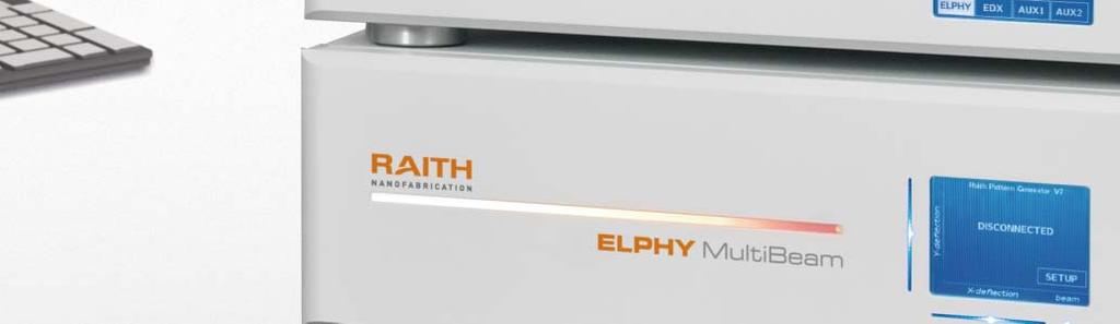
3 ELPHY The key to nanofabrication Accelerate your SEM / FIB-SEM / HIM In today s research laboratories, Electron Beam Lithography (EBL) or Focused Ion Beam (FIB) patterning, milling, Focused Electron or Ion Beam Induced Processes (FEBIP/ FIBIP) are must have technologies. For more than 25 years, Raith has been pioneering the most economic conversion of virtually any SEM or FIB into nanolithography / nanofabrication stations in order to fully exploit their nanopatterning potential. ELPHY attachments significantly enlarge the bandwidth, complexity, and degree of automation of possible nanofabrication applications when adapted to these tools. More than 100 person-years of software development, paired with mature and advanced pattern generator technology, make ELPHY the most comprehensive and successful nanolithography / nanofabrication upgrade kit in the world given a track record of about 1,000 installations! Flexibility / Ease of use Complexity / Automation Purpose-built hardware Whether adapted to an SEM, a FIB, a FIB-SEM or a HIM, ELPHY is capable of handling a whole range of tasks, from simple single write field tasks to complex and highly automated multi-level and multi-field patterning processes or metrology jobs. Raith s decades of expertise in the field of nanofabrication with both electrons and ions is embodied in the most comprehensive Raith software. The entire nano fabrication workflow, spanning pro fessional GDSII design, post-processing, alignment, exposure / patterning parameter control, automation, and microscope remote control, is fully integrated into a single intuitive user interface. In all Raith nanofabrication products whether using ELPHY or a Raith turnkey system you will find the same synergetic software platform: the Raith Nanosuite. This ensures that the entire workflow and most advanced nanofabrication function ality is already implemented in ELPHY. For example, every ELPHY system provides proximity effect correction or true 3D nanofabrication algorithms, flexible directional scanning mode / nanopatterning strategies ( FLEX posure ), multilevel lithography with multiple automatic alignment, overlay and mark recognition features, automatic drift correction combinable with a comprehensive macro library, script control or process evaluation / metrology functionality. Best electronic signal quality resulting in most accurate pattern placement at highest writing speed are the main development targets of every Raith pattern processor. All Raith pattern generators use a dedicated hardware concept for multilevel lithography / nanofabrication, calibration, and grating pitch control. Like genuine e-beam writers, Raith s ELPHY system also offers 6 multiplying 16-bit D / A converters in addition to the 16-bit main-deflection D / A converters, yielding a non-compromise writefield alignment, highest overlay precision, and a superior patterning resolution in the sub-nm regime (equivalent to far more than 16-bit). ELPHY MultiBeam ELPHY Plus ELPHY Quantum 3


, Electron Beam")
 and Helium Ion Beam Patterning.")
 in highest quality using concentric elliptical")


4 ELPHY MultiBeam The nanopatterning benchmark One pattern generator for both electron and ion beam control ELPHY MultiBeam sets new standards in the market for SEM, FIB-SEM and HIM nanolithography solutions ( attachments ). ELPHY MultiBeam combines the latest technology for three-dimensional IBL and other 3D nanofabrication techniques with the very best EBL performance, and helps to unlock the full nanofabrication potential of your SEM, FIB-SEM or HIM system. Highest accuracy nanopatterning by advanced process control Applications with demanding dimensionality and stability requirements need ultimate flexibility with respect to nanopatterning strategy. Raith s FLEXposure software modules, using specific directional patterning modes and other patterning attributes such as loops, help you to significantly optimize the definition of your nanostructure. Drift correction functionality ensures highly accurate pattern placement, especially during long term exposures or milling jobs. ELPHY MultiBeam includes all comprehensive multiple technique nanopatterning functionality in a single system, relevant for advanced Focused Ion Beam Milling, Etching and Deposition, Ion Beam Litho g raphy (IBL), Electron Beam Lithography (EBL), Gas Assisted Focused Electron Beam Induced Processing (FEBIP) and Helium Ion Beam Patterning. Photonic crystal fabricated in a direct milling process with a FIB-SEM (a) in conventional way and (b) in highest quality using concentric elliptical patterning mode (outwards), drift correction schemes, and GDSII element loops as patterning attributes. 1 μm FIB Nanopatterning with fully automated closed loop size control SEM FIB: Size corrected milling 100% of target depth FIB FIB: Initial milling 20% of target depth Automated rescaling evaluation Line scan SEM: Line scan analysis 2 Automatic stage tilt Line scan Dynamic milling process verification by closed loop dimensional SEM feedback in a fully automated sequential process involving both electron and ion column. The task was to mill a perfect square with edge length exactly 5 μm on the spot without time-consuming iterative cycles. Linescan metrology was used to automatically compensate for scaling errors during the milling process at 20% target milling depth and a 0.2% dimensional accuracy was achieved. 4


5 ELPHY MultiBeam The nanopatterning benchmark Unique features for convenient operation Patterning-on-image ( directaligndesign ) functionality enables new nano structures to be inserted into existing features on your sample with out the need for alignment routines. After taking an image, a GDSII design can immediately be drawn on top before launching a nanopatterning job with perfect overlay and without additional alignment procedures. Standard nanopatterning such as electron beam lithography nano patterning followed by a complementary FIB process step has been used to create a convenient Hall bar device manufacturing process (see image to the right). The recipe manager helps to shorten long design / parameter setup cycles; just drag and drop a recipe onto your existing GDSII design elements, thus assigning a specific parameter set from a freely definable database. The Signal Router minimizes the number of one (or more sequentially con- EBL EBL FIB EBL Combined EBL / FIB nanofabrication process of a (Nano) Hall bar ( nm). First Cd 3 As 2 nano plates and contacts were fabricated using EBL and metal deposition; in a second step FIB was used to etch the samples into Hall bar geometry; W. Wang et al., Fudan University, Shanghai, China nected) switchboxes. 4 input and 3 output channels smoothly integrate further accessories such as EDX to be connect ed to the same or several external scan interfaces. The Signal EBL EBL EBL Router can also be used for fully automated processes, e.g. involving both FIB milling and SEM metrology, for automated dynamic FIB milling process verification. A benchmark pattern generator for high-performing sensitive instruments ELPHY MultiBeam has been designed to match the needs of ultimate pattern ing performance with highest placement accuracy and resolution. Differential signal outputs ensure maximum signal to noise ratio in conjunction with high-performing sensitive instruments such as helium ion microscopes (HIM). 100 nm 50 nm TEM images of nanopores (milled in concentric outwards and dot patterning mode) down to sub 10 nm, 5 nm and ~2 nm diameter respectively, fabricated in thin carbon nano membranes using a helium ion microscope controlled by ELPHY MultiBeam. D. Emmrich, A.Gölzhäuser et al., Uni Bielefeld, Germany 5

 technology and Raith s unsurpassed software user interface")


6 ELPHY Plus The professional nanolithography attachment The solution for state-of-the-art SEM or FIB instruments ELPHY Plus is a truely professional lithography attachment for SEM and FIB systems. Digital signal processor (DSP) technology and Raith s unsurpassed software user interface makes this pattern generator the ideal complement for all state-of-the-art FE-SEM and FIB systems. More results per day Combining ultra-high resolution nanostructures and large area exposures in a single run (e.g. for contacting nanostructures to the macroscopic world) is a very common application. Both nanostructures and large area structures need to match and have to be exposed in a single, preferably automatic run including alignment routines. ELPHY s split exposure functionality can switch between smallest beam currents for highest-resolution nanostructures patterning and high beam currents for large area exposures in a fully automated exposure sequence. Applying the latter makes ELPHY Plus very efficient, particularly if attached to modern thermal field emission based SEMs with high beam current densities or excellent low kv performance. Ultimate electronic performance The ELPHY Plus pattern processor has been designed with utmost care in order to deliver unequalled elec tronic performance. ELPHY Plus is designed as a separate 19-inch electronic rack unit with meticulous RF shielding and is equipped with Peltier-cooled temperature-stabilized D / A converters. These are undeniable prerequisites for nanolithography with ultimate resolution, precision and stability, especially when it comes to long term nanopatterning jobs. 3mm m 1 μm Efficiently contacting nanostructures to the outside world by split exposure functionality: Fully automted patterning sequence involving automatic switching between specific set of exposure parameters for ultrahigh-resolution nanostructures (small beam current for high-precision pattern placement and definition) and large area contact pads (high beam current for efficient patterning). ELPHY Plus Applications 1 μm CMOS decoder circuit, aligned e-beam pattern with CMOS Metal 5 vias Kuk-Hwan Kim, EECS, University of Michigan, USA Photonic crystal structure in membrane (underetched) William Whelan-Curtin, University of St. Andrews, UK Step-and-Flash Imprint Lithography (S-FIL) imprint of a motheye lens, mold fabricated by 3D-FIBlithography J. Kettle, Cardiff University, UK 6


, integrated into a single user interface, the")


7 ELPHY Quantum The universal nanolithography attachment Optimum value for money ELPHY Quantum represents the most economical access to professional nanolithography and nanofabrication providing all you need to get started efficiently! ELPHY Quantum covers the entire workflow (CAD layout and processing, control of exposure parameters, automation, remote control of each microscope etc.), integrated into a single user interface, the Raith Nanosuite. The proprietary hardware is preinstalled and tested and operates under a high-end workstation, utilizing a most recent Windows operating system. Proprietary hardware for highprecision nanopatterning ELPHY Quantum is the most universal and flexible lithography attachment for SEM and FIB systems. ELPHY Quantum consists of advanced PCIboard-based, noise-protected and deglitched scan generator electronics. A 6-fold multiplying DAC matrix modifies the analog output signal from the primary DACs such that the maximum DAC range can still be used for patterning without loss in signal-to-noise ratio at all write field orientations and sizes. Other benefits from the concept arise when applied to specific applications in communica tion technology and integrated optics such as DFB laser gratings, which can be fine tuned to specific wavelengths with sub-nm resolution. Connecting nanostructures with the macroscopic world One of ELPHY Quantum s strengths is its simple and flexible overlay functionality, with the help of which nanostructures such as carbon nanotubes, nanowires, nanojunctions, nanodevices, or graphene flakes can be connected to large contact pads for measurement of various physical properties. Sophisticated manual or fully automatic mark recognition and alignment routines help you with these multilevel lithography applications for highest-accuracy nanostructure definition and / or its connection to the outer world. 200 nm Aharonov-Bohm ring with 1D Quantum Wire (QW) embedded in one of the ring-gate structure arms A. Tsukernik, Tel Aviv University, Israel AI nanobridge used as a tunneling contact (after mechanical break) M. Goffman, CEA Saclay, France; E. Scheer, University of Konstanz, Germany The Universal Sample Holder The universal sample holder (USH) can be purchased as an option with all ELPHY systems. It is compatible with almost any instrument in the field and comprises a calibration standard (CHESSY) and an integrated Faraday cup. Three clamps for small ~cm 2 - samples or small wafer pieces are provided. Graphene device fabrication: a) SEM image of Graphene flake b) GDSII-design overlay for mesa and contacts c) mesa and contact formation Fred Schedin, Andre Geim et al., University of Manchester, England 7


8 The Raith Nanosuite The most comprehensive nanolithography software One software platform for all Raith ELPHY products Whether you use ELPHY Quantum, ELPHY Plus or the premium ELPHY MultiBeam system, all software is based on the Raith Nanosuite, which also serves as a platform for the entire Raith product portfolio. This means, all your designs and processes will be compatible even when using a Raith turnkey system. All you need to start exposing your first patterns is included in the standard scope of delivery: Professional GDSII CAD layout editor, exposure parameter determination, task list for step and repeat exposures, automated or user assisted mark registration for multilevel lithography, mix & match application, or stage / column control drivers. If required, proximity effect correction and CAD layout postprocessing are available and seamlessly integrated into your lithography control software. If you need to generate 3-dimensional (grayscale) structures for e.g. integrated optics application, additional software is available to calculate the correct exposure dose distribution. GDSII viewer / editor A key advantage of having this fully integrated viewer and editor is to eliminate data conversion steps from external layout software. All changes of dimensions or, especially, patterning parameter doses are made directly in ELPHY s editor. Patterning processes can be started immediately without the need for further compilation. If preferred, standard formats like GDSII, DXF, CIF, ASCII can be imported from AutoCAD, DesignCAD, or other GDSII layout software. Like professional dedicated e-beam writers, ELPHY data management uses the industry standard of (hierarchical) GDSII. Raith Nanosuite with Integrated GDSII layout editor 8


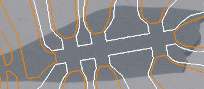
9 The Raith Nanosuite All modules integrated Patterning / Automation In order to achieve optimum patterning results, writing strategies are kept very flexible. Full control over all exposure or milling parameters is given. Automated step and repeat exposures are easily controlled by editing a position list (task list) or using dragand-drop features. They can also be embedded in a complex, fully automated patterning process sequence containing not only the mere patterning jobs, but also macros or scripts for column setup or exposure parameter changes, drift, beam current or focus correction, and automated complex metrology tasks. When finished, the system can even activate a column standby mode and deliver an immediate message to the system operator s office PC to maximize efficiency of system usage with highest job yield. FLEXposure attributing per pattern shape within GDSII, multiple choice of directional patterning in total 5 main operating modes with 47 submodes Parameter calculation functionality: Automatic correlated calculation of correct exposure parameters, also taking into account specific dose factors / parameters for curved elements, lines and dots. Positionlist: Powerful tool to define a task list containing fully automated subsequent jobs whether type patterning, alignment, parameter changes, calibration, metrology, automated calculation thereof, macro / scripting, or switching the instrument to standby mode after job completion. The system can even send the user an after job termination. Multilevel lithography Many lithography applications require alignment to existing structures / patterns. ELPHY systems offer hardware alignment, meaning the writing field orientation is physically shifted / scaled / rotated relative to the fixed sample with the help of 6 additional multiplying D / A converters. The alignment accuracy achieved is typically to the order of very few 10 nm and is much better than that obtained with virtually any motorized stage. The user can assist during the mark registration procedure or apply fully automated mark registration sequences. Example for a (subsequent design layer 1-3) mult i- level lithography process for high electron mobility transistor (HEMT) fabrication (3-layer GDSII design with alignment marks). Optimizing alignment accuracy by means of threshold / edge detection algorithms respectively. 9


 with the help of 3D resist development simulation for")
 applications are finding their way to e.g. optics or optoelectronics.")
10 The Raith Nanosuite Sets the standard Metrology Nanofabrication is one task, but efficient dimensionality check and respective subsequent process optimization quite a different one. However, they can all be accomplished using a powerful set of metrology algorithms and filters within the Raith Nanosuite, such as edge or distance detection, threshold, noise reduction, or cross correlation, to name but a few all automatable and exportable in e.g. histogram format for further analysis and evaluation. Automatic pitch detection metrology algorithm of a 200 nm grating with λ / 4 phase shift resulting in a distance of ~250 nm at phase shift position. Proximity Effect Correction and 3D resist exposure simulation Some applications require very accurate dose control in order to deliver optimum clearing doses, which can be crucial for fabrication of dense nanostructures such as optical gratings or photonic crystals. The proximity effect correction package NanoPECS helps to optimize dose distribution for critical parts of your design. In order to identify, model, and optimize those critical parts prior to exposure, a 3D resist development simulation module is an integral part of the Raith Nanosuite. Photonic crystal exposure optimization using NanoPECS proximity effect correction package a) with the help of 3D resist development simulation for identification of critical areas b) with the help of proximity corrected dose distri bution. Without NanoPECS With NanoPECS 3D lithography Increasing numbers of 3D (grayscale) applications are finding their way to e.g. optics or optoelectronics. Using the 3LITH software package, you can not only import grayscale bitmap patterns with associated contrast curves, but also design a set of diffractive optical elements, such as lenses, geometric 3D structures, (phase) holograms, and more. 200 μm Fresnel lens in thick resist More than 100 person-years of software development Given ELPHY s long-standing history of success and related software development, it is impossible to fully display its advantages and benefits in a single brochure ask for a software demo and see the difference for yourself! 10


.")


11 How It Works Create your own nanolithography system Your SEM, FIB-SEM or HIM ELPHY MultiBeam Beam Blank Control* E-Beam-Deflection** (XY) Video signal (SE detector) Beam current monitor Write field size control Stage control Focus Control * Beam blanker required for SEM / FIB-SEM / HIM ** Analog external scan interface required for SEM / FIB-SEM / HIM ELPHY Workstation The illustration shows all hardware and software interfaces required for advanced nanopatterning process and microscope remote control. Please make sure that all the above interfaces are supplied by the microscope vendor; in case of uncertainty please consult Raith! For FIB-SEM all interfaces need to be available (for either column if you intend to employ both columns). Straightforward adaptation to your microscope ELPHY simply upgrades your microscope with additional capabilities with no constraints or other strings attached. Your microscope will remain untouched and will not suffer from any limitation to its original analytical and imaging functionality. With approximately 1,000 installations worldwide, Raith has considerable expertise with all relevant microscopes in the field. Raith has adopted a seamless philosophy it likes to describe as no-brainer. ELPHY is designed as a complete package comprising a workstation, the Raith Nanosuite software, the pattern generator, and a monitor, including all connecting cables, installation support and training sessions all from a single source! This concept enables you to avoid unexpected problems with the installation and get off to an efficient start! We don t leave you alone As part of Raith s no brainer philosophy, Raith engineers will prepare, install, and test your instrument before you receive comprehensive expert training. Subsequent free-of-charge software hotline, solid application support, and know-how transfer are available in any time zone over the entire lifetime of the instrument. 11
12 Unlock the full nanopatterning potential of your SEM, FIB-SEM, or HIM Product specifications Features ADVANCED PATTERN GENERATOR TECHNOLOGY Most successful pattern generator in the world Most comprehensive software, with more than 100 person-years software development Unique hardware concept providing the equivalent of more than 16-bit main DACs only for sub-nm pattern placement control Installation, initial system training, and software / application support over entire instrument lifetime included Hardware concept ELPHY Multibeam Ext. DSP Unit (19") ELPHY Plus Ext. DSP Unit (19") ELPHY Quantum PCI bus vector scan beam deflection board Max. writing speed 20 MHz 12 MHz 6 MHz Min. dwell time increment 1 ns 1 ns < 100 ns Beam blank control 5V TTL Proximity effect correction and 3D lithography Optional Optional Optional Thermostabilization Advanced FIB patterning attrib utes (FLEXposure & GDSII patterning-on-image) Differential outputs Signal router Probe current meter Beam blank booster (depending on microscope) Universal litho graphy sample holder Optional Optional Optional Optional Optional Optional Highly recommended Highly recommended Highly recommended Sales Head office Raith GmbH Konrad-Adenauer-Allee Dortmund, Germany Phone Fax sales@raith.com Support Europe / Rest of world Phone support@raith.com America Raith America Inc Long Island Motor Parkway Suite 101 Islandia, New York USA Phone Fax sales@raithamerica.com Support America Phone support@raithamerica.com Asia / Pacific Raith Asia Ltd. Two Chinachem Exchange Square No. 338 King s Road Floor 7, Unit North Point Hong Kong Phone Fax sales@raithasia.com Support Asia / Pacific Phone support@raithasia.com India Raith India Pvt. Ltd. Sri Krishna Complex, No 36, 2nd Floor Opposite to Mother Theresa School M. E. S. Ring Road Bangalore India Phone Fax sales@raithindia.com Support India Phone support@raithindia.com 06 / 2016 Your challenge is our mission.
Electron Beam Technology
 Electron Beam Technology Speed up! High Performance Electron Beam Lithography dedicated electron beam lithography To bridge cutting-edge research and nanofabrication, a dedicated nanolithography solution
Electron Beam Technology
 Electron Beam Technology Best of both worlds: Direct write and direct view Ultra High Resolution Electron Beam Lithography and Scanning Electron Microscope Imaging MULTI TECHNIQUE ELECTRON BEAM LITHOGRAPHY
SPATIAL LIGHT MODULATORS
 SPATIAL LIGHT MODULATORS Reflective XY Series Phase and Amplitude 512x512 A spatial light modulator (SLM) is an electrically programmable device that modulates light according to a fixed spatial (pixel)
All-rounder eyedesign V3-Software
 All-rounder eyedesign V3-Software Intuitive software for design, planning, installation and servicing of creative video walls FOR PRESENTATION & INFORMATION FOR BROADCAST ALL-ROUNDER eyedesign SOFTWARE
THE NEW LASER FAMILY FOR FINE WELDING FROM FIBER LASERS TO PULSED YAG LASERS
 FOCUS ON FINE SOLUTIONS THE NEW LASER FAMILY FOR FINE WELDING FROM FIBER LASERS TO PULSED YAG LASERS Welding lasers from ROFIN ROFIN s laser sources for welding satisfy all criteria for the optimized laser
Semiconductors Displays Semiconductor Manufacturing and Inspection Equipment Scientific Instruments
 Semiconductors Displays Semiconductor Manufacturing and Inspection Equipment Scientific Instruments Electronics 110-nm CMOS ASIC HDL4P Series with High-speed I/O Interfaces Hitachi has released the high-performance
B-AFM. v East 33rd St., Signal Hill, CA (888)
") B-AFM The B-AFM is a basic AFM that provides routine scanning. Ideal for scientists and educators, the B-AFM is capable of creating high-resolution topography images of nanostructures in standard scanning
B-AFM The B-AFM is a basic AFM that provides routine scanning. Ideal for scientists and educators, the B-AFM is capable of creating high-resolution topography images of nanostructures in standard scanning
UV Nanoimprint Tool and Process Technology. S.V. Sreenivasan December 13 th, 2007
 UV Nanoimprint Tool and Process Technology S.V. Sreenivasan December 13 th, 2007 Agenda Introduction Need tool and process technology that can address: Patterning and CD control Alignment and Overlay Defect
In-process inspection: Inspector technology and concept
 Inspector In-process inspection: Inspector technology and concept Need to inspect a part during production or the final result? The Inspector system provides a quick and efficient method to interface a
Abstract. Keywords INTRODUCTION. Electron beam has been increasingly used for defect inspection in IC chip
 Abstract Based on failure analysis data the estimated failure mechanism in capacitor like device structures was simulated on wafer in Front End of Line. In the study the optimal process step for electron
Fabrication of Lithium Niobate nanopillars using Focused Ion Beam (FIB)
") Fabrication of Lithium Niobate nanopillars using Focused Ion Beam (FIB) Final report for Nanofabrication with Focused Ion and Electron beams course (SK3750) Amin Baghban June 2015 1- Introduction Thanks
Fabrication of Lithium Niobate nanopillars using Focused Ion Beam (FIB) Final report for Nanofabrication with Focused Ion and Electron beams course (SK3750) Amin Baghban June 2015 1- Introduction Thanks
SC26 Magnetic Field Cancelling System
 SPICER CONSULTING SYSTEM SC26 SC26 Magnetic Field Cancelling System Makes the ambient magnetic field OK for electron beam tools in 300 mm wafer fabs Real time, wideband cancelling from DC to > 9 khz fields
YXLON Cougar EVO PLUS
 YXLON Cougar EVO PLUS The best small footprint X-ray inspection system for LABORATORY applications Technology with Passion Choose a custom-built EVO solution for premium inspection Why compromise? As technology
1.2 Universiti Teknologi Brunei (UTB) reserves the right to award the tender in part or in full.
 reserves the right to award the tender in part or in full.") TENDER SPECIFICATIONS FOR THE SUPPLY, DELIVERY, INSTALLATION AND COMMISSIONING OF ONE UNIT OF VARIABLE PRESSURE ENVIRONMENTAL SCANNING ELECTRON MICROSCOPE (SEM) CUM ENERGY DISPERSIVE SPECTROSCOPY (EDS)
TENDER SPECIFICATIONS FOR THE SUPPLY, DELIVERY, INSTALLATION AND COMMISSIONING OF ONE UNIT OF VARIABLE PRESSURE ENVIRONMENTAL SCANNING ELECTRON MICROSCOPE (SEM) CUM ENERGY DISPERSIVE SPECTROSCOPY (EDS)
SC24 Magnetic Field Cancelling System
 SPICER CONSULTING SYSTEM SC24 SC24 Magnetic Field Cancelling System Makes the ambient magnetic field OK for the electron microscope Adapts to field changes within 100 µs Touch screen intelligent user interface
Reduction of Device Damage During Dry Etching of Advanced MMIC Devices Using Optical Emission Spectroscopy
 Reduction of Device Damage During Dry Etching of Advanced MMIC Devices Using Optical Emission Spectroscopy D. Johnson, R. Westerman, M. DeVre, Y. Lee, J. Sasserath Unaxis USA, Inc. 10050 16 th Street North
Nova NanoSEM Superior Imaging and Analytical Performance
 Nova NanoSEM Superior Imaging and Analytical Performance FEI Nova NanoSEM scanning electron microscopes combine best-in-class imaging with superb analytical performance in one easy-to-use instrument.
SC24 Magnetic Field Cancelling System
 SPICER CONSULTING SYSTEM SC24 SC24 Magnetic Field Cancelling System Makes the ambient magnetic field OK for the electron microscope Adapts to field changes within 100 µs Touch screen intelligent user interface
Advanced Test Equipment Rentals ATEC (2832)
") Established 1981 Advanced Test Equipment Rentals www.atecorp.com 800-404-ATEC (2832) Uncompromising Accuracy Z-Mike non-contact gauges deliver precise, dimensional measurements for improved product quality
Established 1981 Advanced Test Equipment Rentals www.atecorp.com 800-404-ATEC (2832) Uncompromising Accuracy Z-Mike non-contact gauges deliver precise, dimensional measurements for improved product quality
MTS/T-BERD 8000 Platform Optical Spectrum Analyzer Modules
 COMMUNICATIONS TEST & MEASUREMENT SOLUTIONS MTS/T-BERD 8000 Platform Optical Spectrum Analyzer Modules MTS/T-BERD platform Applications Provisioning and maintenance of ROADM networks Commissioning of DWDM
Critical Benefits of Cooled DFB Lasers for RF over Fiber Optics Transmission Provided by OPTICAL ZONU CORPORATION
 Critical Benefits of Cooled DFB Lasers for RF over Fiber Optics Transmission Provided by OPTICAL ZONU CORPORATION Cooled DFB Lasers in RF over Fiber Optics Applications BENEFITS SUMMARY Practical 10 db
2 Work Package and Work Unit descriptions. 2.8 WP8: RF Systems (R. Ruber, Uppsala)
") 2 Work Package and Work Unit descriptions 2.8 WP8: RF Systems (R. Ruber, Uppsala) The RF systems work package (WP) addresses the design and development of the RF power generation, control and distribution
2 Work Package and Work Unit descriptions 2.8 WP8: RF Systems (R. Ruber, Uppsala) The RF systems work package (WP) addresses the design and development of the RF power generation, control and distribution
DISPLAY WEEK 2015 REVIEW AND METROLOGY ISSUE
 DISPLAY WEEK 2015 REVIEW AND METROLOGY ISSUE Official Publication of the Society for Information Display www.informationdisplay.org Sept./Oct. 2015 Vol. 31, No. 5 frontline technology Advanced Imaging
Eddy Current Technology. eddyliner. digital
 Eddy Current Technology eddyliner Digital eddy current test instrument for one channel nondestructive testing of metal components, mass produced parts and semi-finished products according to the Preventive
Overcoming Challenges in 3D NAND Volume Manufacturing
 Overcoming Challenges in 3D NAND Volume Manufacturing Thorsten Lill Vice President, Etch Emerging Technologies and Systems Flash Memory Summit 2017, Santa Clara 2017 Lam Research Corp. Flash Memory Summit
Revolutionary AOI Technology, Unbelievable Speed World's Fastest and Most Accurate 3D SPI
 Revolutionary AOI Technology, Unbelievable Speed World's Fastest and Most Accurate 3D SPI The Recognized Leader for Quality Inspection Solutions 1 WORLD'S FASTEST AND MOST ACCURATE 3D SPI 3 YEAR WARRANTY*
IS 140 IGA 140 IS 140-PB IGA 140-PB IS 140-PN IGA 140-PN IS 140-ET IGA 140-ET
 IMPAC Infrared Temperature Sensors focusable optics for non-contact temperature measurements on metals, ceramics, graphite etc. between 220 and 3500 C IS 140 IGA 140 IS 140-PB IGA 140-PB IS 140-PN IGA
Multi-Shaped E-Beam Technology for Mask Writing
 Multi-Shaped E-Beam Technology for Mask Writing Juergen Gramss a, Arnd Stoeckel a, Ulf Weidenmueller a, Hans-Joachim Doering a, Martin Bloecker b, Martin Sczyrba b, Michael Finken b, Timo Wandel b, Detlef
Spatial Light Modulators XY Series
 Spatial Light Modulators XY Series Phase and Amplitude 512x512 and 256x256 A spatial light modulator (SLM) is an electrically programmable device that modulates light according to a fixed spatial (pixel)
DT9834 Series High-Performance Multifunction USB Data Acquisition Modules
 DT9834 Series High-Performance Multifunction USB Data Acquisition Modules DT9834 Series High Performance, Multifunction USB DAQ Key Features: Simultaneous subsystem operation on up to 32 analog input channels,
Sharif University of Technology. SoC: Introduction
 SoC Design Lecture 1: Introduction Shaahin Hessabi Department of Computer Engineering System-on-Chip System: a set of related parts that act as a whole to achieve a given goal. A system is a set of interacting
ABB MEASUREMENT & ANALYTICS. MB3000 The most reliable FT-IR laboratory analyzer
 ABB MEASUREMENT & ANALYTICS MB3000 The most reliable FT-IR laboratory analyzer 2 M B 3 0 0 0 T H E M O S T R E L I A B L E F T- I R L A B O R ATO R Y A N A LY Z E R Measurement made easy The MB3000 FT-IR
Review Report of The SACLA Detector Meeting
 Review Report of The SACLA Detector Meeting The 2 nd Committee Meeting @ SPring-8 Date: Nov. 28-29, 2011 Committee Members: Dr. Peter Denes, LBNL, U.S. (Chair of the Committee) Prof. Yasuo Arai, KEK, Japan.
RF amplifier testing from wafer to design-in
 RF amplifier testing from wafer to design-in We help you reach your target: Improve efficiency Ensure RF performance Increase throughput Turn your signals into success. Benefit from 85 years of experience
Agilent 86120B, 86120C, 86122A Multi-Wavelength Meters Technical Specifications
 Agilent 86120B, 86120C, 86122A Multi-Wavelength Meters Technical Specifications March 2006 Agilent multi-wavelength meters are Michelson interferometer-based instruments that measure wavelength and optical
Agilent 81600B Tunable Laser Source Family
 Agilent 81600B Tunable Laser Source Family Technical Specifications August 2007 The Agilent 81600B Tunable Laser Source Family offers the full wavelength range from 1260 nm to 1640 nm with the minimum
Durham Magneto Optics Ltd. NanoMOKE 3 Wafer Mapper. Specifications
 Durham Magneto Optics Ltd NanoMOKE 3 Wafer Mapper Specifications Overview The NanoMOKE 3 Wafer Mapper is an ultrahigh sensitivity Kerr effect magnetometer specially configured for measuring magnetic hysteresis
A dedicated data acquisition system for ion velocity measurements of laser produced plasmas
 A dedicated data acquisition system for ion velocity measurements of laser produced plasmas N Sreedhar, S Nigam, Y B S R Prasad, V K Senecha & C P Navathe Laser Plasma Division, Centre for Advanced Technology,
About... D 3 Technology TM.
 About... D 3 Technology TM www.euresys.com Copyright 2008 Euresys s.a. Belgium. Euresys is a registred trademark of Euresys s.a. Belgium. Other product and company names listed are trademarks or trade
R&S ZN-Z32/-Z33 Automatic In-line Calibration Modules Ensuring high accuracy with thermal vacuum testing and multiport measurements
 R&S ZN-Z32/-Z33 Automatic In-line Calibration Modules Ensuring high accuracy with thermal vacuum testing and multiport measurements Product Brochure Version 01.01 R&S ZN-Z32/-Z33 Automatic In-Line Calibration
Illuminating the home theater experience.
 Illuminating the home theater experience. Epson PowerLite Pro Cinema 800. It doesn t get any better than this. The PowerLite Pro Cinema 800 is Epson s flagship home theater projector. It features top-of-the-line
ABSTRACT. Keywords: 3D NAND, FLASH memory, Channel hole, Yield enhancement, Defect inspection, Defect reduction DISCUSSION
 Yield enhancement of 3D flash devices through broadband brightfield inspection of the channel hole process module Jung-Youl Lee a, Il-Seok Seo a, Seong-Min Ma a, Hyeon-Soo Kim a, Jin-Woong Kim a DoOh Kim
Advanced Test Equipment Rentals ATEC (2832)
") Established 1981 Advanced Test Equipment Rentals www.atecorp.com 800-404-ATEC (2832) For more information about Agilent Technologies test and measurement products, applications, services, and for a current
Established 1981 Advanced Test Equipment Rentals www.atecorp.com 800-404-ATEC (2832) For more information about Agilent Technologies test and measurement products, applications, services, and for a current
MANUAL AND SEMIAUTOMATIC SMD ASSEMBLY SYSTEMS. engineered by
 MANUAL AND SEMIAUTOMATIC SMD ASSEMBLY SYSTEMS engineered by SWISS MADE SMD placement systems for prototyping and low volumes Manual and semiautomatic models Smooth gliding arm system Air suspended pick-and-place
OPTICAL POWER METER WITH SMART DETECTOR HEAD
 OPTICAL POWER METER WITH SMART DETECTOR HEAD Features Fast response (over 1000 readouts/s) Wavelengths: 440 to 900 nm for visible (VIS) and 800 to 1700 nm for infrared (IR) NIST traceable Built-in attenuator
RAITH 50 Technical Description
 RAITH 50 Technical Description Universal Electron Beam Lithography Tool Version 130701 page 1 of 28 INTRODUCTION RAITH 50 is a state-of-the-art high performance high-resolution lithography tool, which
Inspection of 32nm imprinted patterns with an advanced e-beam inspection system
 Inspection of 32nm imprinted patterns with an advanced e-beam inspection system Hong Xiao, Long (Eric) Ma, Fei Wang, Yan Zhao, and Jack Jau Hermes Microvision, Inc., 1762 Automation Parkway, San Jose,
Organic light emitting diode (OLED) displays
 displays") Ultra-Short Pulse Lasers Enable Precision Flexible OLED Cutting FLORENT THIBAULT, PRODUCT LINE MANAGER, HATIM HALOUI, APPLICATION MANAGER, JORIS VAN NUNEN, PRODUCT MARKETING MANAGER, INDUSTRIAL PICOSECOND
Ultra-Short Pulse Lasers Enable Precision Flexible OLED Cutting FLORENT THIBAULT, PRODUCT LINE MANAGER, HATIM HALOUI, APPLICATION MANAGER, JORIS VAN NUNEN, PRODUCT MARKETING MANAGER, INDUSTRIAL PICOSECOND
IMPAC Infrared Thermometers
 IMPAC Infrared Thermometers focusable optics for non-contact temperature measurements on metals, ceramics, graphite etc. between 300 and 3300 C IS 140 IGA 140 IS 140-PB IGA 140-PB Short response times
Release Notes for LAS AF version 1.8.0
 October 1 st, 2007 Release Notes for LAS AF version 1.8.0 1. General Information A new structure of the online help is being implemented. The focus is on the description of the dialogs of the LAS AF. Configuration
MTS/T-BERD 8000 Platform
 Key Features New optical design for field applications 50% reduction in size and weight for true OSNR measurements in ROADM networks Full spectral range of 1250 to 1650 nm for DWDM and CWDM testing High-resolution
Benchtop Portability with ATE Performance
 Benchtop Portability with ATE Performance Features: Configurable for simultaneous test of multiple connectivity standard Air cooled, 100 W power consumption 4 RF source and receive ports supporting up
DIRECT DRIVE ROTARY TABLES SRT SERIES
 DIRECT DRIVE ROTARY TABLES SRT SERIES Key features: Direct drive Large center aperture Brushless motor design Precision bearing system Integrated position feedback Built-in thermal sensors ServoRing rotary
FAST MOBILITY PARTICLE SIZER SPECTROMETER MODEL 3091
 FAST MOBILITY PARTICLE SIZER SPECTROMETER MODEL 3091 MEASURES SIZE DISTRIBUTION AND NUMBER CONCENTRATION OF RAPIDLY CHANGING SUBMICROMETER AEROSOL PARTICLES IN REAL-TIME UNDERSTANDING, ACCELERATED IDEAL
Auto classification and simulation of mask defects using SEM and CAD images
 Auto classification and simulation of mask defects using SEM and CAD images Tung Yaw Kang, Hsin Chang Lee Taiwan Semiconductor Manufacturing Company, Ltd. 25, Li Hsin Road, Hsinchu Science Park, Hsinchu
Polygon Scanners Capabilities, Applications and System integration. considerations
 Workshop ALPS Swissphotonics - APPOLO Polygon Scanners Capabilities, Applications and System integration considerations Lars Penning CEO Next Scan Technology Innovating and leading polygon scanner technology
Agilent 81600B Tunable Laser Source Family Technical Specifications August New model: nm, low SSE output!
 New model: 1260 1375 nm, low SSE output! Agilent Tunable Laser Source Family Technical Specifications August 2004 The Agilent Tunable Laser Source Family offers the from 1260 nm to 1640 nm with the minimum
LEP400 Etch Depth Monitor Real-time, in-situ plasma etch depth monitoring and end point control plus co-linear wafer vision system
 LEP400 Etch Depth Monitor Real-time, in-situ plasma etch depth monitoring and end point control plus co-linear wafer vision system Base Configuration Etch Depth Monitoring LEP400 Recessed Window Plasma
Figure 1: AFM image of a Tip-check sample
 Atomic Force Microscopy Atomic force microscopy is a microscope technique that involves viewing samples with a resolution of under a fraction of a nanometer. The applications for Atomic Force Microscopy
Dental Line. High frequency intraoral x-ray unit. radiology ahead
 Dental Line High frequency intraoral x-ray unit radiology ahead enhance your operating process Hi-frequency generator, for shorter exposures and reduced dose Wireless X-ray pushbutton, available for ultimate
Advanced Techniques for Spurious Measurements with R&S FSW-K50 White Paper
 Advanced Techniques for Spurious Measurements with R&S FSW-K50 White Paper Products: ı ı R&S FSW R&S FSW-K50 Spurious emission search with spectrum analyzers is one of the most demanding measurements in
Wafer Thinning and Thru-Silicon Vias
 Wafer Thinning and Thru-Silicon Vias The Path to Wafer Level Packaging jreche@trusi.com Summary A new dry etching technology Atmospheric Downstream Plasma (ADP) Etch Applications to Packaging Wafer Thinning
PRODUCT GUIDE CEL5500 LIGHT ENGINE. World Leader in DLP Light Exploration. A TyRex Technology Family Company
 A TyRex Technology Family Company CEL5500 LIGHT ENGINE PRODUCT GUIDE World Leader in DLP Light Exploration Digital Light Innovations (512) 617-4700 dlinnovations.com CEL5500 Light Engine The CEL5500 Compact
SEMICONDUCTOR TECHNOLOGY -CMOS-
 SEMICONDUCTOR TECHNOLOGY -CMOS- Fire Tom Wada 2011/12/19 1 What is semiconductor and LSIs Huge number of transistors can be integrated in a small Si chip. The size of the chip is roughly the size of nails.
MAP Optical Power Meter Module (mopm-b1)
") COMMUNICATIONS TEST & MEASUREMENT SOLUTIONS MAP Optical Power Meter Module (mopm-b1) Key Features Panel mount or remote head configuration Single, dual, or quad channel configurations available 250 khz
COMMUNICATIONS TEST & MEASUREMENT SOLUTIONS MAP Optical Power Meter Module (mopm-b1) Key Features Panel mount or remote head configuration Single, dual, or quad channel configurations available 250 khz
Agilent 86120B, 86120C, 86122B Multi-Wavelength Meters. Data Sheet
 Agilent 86120B, 86120C, 86122B Multi-Wavelength Meters Data Sheet Agilent multi-wavelength meters are Michelson interferometer-based instruments that measure wavelength and optical power of laser light
Digital SWIR Scanning Laser Doppler Vibrometer
 Digital SWIR Scanning Laser Doppler Vibrometer Scan-Series OptoMET Scanning SWIR Laser Doppler Vibrometer (SLDV) is used for non-contact measurement, visualization and analysis of structural vibrations.
PROMAX NEWSLETTER Nº 25. Ready to unveil it?
 PROMAX NEWSLETTER Nº 25 Ready to unveil it? HD RANGER Evolution? No. Revolution! PROMAX-37: DOCSIS / EuroDOCSIS 3.0 Analyser DVB-C2 now available for TV EXPLORER HD+ C-band spectrum analyser option for
CTP10 KEY FEATURES SPEC SHEET COMPONENT TEST PLATFORM
 COMPONENT TEST PLATFORM Efficiently test passive components in 24/7 operation. Perform single sweep insertion loss and return loss measurements with unprecedented dynamic range, speed and resolution. SPEC
Mahdad Manavi LOTS Technology, Inc.
 Presented by Mahdad Manavi LOTS Technology, Inc. 1 Authors: Mahdad Manavi, Aaron Wegner, Qi-Ze Shu, Yeou-Yen Cheng Special Thanks to: Dan Soo, William Oakley 2 25 MB/sec. user data transfer rate for both
Layers of Innovation: How Signal Chain Innovations are Creating Analog Opportunities in a Digital World
 The World Leader in High Performance Signal Processing Solutions Layers of Innovation: How Signal Chain Innovations are Creating Analog Opportunities in a Digital World Dave Robertson-- VP of Analog Technology
ISOMET. Compensation look-up-table (LUT) and How to Generate. Isomet: Contents:
 and How to Generate. Isomet: Contents:") Compensation look-up-table (LUT) and How to Generate Contents: Description Background theory Basic LUT pg 2 Creating a LUT pg 3 Using the LUT pg 7 Comment pg 9 The compensation look-up-table (LUT) contains
Compensation look-up-table (LUT) and How to Generate Contents: Description Background theory Basic LUT pg 2 Creating a LUT pg 3 Using the LUT pg 7 Comment pg 9 The compensation look-up-table (LUT) contains
LCOS-SLM (Liquid Crystal on Silicon - Spatial Light Modulator)
") POWER LCOS-SLM CONTROLLER RESET POWER OUTPUT ERROR LCOS-SLM (Liquid Crystal on Silicon - Spatial Light Modulator) Control your light! Shape your beam! Improve your image! The devices are a reflective type
POWER LCOS-SLM CONTROLLER RESET POWER OUTPUT ERROR LCOS-SLM (Liquid Crystal on Silicon - Spatial Light Modulator) Control your light! Shape your beam! Improve your image! The devices are a reflective type
Advancements in Acoustic Micro-Imaging Tuesday October 11th, 2016
 Central Texas Electronics Association Advancements in Acoustic Micro-Imaging Tuesday October 11th, 2016 A review of the latest advancements in Acoustic Micro-Imaging for the non-destructive inspection
projectors, head mounted displays in virtual or augmented reality use, electronic viewfinders
 Beatrice Beyer Figure 1. (OLED) microdisplay with a screen diagonal of 16 mm. Figure 2. CMOS cross section with OLED on top. Usually as small as fingernails, but of very high resolution Optical system
HIGH RESOLUTION LED-MODULES PERFECT VISUAL SOLUTIONS
 HIGH RESOLUTION LED-MODULES PERFECT VISUAL SOLUTIONS OUR eyeled SERIES DEVELOPED FOR DEMANDING APPLICATIONS: CONTROL PRESENTATION & INFORMATION BROADCAST FIRST CLASS SOLUTIONS FOR SERVICE & SUPPORT PREMIUM
CMS Upgrade Activities
 CMS Upgrade Activities G. Eckerlin DESY WA, 1. Feb. 2011 CMS @ LHC CMS Upgrade Phase I CMS Upgrade Phase II Infrastructure Conclusion DESY-WA, 1. Feb. 2011 G. Eckerlin 1 The CMS Experiments at the LHC
Focused-ion-beam fabrication of nanoplasmonic devices
 Focused-ion-beam fabrication of nanoplasmonic devices H. J. Lezec Center for Nanoscale Science and Technology, NIST, Gaithersburg MD, USA.. Outline 1) Plasmon-induced negative refraction at visible frequencies
Agilent 87075C Multiport Test Set Product Overview
 Agilent 87075C Multiport Test Set Product Overview A complete 75 ohm system for cable TV device manufacturers Now, focus on testing, not reconnecting! For use with the Agilent 8711 C-Series of network
Nano-Imprint Lithography Infrastructure: Imprint Templates
 Nano-Imprint Lithography Infrastructure: Imprint Templates John Maltabes Photronics, Inc Austin, TX 1 Questions to keep in mind Imprint template manufacturability Resolution Can you get sub30nm images?
Evaluating Oscilloscope Mask Testing for Six Sigma Quality Standards
 Evaluating Oscilloscope Mask Testing for Six Sigma Quality Standards Application Note Introduction Engineers use oscilloscopes to measure and evaluate a variety of signals from a range of sources. Oscilloscopes
MPI Cable Selection Guide
 MPI Cable Selection Guide MPI engineers focus to provide on optimal cable solutions taking into account a number of requirements specific for wafer-level measurement systems: optimal cable length, cable
Reconfigurable Neural Net Chip with 32K Connections
 Reconfigurable Neural Net Chip with 32K Connections H.P. Graf, R. Janow, D. Henderson, and R. Lee AT&T Bell Laboratories, Room 4G320, Holmdel, NJ 07733 Abstract We describe a CMOS neural net chip with
DOCSIS 3.1 Full channel loading Maximizing data throughput
 DOCSIS 3.1 Full channel loading Maximizing data throughput Test and measurement High-end solutions Turn your signals into success. Introduction With over 80 years of experience in the field of RF test
SEMICONDUCTOR TECHNOLOGY -CMOS-
 SEMICONDUCTOR TECHNOLOGY -CMOS- Fire Tom Wada What is semiconductor and LSIs Huge number of transistors can be integrated in a small Si chip. The size of the chip is roughly the size of nails. Currently,
Agilent N7744A 4-Channel Optical Multiport Power Meter N7745A 8-Channel Optical Multiport Power Meter. Fully compliant to LXI Class C specification
 Agilent N7744A 4-Channel Optical Multiport Power Meter N7745A 8-Channel Optical Multiport Power Meter Fully compliant to LXI Class C specification General Information Up to 8 power meter channels in a
Powerful Software Tools and Methods to Accelerate Test Program Development A Test Systems Strategies, Inc. (TSSI) White Paper.
 White Paper.") Powerful Software Tools and Methods to Accelerate Test Program Development A Test Systems Strategies, Inc. (TSSI) White Paper Abstract Test costs have now risen to as much as 50 percent of the total manufacturing
Powerful Software Tools and Methods to Accelerate Test Program Development A Test Systems Strategies, Inc. (TSSI) White Paper Abstract Test costs have now risen to as much as 50 percent of the total manufacturing
Prisma Optical Networks Ancillary Modules
 Optoelectronics Prisma Optical Networks Ancillary Modules Description The Prisma platform is capable of utilizing a combination of modules which address a variety of revenue generating applications. The
OpticalProducts. Illuminating Your Network. Testing the World s Networks
 OpticalProducts Illuminating Your Network Testing the World s Networks Fibre Optic Testers Ease of use and cost-effectiveness Trend s Family of Optical Products Has Increased The new products include Optical
Leica TCS CARS. Live Molecular Profiling Technical Documentation. Living up to Life
 Leica TCS CARS Live Molecular Profiling Technical Documentation Living up to Life Microscopes Inverted Leica DMI6000 CS Microscope anti-vibration table Specification Vibration insulation Passive Z-drive
PRACTICAL APPLICATION OF THE PHASED-ARRAY TECHNOLOGY WITH PAINT-BRUSH EVALUATION FOR SEAMLESS-TUBE TESTING
 PRACTICAL APPLICATION OF THE PHASED-ARRAY TECHNOLOGY WITH PAINT-BRUSH EVALUATION FOR SEAMLESS-TUBE TESTING R.H. Pawelletz, E. Eufrasio, Vallourec & Mannesmann do Brazil, Belo Horizonte, Brazil; B. M. Bisiaux,
Monolithic Optoelectronic Integration of High- Voltage Power FETs and LEDs
 Monolithic Optoelectronic Integration of High- Voltage Power FETs and LEDs, Zhongda Li, Robert Karlicek and T. Paul Chow Smart Lighting Engineering Research Center Rensselaer Polytechnic Institute, Troy,
ABB MEASUREMENT & ANALYTICS. MB3600 The most reliable FT-NIR laboratory analyzer designed for QA/QC
 ABB MEASUREMENT & ANALYTICS MB3600 The most reliable FT-NIR laboratory analyzer designed for QA/QC 2 M B 3 6 0 0 T H E M O S T R E L I A B L E F T- N I R L A B O R ATO R Y A N A LY Z E R D E S I G N E
An Overview of Beam Diagnostic and Control Systems for AREAL Linac
 An Overview of Beam Diagnostic and Control Systems for AREAL Linac Presenter G. Amatuni Ultrafast Beams and Applications 04-07 July 2017, CANDLE, Armenia Contents: 1. Current status of existing diagnostic
Essentials of the AV Industry Welcome Introduction How to Take This Course Quizzes, Section Tests, and Course Completion A Digital and Analog World
 Essentials of the AV Industry Welcome Introduction How to Take This Course Quizzes, s, and Course Completion A Digital and Analog World Audio Dynamics of Sound Audio Essentials Sound Waves Human Hearing
T-BERD /MTS-6000, -6000A and Platforms OFI Multifunction Loss Test Module
 COMMUNICATIONS TEST & MEASUREMENT SOLUTIONS T-BERD /MTS-6000, -6000A and -8000 Platforms OFI Multifunction Loss Test Module Key Features One-button automated testing, including continuity check, bidirectional
Recent results of Multi-beam mask writer MBM-1000
 Recent results of Multi-beam mask writer MBM-1000 Hiroshi Matsumoto, Hiroshi Yamashita, Hideo Inoue, Kenji Ohtoshi, Hirokazu Yamada Member of the ebeam Initiative 1 NFT s mask writer roadmap 2016 Device
Advanced Test Equipment Rentals ATEC (2832)
") E stablished 1981 Advanced Test Equipment Rentals www.atecorp.com 800-404-ATEC (2832) Technical Datasheet Scalar Network Analyzer Model 8003-10 MHz to 40 GHz The Giga-tronics Model 8003 Precision Scalar
E stablished 1981 Advanced Test Equipment Rentals www.atecorp.com 800-404-ATEC (2832) Technical Datasheet Scalar Network Analyzer Model 8003-10 MHz to 40 GHz The Giga-tronics Model 8003 Precision Scalar
OSICS 8-Channel Modular Platform for DWDM Testing
 OSICS 8-Channel Modular Platform for DWDM Testing www.nettest.com ONE INSTRUMENT FULFILLS ALL NEEDS OF DWDM SYSTEMS >Full control of 8 modules in a 19 mainframe > Sophisticated electronics and user friendly
UNIIQA+ NBASE-T Monochrome CMOS LINE SCAN CAMERA
 UNIIQA+ NBASE-T Monochrome CMOS LINE SCAN CAMERA Datasheet Features Cmos Monochrome Sensor : 4096 RGB Pixels 5x5µm 2048 RGB Pixels 10x10µm Interface : NBASE-T (up to 5Gb/s) Line Rate : Up to 140 kl/s in