Backside Circuit Edit on Full-Thickness Silicon Devices
|
|
|
- Gregory Beasley
- 5 years ago
- Views:
Transcription


1 Backside Circuit Edit on Full-Thickness Silicon Devices Presentation Title Line 1 Title Line Two Can I really skip the global thinning step?! Date Presenter Name Chad Rue FEI Company, Hillsboro, OR, USA Steve Herschbein, Carmelo Scrudato IBM Corporation, East Fishkill, NY, USA


2 Introduction and Motivation Why Full-Thickness Backside CE? 1. Die distortion 2. Thin silicon = mechanically and thermally fragile 3. Thinning can sometime change a sample 2
3 Backside Edit Sequence Task 1. Sample preparation Yes No 2. Global navigation a. IR imaging Yes Yes b. Expose corner fiducials Sometimes No 3. Coarse trench Yes Yes 4. Local navigation Traditional Backside CE This Work a. Expose local fiducial(s) Usually Usually EFUG 2008 b. Adjust CAD overlay 1-point 3-points 5. Local trench Yes Yes 6. Edit Yes Yes 3
4 Backside Edit Sequence 1. Sample preparation 2. Global navigation a. IR imaging b. Expose corner fiducials 3. Coarse trench 4. Local navigation a. Expose local fiducial(s) b. Adjust CAD overlay 5. Local trench 6. Edit (Blue = Today s topics) 4

5 IR Imaging Through Thick Silicon Optical view of surface View through ~550 µm silicon 5


6 IR Imaging Through Thick Silicon IR view of circuitry With CAD overlay 6


7 IR Imaging Improves with Trenching 775 µm Silicon ~10µm Silicon 7
8 Backside Edit Sequence 1. Sample preparation 2. Global navigation a. IR imaging b. Expose corner fiducials 3. Coarse trench 4. Local navigation a. Expose local fiducial(s) b. Adjust CAD overlay 5. Local trench 6. Edit (Blue = next topic) 8
9 Maximize Milling Speed How can we achieve suitable milling speeds for full-thickness backside CE? 1. Increase beam current 2. Increase XeF 2 Pressure 3. Lower gas nozzle 4. Reduce loop time (retrace time 9
 0.20 0.15 0.")
 10")
10 Trenching Speed and Nozzle Height Silicon Removal Rate (10 6 µm 3 /min) High-flux coaxial nozzle Nozzle Height Above Sample (µm) 10
11 Trenching Speed and Gas Depletion n Silicon Removal Rate (10 6 µm 3 /min) T= i= 1 t i T = Total pattern loop time t i = Individual pixel dwell time t n-1 t n Pattern Loop Time (msec) t 1 t 2 t 3 11

 Tilted")
12 Sample Trench Top Down View (550 µm silicon, 44 minutes milling) Tilted View 12

")
13 Another Example IR View (770 µm silicon, 70 minutes milling) IR FIB View 13


14 Trench with Endpointing Top Down View Tilted View 14
15 Special Considerations Potential problems: Poor visibility Limited IR objective travel range Gas depletion effects Non-planar trench floor Solutions: Reduce aspect ratio Use alternate endpointing techniques (stage current) Set initial Si surface higher than eucentric Use smaller beam currents and/or longer refresh times Optimize milling parameters (may slow down the removal rate) SOI substrates 15
16 Conclusions Full-thickness backside CE is indeed possible Trenching times ~ hour (or better) are possible Successful IR imaging through most samples Accurate navigation using local registration points Particularly well-suited to SOI devices Some challenges exist Reduced visibility Gas depletion effects Economic aspects need further investigation 16
17 Backside Edit Sequence 1. Sample preparation 2. Global navigation a. IR imaging b. Expose corner fiducials 3. Coarse trench 4. Local navigation a. Expose local fiducial(s) b. Adjust CAD overlay 5. Local trench 6. Edit (Blue = next topic) 17


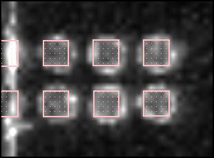
18 Identify Local Registration Features Coarse Trench with CAD Overlay IR View 18


19 Expose Registration Features Error vectors may vary within a field-of-view! 19
20 Register CAD Overlay 20

21 Registered CAD Overlay 21


22 Customized CAD Overlay Digital magnification is used to position milling patterns onto the customized CAD overlay 22
23 Advantages of the Navigational Technique Very accurate Typical errors of ~30 nm over a 150 µm travel range Non-invasive Uses a single high-resolution image No need for live imaging to visit lock points Does not require laser interferometer stage 23
24 Backside Edit Sequence 1. Sample preparation 2. Global navigation a. IR imaging b. Expose corner fiducials 3. Coarse trench 4. Local navigation a. Expose local fiducial(s) b. Adjust CAD overlay 5. Local trench 6. Edit (Blue = next topic) 24
25 Special Considerations Potential problems: Poor visibility Limited IR objective travel range Gas depletion effects Non-planar trench floor Solutions: Reduce aspect ratio Use alternate endpointing techniques (stage current) Set initial Si surface higher than eucentric Use smaller beam currents and/or longer refresh times Optimize milling parameters (may slow down the removal rate) SOI substrates 25
26 Conclusions Full-thickness backside CE is indeed possible Trenching times ~ hour (or better) are possible Successful IR imaging through most samples Accurate navigation using local registration points Particularly well-suited to SOI devices Some challenges exist Reduced visibility Gas depletion effects Economic aspects need further investigation 26
27 Backup Material 27
28 Speed and Trench Planarity Silicon Removal Rate (10 6 µm 3 /min) Pattern Loop Time (msec) Center deeper 28
29 Speed and Trench Planarity Silicon Removal Rate (10 6 µm 3 /min) Pattern Loop Time (msec) Flat bottom 29

30 Speed and Trench Planarity Silicon Removal Rate (10 6 µm 3 /min) Pattern Loop Time (msec) Edges deeper 30
31 Trench with Endpointing Contrast enhanced Top Down View Tilted View 31
2.1. Log on to the TUMI system (you cannot proceed further until this is done).
.") FEI DB235 ex-situ lift out TEM sample preparation procedure Nicholas G Rudawski ngr@ufledu (805) 252-4916 Last updated: 06/19/15 DISCLAIMER: this procedure describes one specific method for preparing ex-situ
FEI DB235 ex-situ lift out TEM sample preparation procedure Nicholas G Rudawski ngr@ufledu (805) 252-4916 Last updated: 06/19/15 DISCLAIMER: this procedure describes one specific method for preparing ex-situ
Scanning Electron Microscopy (FEI Versa 3D Dual Beam)
") Scanning Electron Microscopy (FEI Versa 3D Dual Beam) This operating procedure intends to provide guidance for basic measurements on a standard sample with FEI Versa 3D SEM. For more advanced techniques
Scanning Electron Microscopy (FEI Versa 3D Dual Beam) This operating procedure intends to provide guidance for basic measurements on a standard sample with FEI Versa 3D SEM. For more advanced techniques
Fabrication of Lithium Niobate nanopillars using Focused Ion Beam (FIB)
") Fabrication of Lithium Niobate nanopillars using Focused Ion Beam (FIB) Final report for Nanofabrication with Focused Ion and Electron beams course (SK3750) Amin Baghban June 2015 1- Introduction Thanks
Fabrication of Lithium Niobate nanopillars using Focused Ion Beam (FIB) Final report for Nanofabrication with Focused Ion and Electron beams course (SK3750) Amin Baghban June 2015 1- Introduction Thanks
Wafer Thinning and Thru-Silicon Vias
 Wafer Thinning and Thru-Silicon Vias The Path to Wafer Level Packaging jreche@trusi.com Summary A new dry etching technology Atmospheric Downstream Plasma (ADP) Etch Applications to Packaging Wafer Thinning
UV Nanoimprint Tool and Process Technology. S.V. Sreenivasan December 13 th, 2007
 UV Nanoimprint Tool and Process Technology S.V. Sreenivasan December 13 th, 2007 Agenda Introduction Need tool and process technology that can address: Patterning and CD control Alignment and Overlay Defect
Methodology for Trench Capacitor Etch Optimization using Voltage Contrast Inspection and Special Processing
 Methodology for Trench Capacitor Etch Optimization using Voltage Contrast Inspection and Special Processing 1 Oliver D. Patterson, 1 Xing J. Zhou, 1 Rohit S. Takalkar, 1 Katherine V. Hawkins, 1 Eric H.
Focused Ion Beam System MI4050
 SCIENTIFIC INSTRUMENT NEWS 2016 Vol. 7 SEPTEMBER Technical magazine of Electron Microscope and Analytical Instruments. Technical Explanation Focused Ion Beam System MI4050 Yasushi Kuroda *1, Yoshihisa
Standard Operating Procedure for FEI Helios 660 NanoLab Part I: SEM Version
 Standard Operating Procedure for FEI Helios 660 NanoLab Part I: SEM Version Helios reservations may be made online using the NERCF website. Note: Always wear gloves when venting the system and exchanging
Project TRIPLE-S Microscope: Contribution of AMG Technology Ltd.
 Project TRIPLE-S Microscope: Contribution of AMG Technology Ltd. V. Stavrov, G. Stavreva EUROSTARS ROADSHOW - SOFIA, May 26 th, 2015 1 About AMG Technology Ltd. Company Technology background Project TRIPLE-S
Advanced WLP Platform for High-Performance MEMS. Presented by Dean Spicer, Director of Engineering
 Advanced WLP Platform for High-Performance MEMS Presented by Dean Spicer, Director of Engineering 1 May 11 th, 2016 1 Outline 1. Application Drivers for High Performance MEMS Sensors 2. Approaches to Achieving
FIB Operating Procedure. Effective Date: 08/14/2012 Author(s): Jiong Hua Phone:
: Jiong Hua Phone:") FIB Operating Procedure Effective Date: 08/14/2012 Author(s): Jiong Hua Phone: 402-472-3773 Email: jhua2@unl.edu 1 1 Introduction 1.1 Key Words Focused Ion Beam (FIB), FEI Strata 201, Ion milling 1.2 Purpose
FIB Operating Procedure Effective Date: 08/14/2012 Author(s): Jiong Hua Phone: 402-472-3773 Email: jhua2@unl.edu 1 1 Introduction 1.1 Key Words Focused Ion Beam (FIB), FEI Strata 201, Ion milling 1.2 Purpose
FEI Strata Dual-beam FIB
 FEI Strata Dual-beam FIB Quick start Guide Compiled by Mat t hew Hughes and Tony Chen Page 0 Purpose of this guide INTRODUCTION This quick start guide is meant to provide cursory operational knowledge
Liquid Crystal Display (LCD)
") Liquid Crystal Display (LCD) When coming into contact with grooved surface in a fixed direction, liquid crystal molecules line up parallelly along the grooves. When coming into contact with grooved surface
Liquid Crystal Display (LCD) When coming into contact with grooved surface in a fixed direction, liquid crystal molecules line up parallelly along the grooves. When coming into contact with grooved surface
BTC and SMT Rework Challenges
 BTC and SMT Rework Challenges Joerg Nolte Ersa GmbH Wertheim, Germany Abstract Rising customer demands in the field of PCB repair are a daily occurrence as the rapid electronic industry follows new trends
3D-Nano-Printing via Focused Electron Beams: From a Concept Towards Stable Nano-Fabrication.
 Work Group S 3 Institute of Electron Microscopy and Nanoanalysis Graz Centre for Electron Microscopy 3D-Nano-Printing via Focused Electron Beams: From a Concept Towards Stable Nano-Fabrication. Robert
Screen investigations for low energetic electron beams at PITZ
 1 Screen investigations for low energetic electron beams at PITZ S. Rimjaem, J. Bähr, H.J. Grabosch, M. Groß Contents Review of PITZ setup Screens and beam profile monitors at PITZ Test results Summary
WAFER PROBER MODEL. IR-OBIRCH analysis system Infra Red - Optical Beam Induced Resistance CHange AMOS -200
 WAFER PROBER MODEL IR-OBIRCH analysis system Infra Red - Optical Beam Induced Resistance CHange AMOS -200 IR-OBIRCH Analysis System The μamos is a semiconductor failure analysis system which uses IR-OBIRCH
The hybrid photon detectors for the LHCb-RICH counters
 7 th International Conference on Advanced Technology and Particle Physics The hybrid photon detectors for the LHCb-RICH counters Maria Girone, CERN and Imperial College on behalf of the LHCb-RICH group
University of Minnesota Nano Fabrication Center Standard Operating Procedure
 Equipment Name: Focused Ion Beam (FIB) Coral Name: fib Revision Number: 2 Model: FEI Quanta 200 3D Revisionist: Kevin Roberts Location: Area 3 Date: 9/17/2013 1 Description The Quanta 200 3D is a DualBeam
ABRS Series. Air-Bearing Rotary Stage. Direct-drive, slotless brushless servomotor. Zero cogging motor for outstanding velocity stability
 ABRS Series Air-Bearing Rotary Stage Direct-drive, slotless brushless servomotor Zero cogging motor for outstanding velocity stability Outstanding error motion and wobble performance Direct coupled, high
Technology White Paper Plasma Displays. NEC Technologies Visual Systems Division
 Technology White Paper Plasma Displays NEC Technologies Visual Systems Division May 1998 1 What is a Color Plasma Display Panel? The term Plasma refers to a flat panel display technology that utilizes
Multilevel Beam SOI-MEMS for Optical Applications
 pp. 281-285 Multilevel Beam SOI-MEMS for Optical Applications Veljko Milanović Adriatic Research Institute 2131 University Ave., Suite 322, Berkeley, CA 94704 veljko@adriaticresearch.org Abstract A microfabrication
AFM1 Imaging Operation Procedure (Tapping Mode or Contact Mode)
") AFM1 Imaging Operation Procedure (Tapping Mode or Contact Mode) 1. Log into the Log Usage system on the SMIF web site 2. Open Nanoscope 6.14r1 software by double clicking on the Nanoscope 6.14r1 desktop
AFM1 Imaging Operation Procedure (Tapping Mode or Contact Mode) 1. Log into the Log Usage system on the SMIF web site 2. Open Nanoscope 6.14r1 software by double clicking on the Nanoscope 6.14r1 desktop
RHP-IS DESKTOP IMAGE STABILIZER
 RHP-IS DESKTOP IMAGE STABILIZER Instruction Manual Firmware release 2.1 and above 2005-06-22 Rock2000.com P.O. BOX 4242, Middletown, New York, 10941, USA www.rock2000.com support@rock2000.com 2 Contents
Supplementary Figure 1. OLEDs/polymer thin film before and after peeled off from silicon substrate. (a) OLEDs/polymer film fabricated on the Si
 OLEDs/polymer film fabricated on the Si") Supplementary Figure 1. OLEDs/polymer thin film before and after peeled off from silicon substrate. (a) OLEDs/polymer film fabricated on the Si substrate. (b) Free-standing OLEDs/polymer film peeled off
Supplementary Figure 1. OLEDs/polymer thin film before and after peeled off from silicon substrate. (a) OLEDs/polymer film fabricated on the Si substrate. (b) Free-standing OLEDs/polymer film peeled off
Advanced Sensor Technologies
 Advanced Sensor Technologies Jörg Amelung Fraunhofer Institute for Photonics Microsystems Name of presenter date Sensors as core element for IoT Next phase of market grow New/Advanced Requirements based
Description of task... 2 Sample preparation... 2 Sample insertion and SEM settings... 3 Eucentricity... 4
 These are simple notes taken by Charlie Sanabria while learning how to use the Focused Ion Beam (FIB) in the Scanning Electron Microscope (SEM) at the Applied Superconductivity Center (ASC). The instructions
PRODUCT NEWS FEI LAUNCHES APREO HIGH- PERFORMANCE SEM RENISHAW OFFERS CONFOCAL RAMAN MICROSCOPE
 40 PRODUCT NEWS Larry Wagner, LWSN Consulting Inc. lwagner10@verizon.net FEI LAUNCHES APREO HIGH- PERFORMANCE SEM FEI (Hillsboro, Ore.) announced the new Apreo scanning electron microscope (SEM), offering
Standard Operating Procedure of nanoir2-s
 Standard Operating Procedure of nanoir2-s The Anasys nanoir2 system is the AFM-based nanoscale infrared (IR) spectrometer, which has a patented technique based on photothermal induced resonance (PTIR),
DEEPFRAME BASIC KIT- USER MANUAL VERSION ORIGINAL USER MANUAL
 DEEPFRAME BASIC KIT- USER MANUAL VERSION 1.0 - ORIGINAL USER MANUAL new type of mixed reality display that enables digital content to appear as a hologram on top of reality seen 1 Content Security precautions
DektakXT Profilometer. Standard Operating Procedure
 DektakXT Profilometer Standard Operating Procedure 1. System startup and sample loading: a. Ensure system is powered on by looking at the controller to the left of the computer.(it is an online software,
Reduction of Device Damage During Dry Etching of Advanced MMIC Devices Using Optical Emission Spectroscopy
 Reduction of Device Damage During Dry Etching of Advanced MMIC Devices Using Optical Emission Spectroscopy D. Johnson, R. Westerman, M. DeVre, Y. Lee, J. Sasserath Unaxis USA, Inc. 10050 16 th Street North
High ResolutionCross Strip Anodes for Photon Counting detectors
 High ResolutionCross Strip Anodes for Photon Counting detectors Oswald H.W. Siegmund, Anton S. Tremsin, Robert Abiad, J. Hull and John V. Vallerga Space Sciences Laboratory University of California Berkeley,
Etching Part 2. Saroj Kumar Patra. TFE4180 Semiconductor Manufacturing Technology. Norwegian University of Science and Technology ( NTNU )
") 1 Etching Part 2 Chapter : 16 Semiconductor Manufacturing Technology by M. Quirk & J. Serda Spring Semester 2014 Saroj Kumar Patra, Norwegian University of Science and Technology ( NTNU ) 2 Introduction
1 Etching Part 2 Chapter : 16 Semiconductor Manufacturing Technology by M. Quirk & J. Serda Spring Semester 2014 Saroj Kumar Patra, Norwegian University of Science and Technology ( NTNU ) 2 Introduction
Agilent 86120B, 86120C, 86122A Multi-Wavelength Meters Technical Specifications
 Agilent 86120B, 86120C, 86122A Multi-Wavelength Meters Technical Specifications March 2006 Agilent multi-wavelength meters are Michelson interferometer-based instruments that measure wavelength and optical
Muon Forward Tracker. MFT Collaboration
 Muon Forward Tracker MFT Collaboration QGP France 2013 Introduction Summary of what «physically» MFT looks like: - Silicon detector - Data flow - Mechanical aspects - Power supplies - Cooling - Insertion/Extraction
Development of Ultra-High-Density (UHD) Silicon Photomultipliers with improved Detection Efficiency
 Silicon Photomultipliers with improved Detection Efficiency") Development of Ultra-High-Density (UHD) Silicon Photomultipliers with improved Detection Efficiency Fabio Acerbi, Alberto Gola, Giovanni Paternoster, Claudio Piemonte, Nicola Zorzi http://iris.fbk.eu/silicon-photomultipliers
Development of Ultra-High-Density (UHD) Silicon Photomultipliers with improved Detection Efficiency Fabio Acerbi, Alberto Gola, Giovanni Paternoster, Claudio Piemonte, Nicola Zorzi http://iris.fbk.eu/silicon-photomultipliers
Quick Report on Silicon G-APDs (a.k.a. Si-PM) studies. XIV SuperB General Meeting LNF - Frascati
 studies. XIV SuperB General Meeting LNF - Frascati") Quick Report on Silicon G-APDs (a.k.a. Si-PM) studies XIV SuperB General Meeting LNF - Frascati Report of the work done in Padova Dal Corso F., E.F., Simi G., Stroili R. University & INFN Padova Outline
Quick Report on Silicon G-APDs (a.k.a. Si-PM) studies XIV SuperB General Meeting LNF - Frascati Report of the work done in Padova Dal Corso F., E.F., Simi G., Stroili R. University & INFN Padova Outline
Analog, Mixed-Signal, and Radio-Frequency (RF) Electronic Design Laboratory. Electrical and Computer Engineering Department UNC Charlotte
 Electronic Design Laboratory. Electrical and Computer Engineering Department UNC Charlotte") Analog, Mixed-Signal, and Radio-Frequency (RF) Electronic Design Laboratory Electrical and Computer Engineering Department UNC Charlotte Teaching and Research Faculty (Please see faculty web pages for
Analog, Mixed-Signal, and Radio-Frequency (RF) Electronic Design Laboratory Electrical and Computer Engineering Department UNC Charlotte Teaching and Research Faculty (Please see faculty web pages for
HC9000D. Color : Midnight Black
 HOME CINEMA HC9000D NUEVO HC9000D 2 HC9000D - Videoproyector 0,61" 3-SXRD (16:9 Panorámico) - Resolución Full HD 1920x1080 con visión 3D - Luminosidad 1100 ANSI Lumens - Contraste 150.000:1 - Ratio de
Leveraging 300 mm Technology Solutions to Enable New MEMS Process Capabilities
 Leveraging 300 mm Technology Solutions to Enable New MEMS Process Capabilities Evan Patton Semicon Europa November 2017 Lam Research Corp. 1 Presentation Outline The Internet of Things (IoT) as a market
Overcoming Challenges in 3D NAND Volume Manufacturing
 Overcoming Challenges in 3D NAND Volume Manufacturing Thorsten Lill Vice President, Etch Emerging Technologies and Systems Flash Memory Summit 2017, Santa Clara 2017 Lam Research Corp. Flash Memory Summit
Review Report of The SACLA Detector Meeting
 Review Report of The SACLA Detector Meeting The 2 nd Committee Meeting @ SPring-8 Date: Nov. 28-29, 2011 Committee Members: Dr. Peter Denes, LBNL, U.S. (Chair of the Committee) Prof. Yasuo Arai, KEK, Japan.
CMD GHz Fundamental Mixer
 Features Low conversion loss High isolation Wide IF bandwidth Passive double balanced topology Small die size Functional Block Diagram LO RF 1 2 Description The CMD177 is a general purpose double balanced
Setting Up the Warp System File: Warp Theater Set-up.doc 25 MAY 04
 Setting Up the Warp System File: Warp Theater Set-up.doc 25 MAY 04 Initial Assumptions: Theater geometry has been calculated and the screens have been marked with fiducial points that represent the limits
D-ILA PROJECTOR DLA-G15 DLA-S15
 D-ILA PROJECTOR DLA-G15 Outstanding Projection Im Breakthrough D-ILA projector offers high-contrast 350:1, 1500 ANSI lumen brightness and S-XGA resolution Large-size projection images with all the sharpness
Durham Magneto Optics Ltd. NanoMOKE 3 Wafer Mapper. Specifications
 Durham Magneto Optics Ltd NanoMOKE 3 Wafer Mapper Specifications Overview The NanoMOKE 3 Wafer Mapper is an ultrahigh sensitivity Kerr effect magnetometer specially configured for measuring magnetic hysteresis
Non-Invasive Energy Spread Monitoring for the JLAB Experimental Program via Synchrotron Light Interferometers
 Non-Invasive for the JLAB Experimental Program via Synchrotron Light Interferometers P. Chevtsov, T. Day, A.P. Freyberger, R. Hicks Jefferson Lab J.-C. Denard Synchrotron SOLEIL 20th March 2005 1. Energy
Standard AFM Modes User s Manual
 Standard AFM Modes User s Manual Part #00-0018-01 Issued March 2014 2014 by Anasys Instruments Inc, 325 Chapala St, Santa Barbara, CA 93101 Page 1 of 29 Table of contents Chapter 1. AFM Theory 3 1.1 Detection
SPATIAL LIGHT MODULATORS
 SPATIAL LIGHT MODULATORS Reflective XY Series Phase and Amplitude 512x512 A spatial light modulator (SLM) is an electrically programmable device that modulates light according to a fixed spatial (pixel)
Parameter Min Typ Max Units Frequency Range, RF
 Features Low conversion loss High isolation Ultra wide IF bandwidth Passive double balanced topology Small die size Description The is a general purpose double balanced mixer die with ultra wide IF bandwidth
Spatial Light Modulators XY Series
 Spatial Light Modulators XY Series Phase and Amplitude 512x512 and 256x256 A spatial light modulator (SLM) is an electrically programmable device that modulates light according to a fixed spatial (pixel)
EdiLine III Series Datasheet
 High Power LEDs EdiLine III Series Datasheet The linear structure of EdiLine III Series results in an easier heat dissipation requirement, making versatile fixtures design possible as well as an overall
CMD195. DC-20 GHz SPDT Non-reflective Switch. Features. Functional Block Diagram. Description
 Features Positive gain slope High isolation Fast switching speed Non-reflective design Small die size Functional Block Diagram B A 3 4 5 2 RFC A B 6 Description The is a broadband nonreflective GaAs MMIC
High Power ARNS/IFF Limiter Module: Ultra Low Flat Leakage & Fast Recovery Time
 RELEASED RFLM-961122MC-299 High Power ARNS/IFF Limiter Module: Ultra Low Flat Leakage & Fast Recovery Time Features: SMT Limiter Module: 8mm x 5mm x 2.5mm Frequency Range: 960 MHz to 1,215 MHz High Average
digitile Q FIXED Contact T REV10/ /AC
 digitile Q FIXED THE FIRST GENERATION OF A UNIVERSAL LED TILE SCREEN SYSTEM A new generation of universal LED Tile screen system that has been developed to meet the demands of adaptability. Using a basic
24. Scaling, Economics, SOI Technology
 24. Scaling, Economics, SOI Technology Jacob Abraham Department of Electrical and Computer Engineering The University of Texas at Austin VLSI Design Fall 2017 December 4, 2017 ECE Department, University
Pressure sensor. Surface Micromachining. Residual stress gradients. Class of clean rooms. Clean Room. Surface micromachining
 Pressure sensor Surface Micromachining Deposit sacrificial layer Si PSG By HF Poly by XeF2 Pattern anchors Deposit/pattern structural layer Etch sacrificial layer Surface micromachining Structure sacrificial
PROFESSIONAL D-ILA PROJECTOR DLA-G11
 PROFESSIONAL D-ILA PROJECTOR DLA-G11 A new digital projector that projects true S-XGA images with breakthrough D-ILA technology Large-size projection images with all the sharpness and clarity of a small-screen
Single-Step CMOS Compatible Fabrication of High Aspect Ratio Microchannels Embedded in Silicon
 Delft University of Technology Single-Step CMOS Compatible Fabrication of High Aspect Ratio Microchannels Embedded in Silicon Kluba, Marta; Arslan, Aslihan; Stoute, Ronald; Muganda, James; Dekker, Ronald
Technology Overview LTCC
 Sheet Code RFi0604 Technology Overview LTCC Low Temperature Co-fired Ceramic (LTCC) is a multilayer ceramic substrate technology that allows the realisation of multiple embedded passive components (Rs,
PROFESSIONAL D-ILA PROJECTOR DLA-G11
 PROFESSIONAL D-ILA PROJECTOR DLA-G11 A new digital projector that projects true S-XGA images with breakthrough D-ILA technology Large-size projection images with all the sharpness and clarity of a small-screen
9 rue Alfred Kastler - BP Nantes Cedex 3 - France Phone : +33 (0) website :
 website :") 9 rue Alfred Kastler - BP 10748-44307 Nantes Cedex 3 - France Phone : +33 (0) 240 180 916 - email : info@systemplus.fr - website : www.systemplus.fr January 2012 Written by: Maher SAHMIMI DISCLAIMER :
9 rue Alfred Kastler - BP 10748-44307 Nantes Cedex 3 - France Phone : +33 (0) 240 180 916 - email : info@systemplus.fr - website : www.systemplus.fr January 2012 Written by: Maher SAHMIMI DISCLAIMER :
THE NEW LASER FAMILY FOR FINE WELDING FROM FIBER LASERS TO PULSED YAG LASERS
 FOCUS ON FINE SOLUTIONS THE NEW LASER FAMILY FOR FINE WELDING FROM FIBER LASERS TO PULSED YAG LASERS Welding lasers from ROFIN ROFIN s laser sources for welding satisfy all criteria for the optimized laser
FEI FIB Focused Ion Beam
 Operating Manual Part 1 FEI FIB Focused Ion Beam IF IN DOUBT, ASK 1.00 IF ANYTHING UNUSUAL HAPPENS, OR IF THERE IS ANYTHING YOU ARE UNSURE ABOUT, STOP AND CONTACT ME! DO NOT PROCEED OR ATTEMPT TO FIX THE
Developing an AFM-based Automatic Tool for NanoAsperity Quantification
 Developing an AFM-based Automatic Tool for NanoAsperity Quantification September 18, 2008 Sergey Belikov*, Lin Huang, Jian Shi, Ji Ma, Jianli He, Bob Tench, and Chanmin Su Veeco Instruments Inc., Santa
Large-Scale Polysilicon Surface Micro-Machined Spatial Light Modulator
 Large-Scale Polysilicon Surface Micro-Machined Spatial Light Modulator Clara Dimas, Julie Perreault, Steven Cornelissen, Harold Dyson, Peter Krulevitch, Paul Bierden, Thomas Bifano, Boston Micromachines
R Rxx-Vxxxx-L334-x
 CEZOS 81-534 Gdynia POLAND, Olgierda 88/b tel. +48 58 664 88 61 cezos@cezos.com www.cezos.com Date: 29.08.2016 Revision 1.2 INTRODUCTION RGBW LED module is an advanced light source designed for the best
Requirements for the Beam Abort Magnet and Dump
 Requirements for the Beam Abort Magnet and Dump A beam abort kicker (pulsed dipole magnet) and dump are required upbeam of the LCLS undulator in order to protect the undulator from mis-steered and poor
Tender Notification for the procurement of a "Dual beam (FIB - FE SEM) system" at IISc (Last Date for submission of tenders: 31st March 2016)
 system at IISc (Last Date for submission of tenders: 31st March 2016)") Tender Notification for the procurement of a "Dual beam (FIB - FE SEM) system" at IISc (Last Date for submission of tenders: 31st March 2016) Dear Sir/Madam, Kindly send your best quotation for the following
Tender Notification for the procurement of a "Dual beam (FIB - FE SEM) system" at IISc (Last Date for submission of tenders: 31st March 2016) Dear Sir/Madam, Kindly send your best quotation for the following
KRAMER ELECTRONICS LTD. USER MANUAL
 KRAMER ELECTRONICS LTD. USER MANUAL MODEL: Projection Curved Screen Blend Guide How to blend projection images on a curved screen using the Warp Generator version K-1.4 Introduction The guide describes
These are used for producing a narrow and sharply focus beam of electrons.
 CATHOD RAY TUBE (CRT) A CRT is an electronic tube designed to display electrical data. The basic CRT consists of four major components. 1. Electron Gun 2. Focussing & Accelerating Anodes 3. Horizontal
Standard Operating Procedure II: EDS (Bruker Flat-Quad)
") Standard Operating Procedure II: EDS (Bruker Flat-Quad) ywcmatsci.yale.edu ESC II, Room A119F 810 West Campus Drive West Haven, CT 06516 Version 1.1, October 2018 1 > FOLLOW the SOP strictly to keep the
Standard Operating Procedure II: EDS (Bruker Flat-Quad) ywcmatsci.yale.edu ESC II, Room A119F 810 West Campus Drive West Haven, CT 06516 Version 1.1, October 2018 1 > FOLLOW the SOP strictly to keep the
Connection for filtered air
 BeamWatch Non-contact, Focus Spot Size and Position monitor for high power YAG, Diode and Fiber lasers Instantly measure focus spot size Dynamically measure focal plane location during start-up From 1kW
Mahdad Manavi LOTS Technology, Inc.
 Presented by Mahdad Manavi LOTS Technology, Inc. 1 Authors: Mahdad Manavi, Aaron Wegner, Qi-Ze Shu, Yeou-Yen Cheng Special Thanks to: Dan Soo, William Oakley 2 25 MB/sec. user data transfer rate for both
Spatial Light Modulators
 Spatial Light Modulators XY Series -Complete, all-in-one system Data Sheet November 2010 Spatial Light Modulators A spatial light modulator (SLM) is an electrically programmable device that modulates light
Light-Emitting Diodes
 445.664 Light-Emitting Diodes Chapter 1. History of Light-Emitting Diodes Euijoon Yoon Light Emitting Diodes (LEDs) There are two major technologies : - All-semiconductor-based illumination devices - Semiconductor/phosphor
Module 1: Digital Video Signal Processing Lecture 3: Characterisation of Video raster, Parameters of Analog TV systems, Signal bandwidth
 The Lecture Contains: Analog Video Raster Interlaced Scan Characterization of a video Raster Analog Color TV systems Signal Bandwidth Digital Video Parameters of a digital video Pixel Aspect Ratio file:///d
DEEPFRAME BASIC KIT- USER MANUAL VERSION ORIGINAL USER MANUAL
 DEEPFRAME BASIC KIT- USER MANUAL VERSION 1.3 - ORIGINAL USER MANUAL It is important to read this manual before using the DeepFrame, and to follow advices and instructions on safety, operation and general
Product Presentation Digital Cinema Systems
 Product Presentation Digital Cinema Systems Projectors and related products explanations and comparisons Overview Digital Projector Family DCP 30 SX II with pedestal DCP 30 MX II with pedestal DCP 30 LX
Computer Graphics Hardware
 Computer Graphics Hardware Kenneth H. Carpenter Department of Electrical and Computer Engineering Kansas State University January 26, 2001 - February 5, 2004 1 The CRT display The most commonly used type
Spatial Light Modulators
 Spatial Light Modulators XY Series -Complete, all-in-one system Data Sheet May 2009 Spatial Light Modulators A spatial light modulator (SLM) is an electrically programmable device that modulates light
Luxon is a worldwide, high-tech enterprise specializing in the design, production and sales of LED encapsulation, LED displays and LED modules.
 Managing Director Peter Economou 0410 575 677 Peter@LuxonLED.com.au Managing Director Jamie Croudace 0466 245 471 Jamie@LuxonLED.com.au Luxon is a worldwide, high-tech enterprise specializing in the design,
Standard Operating Manual
 Standard Operating Manual LAM490 AutoEtch System Copyright 11.2015 by Hong Kong University of Science & Technology. All rights reserved. Page 1 Contents 1. Picture and Location 2. Process Capabilities
Advances in Roll-to-Roll Imprint Lithography for Display Applications Using Self Aligned Imprint Lithography. John G Maltabes HP Labs
 Advances in Roll-to-Roll Imprint Lithography for Display Applications Using Self Aligned Imprint Lithography John G Maltabes HP Labs Outline Introduction Roll to Roll Challenges and Benefits HP Labs Roll
B-AFM. v East 33rd St., Signal Hill, CA (888)
") B-AFM The B-AFM is a basic AFM that provides routine scanning. Ideal for scientists and educators, the B-AFM is capable of creating high-resolution topography images of nanostructures in standard scanning
B-AFM The B-AFM is a basic AFM that provides routine scanning. Ideal for scientists and educators, the B-AFM is capable of creating high-resolution topography images of nanostructures in standard scanning
Semiconductors Displays Semiconductor Manufacturing and Inspection Equipment Scientific Instruments
 Semiconductors Displays Semiconductor Manufacturing and Inspection Equipment Scientific Instruments Electronics 110-nm CMOS ASIC HDL4P Series with High-speed I/O Interfaces Hitachi has released the high-performance
Deep Silicon Etch Technology for Advanced MEMS Applications
 Deep Silicon Etch Technology for Advanced MEMS Applications Shenjian Liu, Ph.D. Managing Director, AMEC AMEC Company Profile and Product Line-up AMEC HQ, R&D and MF Facility in Shanghai AMEC Taiwan AMEC
High aspect ratio deep RIE for novel 3D radiation sensors in high energy physics applications
 High aspect ratio deep RIE for novel 3D radiation sensors in high energy physics applications Angela Kok, Thor-Erik Hansen, Trond Hansen, Geir Uri Jensen, Nicolas Lietaer, Michal Mielnik, Preben Storås
ASMT UxB5 Nxxxx Surface Mount LED Indicator
 ASMT UxB5 Nxxxx Surface Mount LED Indicator Description This family of SMT LEDs is packaged in the industry standard PLCC 2 package. These SMT LEDs have high reliability performance and are designed to
PanelView 1400e CRT Maintenance
 Release Note PanelView 1400e CRT Maintenance Maximizing the life of your PanelView 1400e, CRT Terminals To maximize the life of a CRT, the following is strongly recommended: Adjust the external brightness
Spiider THE NEXT BIG THING FROM ROBE!
 Spiider THE NEXT BIG THING FROM ROBE! Spiider, a superbright next generation of LED WashBeam luminaires, using 18x 30 Watt and 1x 60 Watt LEDs and combining it with a very efficient 12,5:1 zoom optical
Nano-Imprint Lithography Infrastructure: Imprint Templates
 Nano-Imprint Lithography Infrastructure: Imprint Templates John Maltabes Photronics, Inc Austin, TX 1 Questions to keep in mind Imprint template manufacturability Resolution Can you get sub30nm images?
Planar LookThru OLED Transparent Display. Content Developer s Guide. 1 TOLED Content Developer s Guide A
 Planar LookThru OLED Transparent Display Content Developer s Guide 1 TOLED Content Developer s Guide 020-1316-00A Table of Contents How Transparent OLED Works... 3 History and Definitions... 3 Pixel Structure...
GENCOA Key Company Facts. GENCOA is a private limited company (Ltd) Founded 1995 by Dr Dermot Monaghan. Located in Liverpool, UK
 Founded 1995 by Dr Dermot Monaghan. Located in Liverpool, UK") GENCOA Key Company Facts GENCOA is a private limited company (Ltd) Founded 1995 by Dr Dermot Monaghan Located in Liverpool, UK Employs 34 people 6 design (Pro E 3D CAD) 4 process development & simulation
GENCOA Key Company Facts GENCOA is a private limited company (Ltd) Founded 1995 by Dr Dermot Monaghan Located in Liverpool, UK Employs 34 people 6 design (Pro E 3D CAD) 4 process development & simulation
DESIGN OF VISIBLE LIGHT COMMUNICATION SYSTEM
 DESIGN OF VISIBLE LIGHT COMMUNICATION SYSTEM *Vishakh B V, **Mohammed Kamal Khwaja *School of Electronics Engineering, VIT University, Vellore, India ** School of Electronics Engineering, VIT University,
EVALUATION KIT AVAILABLE +3.0V to +5.5V, 125Mbps to 266Mbps Limiting Amplifiers with Loss-of-Signal Detector V CC FILTER.
 19-1314; Rev 5; 8/06 EVALUATION KIT AVAILABLE +3.0V to +5.5V, 125Mbps to 266Mbps General Description The MAX3969 is a recommended upgrade for the MAX3964 and MAX3968. The limiting amplifier, with 2mVP-P
Automatic Defect Recognition in Industrial Applications
 Automatic Defect Recognition in Industrial Applications Klaus Bavendiek, Frank Herold, Uwe Heike YXLON International, Hamburg, Germany INDE 2007 YXLON. The reason why 1 Different Fields for Usage of ADR
Abstract. Keywords INTRODUCTION. Electron beam has been increasingly used for defect inspection in IC chip
 Abstract Based on failure analysis data the estimated failure mechanism in capacitor like device structures was simulated on wafer in Front End of Line. In the study the optimal process step for electron
Advancements in Acoustic Micro-Imaging Tuesday October 11th, 2016
 Central Texas Electronics Association Advancements in Acoustic Micro-Imaging Tuesday October 11th, 2016 A review of the latest advancements in Acoustic Micro-Imaging for the non-destructive inspection