AN-1200 True Random Number Generator Hardware
|
|
|
- Anissa Leonard
- 6 years ago
- Views:
Transcription

1 AN-1200 True Random Number Generator Hardware In cryptographic applications such as key generation and signing, there is a need for random numbers. There are many methods which hardware or firmware can use to generate pseudorandom numbers. However, pseudo-random number generators are deterministic: if the internal state of the generator is known, then the output of the generator is entirely predictable. This makes pseudo-random number generators inappropriate for cryptographic applications. These applications require a true random number generator (TRNG). A TRNG uses unpredictable physical phenomena to generate random numbers. An example of a TRNG would be to amplify thermal noise from a resistor, then use an analog-to-digital convertor to convert this noise into numbers. Such a system usually requires a lot of discrete components due to the large gain needed. Because thermal noise is the result of chaotic microscopic effects, this generator will generate unpredictable numbers. This unpredictability is referred to as entropy. Entropy can be measured in bits, for example, a fair coin toss will produce 1 bit of entropy, as there are two equally possible outcomes. Independent sources of entropy add, so tossing 8 independent, fair coins will produce 8 bits of entropy. A biased coin that always lands on heads will produce 0 bits of entropy, since a fully biased coin is completely predictable. A good TRNG will be able to quickly generate enough bits of entropy, so that cryptographic keys or secrets cannot be feasibly guessed. A bad random number generator can compromise a cryptographic system. For example, a faulty random number generator was the cause of several thefts of the cryptocurrency Bitcoin [1]. Entropy source The true random number generator described in this application note uses free-running ring oscillators. These ring oscillators are constructed using an odd number of inverters constructed out of LUTs. The oscillators are free-running in the sense that they are not locked to other clocks, and will accumulate jitter see Figure 1 for a frequency-domain representation of the jitter from a single oscillator. This jitter is a result of many unpredictable effects, including thermal noise, so a generator constructed out of ring oscillators is justified in being called a true random number generator. Figure 1. FFT of the output of a single ring oscillator implemented in a GreenPAK device. This ring oscillator oscillates at a nominal frequency of about 19 MHz, and the output has been digitally sampled at 48 kbit/s. Because the oscillator s frequency is far above the Nyquist frequency, the oscillator signal has been aliased to ~7.5 khz. The jitter in this ring oscillator is visible, as the peak is not infinitely thin, as would be the case for an ideal, jitter-free oscillator. Instead, the peak has a 3 db bandwidth of about 2 khz.

2 To increase the amount of entropy available, and to make the design more robust, many ring oscillators should be used. Because the oscillators are independent, they will randomly drift in and out of phase of each other. The oscillators can be sampled by periodically taking the XOR of all their outputs, which represents the oscillators relative phase. This is not the most efficient way to sample oscillators, as many oscillations are required before the oscillators will drift out of phase with each other. However, it is a simple method that does not require the use of many ring oscillators a higher-throughput design could require over 100 oscillators [2]. Whitening A perfect entropy source generates a stream of bits which have a white power spectrum (equal power in all frequencies; the spectrum is flat) and which are statistically unbiased (nearly equal ones and zeroes). Real entropy sources are imperfect they generate a bitstream which is statistically poor in some way. For example, noise in circuits often has a power spectrum which is not white. Indeed, Figure 1 shows that the ring oscillators used in this application note have a noise power spectrum which is not flat. Asymmetries in a circuit (e.g. due to a difference in rising and falling propagation delays) could cause the output to become biased. Statistically imperfect entropy sources are still useful, but they require post-processing. This post-processing is referred to as whitening. To illustrate the need for whitening, imagine that someone wishes to extract entropy from a series of coin tosses. They are using a hypothetical set of 16 coins 8 of which are fair, 8 of which are completely biased, and will always land on heads. For the sake of analogy, this hypothetical person is also unable to distinguish the fair coins from the biased coins. Flipping all 16 of these coins will lead to a partially predictable result, as there are guaranteed to be at least 8 heads appearing. However, there should still be a total of 8 bits of entropy. A whitener can be used to take the results of the 16 coin tosses, and process these results to obtain 8 random bits. Figure 2. Example of a 4-bit LFSR, implemented using 4 D flip flops and a XOR gate (this particular LFSR is only an example; it is not used in the TRNG implementation). This LFSR will produce the following output: Inspection of this pseudo-random bitstream reveals that it repeats every 15 bits. The whitener used in this application note is a linear feedback shift register (LFSR). A LFSR is easy to construct in hardware and consists of a shift register, with some of the register contents XORed together and fed back into the input of the shift register see Figure 2 for an example of this. On its own, the output of a LFSR will be a repeating pseudo-random sequence of bits. Careful choice of what registers to XOR together means that the cycle length of this pseudo-random sequence will be of maximal cycle length. The maximum possible cycle length of a n-bit shift register is 2 n 1. A table of the suitable XOR choices is given in [3]. A large, maximal LFSR will produce a bitstream which is unbiased and white. A LFSR will produce a bitstream with good statistical properties, but on its own, it is still only pseudo-random. For this application note, the feedback of the LFSR is also XORed with the raw output of the ring oscillators. The LFSR s internal state will now be influenced by the ring oscillators, converting the LFSR from a pseudo-random number generator into a true random number generator. Even with this modification, the overall feedback structure of a large, maximal LFSR ensures that its output is still unbiased and white. Hence an LFSR, used in this way, fulfils the function of a whitener.


3 Realization with GreenPAK designer: ring oscillators Figure 3. Ring oscillator implementations. The top image shows the four oscillators implemented on the matrix 0 side. The bottom image shows the two oscillators implemented on the matrix 1 side. There are enough LUTs in the SLG46620V for six ring oscillators. Their implementation is shown in Figure 3. Each ring oscillator starts with a NAND gate instead of a simple inverter. Connected to each NAND gate is a global enable signal (net EN0 for matrix 0, net EN1 for matrix 1). When this enable signal is low, all the NAND gates will output high, regardless of the state of the other input. This will cause the ring oscillators to stop oscillating and enter a static, well-defined state. When this enable signal is high, the NAND gate effectively functions as another inverter. All the ring oscillators are constructed out of 3 inverters, except for one of the rings, which has an extra buffer. All the rings are constructed out of unique combinations of 2-bit LUTs, 3-bit LUTs, 4- bit LUTs, and the INV0/INV1 blocks. This is a crucial design choice. Experimentation has revealed that if any two rings are constructed out of the same types of blocks, they will have very similar oscillation frequencies. The frequencies are so similar, that small amounts of crosstalk between the oscillators (probably a result of switching noise) will eventually cause the oscillators to phase-lock together. This phenomenon (generally referred to as injection locking) will cause a catastrophic failure in entropy generation, as the oscillators will constantly be exactly in phase with each other. 2-bit LUTs, 3-bit LUTs, 4-bit LUTs, and the INV0/INV1 blocks all have different propagation delays, so using unique combinations of these types of blocks guarantees that the oscillator frequencies will be different. The output of each ring oscillator is latched on the rising edge of the RAW_CLK signal. This follows the advice of [4], where it was observed that failing to latch oscillator outputs causes setup and hold time violations on the input to XOR gates. This approach also helps to reduce switching noise, minimizing the amount of harmful crosstalk between oscillators. Each ring oscillator was measured to have a spectrum like that shown in Figure 1, with a noise bandwidth of about 2 khz. The rate of entropy can be calculated using Hartley s law:
 results in a bitrate of 4 kbit/s. Hence each ring oscillator contributes 4 kbit/s of entropy.")

4 where C is the bitrate, B is the bandwidth and M is the number of distinguishable states. Using B = 2 khz, and M = 2 (since the output of a ring oscillator is either a 0 or a 1) results in a bitrate of 4 kbit/s. Hence each ring oscillator contributes 4 kbit/s of entropy. Finally, the latched outputs of all oscillators are XORed together, to measure their relative phase. This XOR output is latched on the rising edge of the RAW_CLK signal, to ensure that that there are no spurious transitions in the output signal. This results in the RAW_OUT signal. RAW_OUT is sent out of pin 19 for the user. The choice of pin 19 for RAW_OUT was completely arbitrary; system designers are free to re-assign pins to make PCB routing easier. Realization with GreenPAK designer: LFSR Figure 4. LFSR implementation. The top image shows the portion of the LFSR in matrix 0. The bottom image shows the portion of the LFSR in matrix 1. It was necessary to split the LFSR across matrices to fully use both pipe delay blocks. A 35-bit LFSR was implemented, because there exists a maximal 35-bit LFSR with a very simple structure: the feedback consists of the XOR of registers 33 and 35 (see the n=35 entry of Table 3 in [3]). The LFSR uses both pipe delay blocks in the SLG46620V, where each pipe delay block consists of 16 D flip flops in serial. Pipe delay 0 contributes the first 16 bits of the shift register, pipe delay 1 contributes the next 16 bits, and D flip flops 7, 8, and 9 form the last three bits of the shift register. The resulting 35-bit LFSR has a cycle period of 235 1, which is extremely long compared to the LFSR clock rate. The feedback element shown in Figure 4 uses NXOR instead of XOR. This does not change the structure of the LFSR, or the cycle period. However, it does ensure that the LFSR does not enter a lock-up state (where cycle period = 1) when the shift register is initialized to an all-0s state, which is the case during power-on. The LFSR is clocked/shifted by the global LFSR_CLK signal (net LFSR_CLK0 for matrix 0, net LFSR_CLK1 for matrix 1). The output of the LFSR (LFSR_OUT) is not directly exposed to the user. Instead, the output of the LFSR is latched on the rising edge of the WHITE_CLK signal. Note that WHITE_CLK runs at a slower rate than LFSR_CLK this is to allow some bits of LFSR_OUT to be discarded. This latched output is sent to pin 5, as the WHITENED_OUT signal. Like with RAW_OUT, the choice of pin 5 was completely arbitrary.

5 Realization with GreenPAK designer: clocks Figure 5. Clock structure of TRNG. The top image shows the portion in matrix 0. The bottom image shows the portion in matrix 1. The master clock source for the TRNG is a ring oscillator constructed out of LUTs, visible in the bottom image of Figure 5. Although the SLG46620V does have many in-built clocks, none of those were used. The reason for this was to improve rejection against common-mode interference such as power supply noise, temperature variations, and power supply voltage variations. By constructing the master clock in the same way as the entropy source, these common-mode interference sources should affect both the master clock and the entropy source in the same way, partially cancelling out the effect of the interference. The master clock is fed into matrix 1 s EXT. CLK2, where CNT7 and CNT8 are set up as counters to divide the master clock by 306, to achieve a nominal (at VDD = 3.3 V) RAW_CLK of about 80 khz. CNT7 and CNT8 are set up in this particular cascade (CNT7 has counter data = 152, CNT8 has counter data = 1) to ensure that RAW_CLK has a duty cycle of 50%. RAW_CLK is used as the sampling clock for the ring oscillators, hence RAW_OUT will have a nominal bitrate of 80 kbit/s. RAW_CLK is also output to pin 20 (this pin assignment is arbitrary) so that the user can sample RAW_OUT at the right times. LFSR_CLK has the same frequency as RAW_CLK the only difference is that LFSR_CLK can be suppressed by asserting ENABLE_WHITENED low. LFSR_CLK is used to clock the shift registers in the LFSR. In matrix 0, LFSR_CLK is fed into EXT. CLK1, so that CNT5 and CNT6 can derive WHITE_CLK from it. CNT5 and CNT6 are set up as counters, both with counter data = 1, so they divide LFSR_CLK by 4. The divided clock, WHITE_CLK, is used to decimate the LFSR output. WHITE_CLK is sent to pin 3 (this pin assignment is arbitrary) so that the user can sample WHITENED_OUT at the right times. WHITE_CLK has a nominal frequency of 20 khz; WHITENED_OUT has a bitrate of 20 kbit/s. The final bitrate of 20 kbit/s was chosen because testing revealed that each ring oscillator could provide about 4 kbit/s of entropy. Since the entropy source consists of six ring oscillators (see Figure 3), and assuming the entropy sources add, there should be a total of about 24 kbit/s of entropy in RAW_OUT. This is derated to 20 kbit/s to account for imperfections in the ring oscillators and LFSR. Note that while RAW_OUT has a nominal bitrate of 80 kbit/s, the expected entropy rate of RAW_OUT is only 20 kbit/s. This is because RAW_OUT is expected to have statistical imperfections which make its bitstream partially predictable. On the other hand, WHITENED_OUT is completely unpredictable, hence it has a nominal bitrate (of 20 kbit/s) equal to its expected entropy rate.


6 The output of DLY2 holds CNT5 in reset; the DISABLE_WHITENED signal halts WHITE_CLK. DLY2 is set up so that the falling edge of the DISABLE_WHITENED signal is delayed by 400 counts of LFSR_CLK. The effect of this is that after the whitened output is enabled, the first 400 bits of the LFSR will be discarded. It is necessary to discard the first 400 bits of LFSR output so that fresh entropy can mix into the LFSR s internal state. Realization with GreenPAK designer: enable logic Figure 6. Enable logic of TRNG. The left image shows the portion in matrix 0. The right image shows the portion in matrix 1. The remaining configuration is dedicated to enable logic. The enable logic allows the user to save power by disabling sections of the TRNG. The ENABLE_ALL signal is connected to pin 17 (this pin assignment is arbitrary). If the user asserts pin 17 low, then all ring oscillators will stop oscillating. This will cause the entire TRNG to enter a static state. The ENABLE_ALL signal is also ANDed with the output of the POR block. This is necessary, as the ring oscillators will not begin oscillating unless they begin from a well-defined state. The POR clock is configured to output high 4 µs after power-on. This gives the ring oscillators 4 µs to settle into the well-defined disabled state (see the section Realization with GreenPAK designer: ring oscillators ), ensuring that the ring oscillators will reliably start oscillating after power-on. The ENABLE_WHITENED signal is connected to pin 15 (this pin assignment is arbitrary). If the user asserts pin 15 low, then LFSR_CLK will be disabled, and the entire LFSR section will enter a lowpower static state. A related signal, DISABLE_WHITENED, is used to suppress the first 100 bits of whitened output (i.e. the first 400 bits of LFSR output), so that fresh entropy is mixed into the LFSR internal state before anything is output. For this reason, DISABLE_WHITENED will be asserted high whenever the LFSR or entropy source is (re)started. Test results The TRNG described in this application note was implemented in a SLG46620V, and samples were taken from the RAW_OUT and WHITENED_OUT pins. This was done using a LPC11U24 microcontroller that was set up to sample RAW_OUT/WHITENED_OUT on the falling edge of RAW_CLK/WHITENED_CLK. These samples were sent to a PC over a UART-to-USB converter, and the samples were logged into a file for later analysis. The result of an FFT performed on the raw output is shown in Figure 7. While the spectrum is approximately flat, to within 2.5 db, there is clearly a structure of peaks and troughs. This structure is inconsistent with the expected result of a perfect entropy source (a flat spectrum).
 variance observed to be within 0.4 db. Figure 8. FFT results of about 3 million bits of whitened output (sampled from WHITENED_OUT).")
![The spectrum is flat (white). The observed variance is statistical in nature. Further statistical testing can be done using a suite of statistical tests developed by NIST, described in detail in [5].](/docs-images/71/66106578/images/7-1.jpg "For a brief explanation of what each test is examining, see [8]. The NIST tests are specifically adapted to testing random bitstreams.")
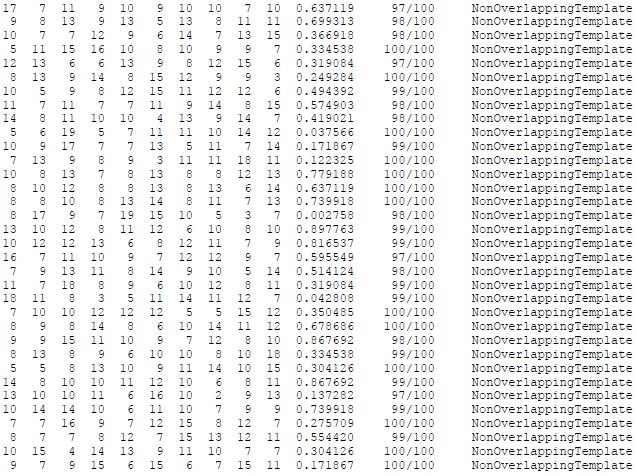
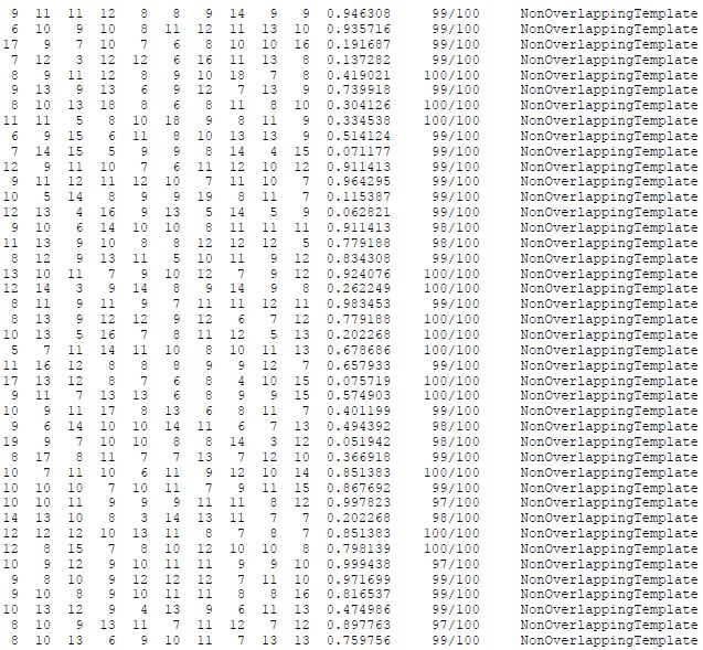
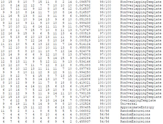
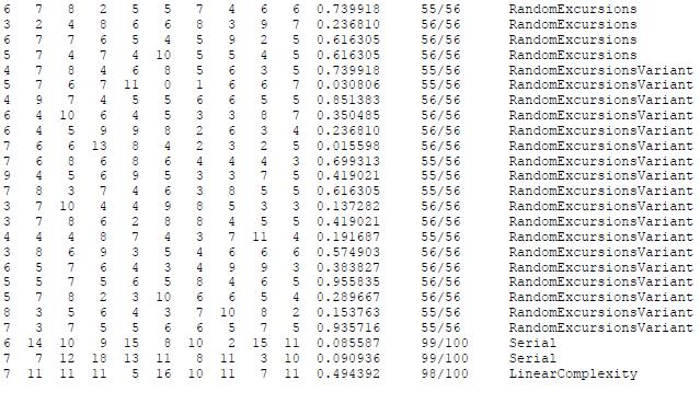
7 Figure 7. FFT results of about 3 million bits of raw output (sampled from RAW_OUT). Wide peaks and troughs in the spectra are clearly visible. The result of an FFT performed on the whitened output is shown in Figure 8. This spectrum is flat, with the (statistical) variance observed to be within 0.4 db. Figure 8. FFT results of about 3 million bits of whitened output (sampled from WHITENED_OUT). The spectrum is flat (white). The observed variance is statistical in nature. Further statistical testing can be done using a suite of statistical tests developed by NIST, described in detail in [5]. For a brief explanation of what each test is examining, see [8]. The NIST tests are specifically adapted to testing random bitstreams. For example, the Frequency test examines whether the proportion of ones and zeroes is the same i.e. the Frequency test checks that the bitstream is unbiased. To test the TRNG, about 80,000,000 bits of RAW_OUT and WHITENED_OUT were collected and recorded in files. These files were split into 100 bitstreams of 800,000 bits each, and then analysed, using the assess tool described in [5]. Appendix A contains the final results ( finalanalysisreport.txt ) for the raw output, and Appendix B contains the final results for the whitened output. An accessible introduction to interpreting the NIST test results is given in [7]. The NIST test results contain a lot of columns, but the important ones are the P-VALUE and PROPORTION columns. Values in the P-VALUE column should be uniformly distributed between 0 and 1. Values close to 0 (e.g ) or 1 (e.g ) are indicative of failure. The PROPORTION column describes how many of the 100 bitstreams passed the statistical tests. Statistically, some of the bitstreams are expected to fail. The minimum pass rate is described at the bottom of each appendix. Asterisks in either the P-VALUE or PROPORTION columns are indicative of failure. The general conclusion from the NIST test results is that the raw output fails most of the statistical tests. This failure is expected the raw output is an imperfect source of entropy. On the other hand, the whitened output passes every statistical test. This indicates that the whitened output can be used as a source of almost-perfectly random bits. How to use the TRNG The TRNG implemented in this application note requires only the SLG46620V to generate the random bitstream; it does not require any external components, except for decoupling capacitors for the SLG46620V. The raw output can be sampled by connecting RAW_CLK (pin 20) and
8 RAW_OUT (pin 19) to a microcontroller see Figure 9 for an example of what these signals look like. If the microcontroller supports SPI in slave mode, then RAW_CLK can be connected to SCLK and RAW_OUT can be connected to MOSI, with CPOL set to 0 and CPHA set to 1 (SPI mode 1). Alternatively, the microcontroller can be set up to interrupt on the falling edge of RAW_CLK, with the interrupt handler sampling RAW_OUT. The whitened output can be similarly sampled using the WHITENED_CLK (pin 3) and WHITENED_OUT (pin 5) signals see Figure 9 for an example of what these signals looks like. The whitened output is the most appropriate output for most applications. Figure 9. Timing diagram showing an example of what the output signals look like. RAW_OUT transitions on the rising edge of RAW_CLK; WHITENED_OUT transitions on the rising edge of WHITENED_CLK. Both RAW_OUT and WHITENED_OUT should be sampled on the falling edge of their respective clocks. In this example, RAW_OUT is depicted as outputting the bitstream , and WHITENED_OUT is depicted as outputting the bitstream RAW_CLK runs at a nominal rate of 80 khz; WHITENED_CLOCK runs at a quarter of RAW_CLK, at a nominal rate of 20 khz. The whitened output can be disabled by asserting ENABLE_WHITENED (pin 15) low. The entire TRNG can be disabled by asserting ENABLE_ALL (pin 17) low. Both enable pins are pulled-up, so if they are both left unconnected, all sections of the TRNG will be enabled. A summary of signals is given in Table 1. Name Pin Type Description RAW_OUT 19 Digital push-pull output RAW_CLK 20 Digital push-pull output WHITENED_OUT 5 Digital push-pull output WHITENED_CLK 3 Digital push-pull output ENABLE_ALL 17 Digital input with pull-up ENABLE_WHITENED 15 Digital input with pull-up Raw output of the TRNG the latched output of the XOR of all ring oscillators, representing their relative phase. Sampling clock for RAW_OUT. Runs at a nominal 80 khz. RAW_OUT transitions on the rising edge of this clock. Output of the TRNG after whitening by a LFSR. Sampling clock for WHITENED_OUT. Runs at a nominal 20 khz. WHITENED_OUT transitions on the rising edge of this clock. When low, stops all clocks within the TRNG, putting it into a low-power static state; RAW_CLK and WHITENED_CLK will stop ticking. When low, stops the LFSR clock, causing the whitened output to halt; WHITENED_CLK will stop ticking. Security considerations Table 1. Summary of TRNG signals High-security applications should verify that the entropy source is working properly. To do this, they must not test the whitened output; the whitened output should not be trusted to be truly random, even if it passes statistical tests. This is because the maximal 35-bit LFSR used in this application note is a good pseudo-random number generator, and will produce results that will pass most statistical tests, even if the entropy source is completely broken. Instead, applications should try to detect failure by running statistical tests on the raw output. For example, applications could
9 test for unusually long strings of 0s or 1s, or use a FFT to test if the raw output spectrum is less flat than Figure 7. For simplicity, the whitened output can be used directly in cryptographic operations. Applications demanding greater security should use the whitened output to seed a cryptographically-secure pseudo-random number generator (CSPRNG), continually reseeding the CSPRNG as new whitened output bits become available. This approach has the advantages: The CSPRNG can be used to generate a high throughput of on-demand bits; the application won t be limited to the 20 kbit/s produced by this TRNG. The reseeding operation allows entropy to accumulate in the CSPRNG s internal state. This guarantees that the CSPRNG will become increasingly unpredictable (and hence secure) over time, even in the event of partial failure of the TRNG s entropy source. Other entropy sources (e.g. data from radio receivers) can be used to reseed the CSPRNG. This will make the cryptographic system more robust against failure of an entropy source. A cryptographic system using a SLG46620V as a TRNG is trivially vulnerable to invasive attacks. An attacker who has physical access to the system can simply remove the SLG46620V, replacing it with a device that produces a completely predictable bitstream. This can be countered by making physical access difficult, or attempting to detect physical access. TRNGs based on ring oscillators are known to be vulnerable to signals injected to their power supply [6]. This can be countered by filtering the power supply. A possible extension to this application note is to use the ACMP and VREF blocks to detect such injection attacks. Downsizing the design The TRNG design described in this application note can be implemented in a smaller GreenPAK, to reduce costs and board space requirements. The number of ring oscillators used in the entropy source could be reduced, down to a minimum of two. Since there are three times fewer oscillators being used, this would reduce the throughput of the design to a third: approximately 6.6 kbit/s. D flip flop requirements could be reduced by using a smaller LFSR for a whitener. The minimum LFSR size depends on the number of ring oscillators, and on the oscillator sampling clock rate. The minimum LFSR size can be experimentally determined by using successively smaller LFSR lengths, until the whitened output begins to fail the NIST statistical tests. Usually, a TRNG is used in a system that contains a microcontroller. Thus, a minimal GreenPAK design could omit the whitener completely, relying on the microcontroller to perform whitening. The firmware in that microcontroller could easily implement a very large LFSR, or it could use a cryptographic hash function to implement a more robust whitener. Conclusion GreenPAK can be used to implement a compact true random number generator that requires no external components (except for decoupling capacitors), and generates true random numbers at a rate of 20 kbit/s. The TRNG has a simple interface, and has power-saving features, making it ideal for mobile, space-constrained devices that require an entropy source for cryptographic operations. References 1. D. Gilson, Blockchain.info issues refunds to bitcoin theft victims, Aug. 21, [Online]. Available: [Accessed: Jun. 30, 2017]. 2. B. Sunar, W. J. Martin, and D. R. Stinson, A Provably Secure True Random Number Generator with Built-In Tolerance to Active Attacks, IEEE Trans. Comput., vol. 56, no. 1, Jan P. Alfke, Efficient Shift Registers, LFSR Counters, and Long Pseudo-Random Sequence Generators, Xilinx Application Note, XAPP 052, Jul. 7, K. Wold, and C. H. Tan, Analysis and Enhancement of Random Number Generator in FPGA Based on Oscillator Rings, Int. J. of Reconfigurable Computing, vol. 2009, article ID , A. Rukhin, J. Soto, J. Nechvatal, M. Smid, E. Barker, S. Leigh, M. Levenson, M. Vangel, D. Banks, A. Heckert, J. Dray, and S. Vo, A Statistical Test Suite for Random and Pseudorandom

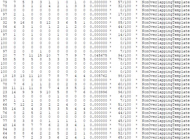
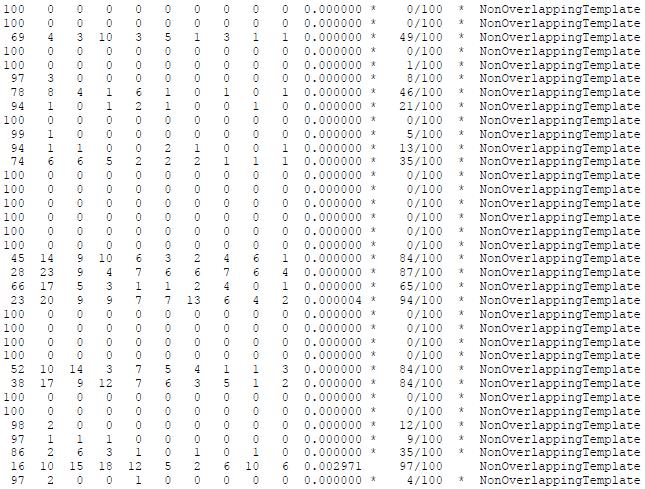
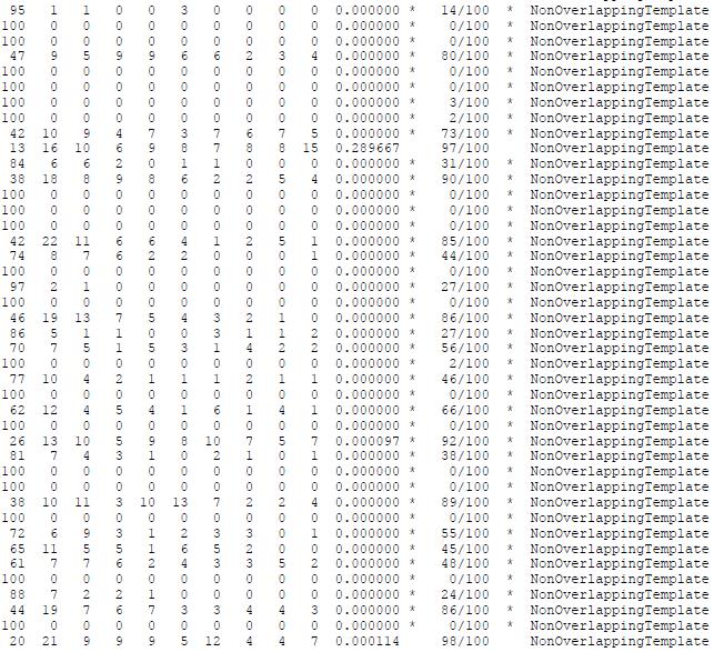
10 Number Generators for Cryptographic Applications, NIST Special Publication , revision 1a, Apr A. T. Markettos, and S. W. Moore, The Frequency Injection Attack on Ring-Oscillator-Based True Random Number Generators, in Proc. 11th Int. Workshop Cryptographic Hardware and Embedded Syst., Lausanne, Switzerland, 2009, pp Interpretation of the results of NIST (p)nrg suite, Jan. 9, [Online]. Available: [Accessed: Jul ]. 8. Guide to the statistical tests, Jul. 16, [Online]. Available: [Accessed: Jul ]. Appendix A: NIST SP test results for raw output For testing methodology and interpretation of results, see the Test results section.
11
12
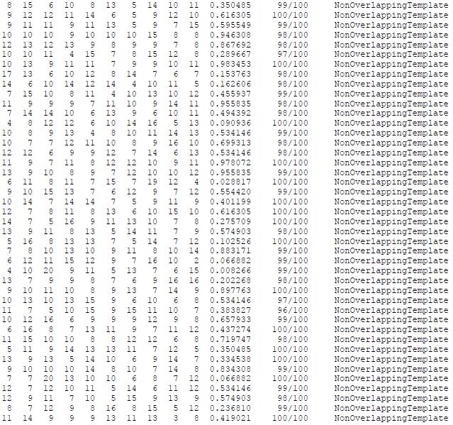
13 Appendix B: NIST SP test results for whitened output For testing methodology and interpretation of results, see the Test results section.
14
15
16
17 About the Author Name: Chris Chua Background: Chris Chua received a Bachelor of Science and Bachelor of Computer Science from Monash University in He is currently working as a part-time teaching assistant at Monash University, and as a freelance electronics engineer and programmer. His interests include physics, microcontrollers, and cryptography. Contact: appnotes@silego.com Files AN-1200 True Random Number Generator Hardware.gp4- (60 KB) AN-1200 True Random Number Generator Hardware.pdf- (1.0 MB) AN-1200.zip- (815 KB) See full list of Application Notes
True Random Number Generation with Logic Gates Only
 True Random Number Generation with Logic Gates Only Jovan Golić Security Innovation, Telecom Italia Winter School on Information Security, Finse 2008, Norway Jovan Golic, Copyright 2008 1 Digital Random
NH 67, Karur Trichy Highways, Puliyur C.F, Karur District UNIT-III SEQUENTIAL CIRCUITS
 NH 67, Karur Trichy Highways, Puliyur C.F, 639 114 Karur District DEPARTMENT OF ELETRONICS AND COMMUNICATION ENGINEERING COURSE NOTES SUBJECT: DIGITAL ELECTRONICS CLASS: II YEAR ECE SUBJECT CODE: EC2203
LFSRs as Functional Blocks in Wireless Applications Author: Stephen Lim and Andy Miller
 XAPP22 (v.) January, 2 R Application Note: Virtex Series, Virtex-II Series and Spartan-II family LFSRs as Functional Blocks in Wireless Applications Author: Stephen Lim and Andy Miller Summary Linear Feedback
How to Predict the Output of a Hardware Random Number Generator
 How to Predict the Output of a Hardware Random Number Generator Markus Dichtl Siemens AG, Corporate Technology Markus.Dichtl@siemens.com Abstract. A hardware random number generator was described at CHES
Understanding Cryptography A Textbook for Students and Practitioners by Christof Paar and Jan Pelzl. Chapter 2 Stream Ciphers ver.
 Understanding Cryptography A Textbook for Students and Practitioners by Christof Paar and Jan Pelzl www.crypto-textbook.com Chapter 2 Stream Ciphers ver. October 29, 2009 These slides were prepared by
DEPARTMENT OF ELECTRICAL &ELECTRONICS ENGINEERING DIGITAL DESIGN
 DEPARTMENT OF ELECTRICAL &ELECTRONICS ENGINEERING DIGITAL DESIGN Assoc. Prof. Dr. Burak Kelleci Spring 2018 OUTLINE Synchronous Logic Circuits Latch Flip-Flop Timing Counters Shift Register Synchronous
FPGA Design. Part I - Hardware Components. Thomas Lenzi
 FPGA Design Part I - Hardware Components Thomas Lenzi Approach We believe that having knowledge of the hardware components that compose an FPGA allow for better firmware design. Being able to visualise
CSE 352 Laboratory Assignment 3
 CSE 352 Laboratory Assignment 3 Introduction to Registers The objective of this lab is to introduce you to edge-trigged D-type flip-flops as well as linear feedback shift registers. Chapter 3 of the Harris&Harris
Design of Fault Coverage Test Pattern Generator Using LFSR
 Design of Fault Coverage Test Pattern Generator Using LFSR B.Saritha M.Tech Student, Department of ECE, Dhruva Institue of Engineering & Technology. Abstract: A new fault coverage test pattern generator
Chapter 5 Flip-Flops and Related Devices
 Chapter 5 Flip-Flops and Related Devices Chapter 5 Objectives Selected areas covered in this chapter: Constructing/analyzing operation of latch flip-flops made from NAND or NOR gates. Differences of synchronous/asynchronous
Rice University, ECE. InsBtute of Technology, EECS 1
 FPGA- based True Random Number Generation using Circuit Meta- stability with Adaptive Feedback Control Mehrdad Majzoobi, Farinaz Koushanfar, and Srinivas Devadas 2 Rice University, ECE 2 Massachuse@s InsBtute
LFSR Counter Implementation in CMOS VLSI
 LFSR Counter Implementation in CMOS VLSI Doshi N. A., Dhobale S. B., and Kakade S. R. Abstract As chip manufacturing technology is suddenly on the threshold of major evaluation, which shrinks chip in size
IT T35 Digital system desigm y - ii /s - iii
 UNIT - III Sequential Logic I Sequential circuits: latches flip flops analysis of clocked sequential circuits state reduction and assignments Registers and Counters: Registers shift registers ripple counters
Asynchronous (Ripple) Counters
 Counters") Circuits for counting events are frequently used in computers and other digital systems. Since a counter circuit must remember its past states, it has to possess memory. The chapter about flip-flops introduced
Circuits for counting events are frequently used in computers and other digital systems. Since a counter circuit must remember its past states, it has to possess memory. The chapter about flip-flops introduced
Randomness analysis of A5/1 Stream Cipher for secure mobile communication
 Randomness analysis of A5/1 Stream Cipher for secure mobile communication Prof. Darshana Upadhyay 1, Dr. Priyanka Sharma 2, Prof.Sharada Valiveti 3 Department of Computer Science and Engineering Institute
CPS311 Lecture: Sequential Circuits
 CPS311 Lecture: Sequential Circuits Last revised August 4, 2015 Objectives: 1. To introduce asynchronous and synchronous flip-flops (latches and pulsetriggered, plus asynchronous preset/clear) 2. To introduce
Chapter 4: One-Shots, Counters, and Clocks
 Chapter 4: One-Shots, Counters, and Clocks I. The Monostable Multivibrator (One-Shot) The timing pulse is one of the most common elements of laboratory electronics. Pulses can control logical sequences
SWITCH: Microcontroller Touch-switch Design & Test (Part 2)
") SWITCH: Microcontroller Touch-switch Design & Test (Part 2) 2 nd Year Electronics Lab IMPERIAL COLLEGE LONDON v2.09 Table of Contents Equipment... 2 Aims... 2 Objectives... 2 Recommended Timetable... 2
SWITCH: Microcontroller Touch-switch Design & Test (Part 2) 2 nd Year Electronics Lab IMPERIAL COLLEGE LONDON v2.09 Table of Contents Equipment... 2 Aims... 2 Objectives... 2 Recommended Timetable... 2
cascading flip-flops for proper operation clock skew Hardware description languages and sequential logic
 equential logic equential circuits simple circuits with feedback latches edge-triggered flip-flops Timing methodologies cascading flip-flops for proper operation clock skew Basic registers shift registers
Power Reduction and Glitch free MUX based Digitally Controlled Delay-Lines
 Power Reduction and Glitch free MUX based Digitally Controlled Delay-Lines MARY PAUL 1, AMRUTHA. E 2 1 (PG Student, Dhanalakshmi Srinivasan College of Engineering, Coimbatore) 2 (Assistant Professor, Dhanalakshmi
https://daffy1108.wordpress.com/2014/06/08/synchronizers-for-asynchronous-signals/
 https://daffy1108.wordpress.com/2014/06/08/synchronizers-for-asynchronous-signals/ Synchronizers for Asynchronous Signals Asynchronous signals causes the big issue with clock domains, namely metastability.
MC9211 Computer Organization
 MC9211 Computer Organization Unit 2 : Combinational and Sequential Circuits Lesson2 : Sequential Circuits (KSB) (MCA) (2009-12/ODD) (2009-10/1 A&B) Coverage Lesson2 Outlines the formal procedures for the
Using on-chip Test Pattern Compression for Full Scan SoC Designs
 Using on-chip Test Pattern Compression for Full Scan SoC Designs Helmut Lang Senior Staff Engineer Jens Pfeiffer CAD Engineer Jeff Maguire Principal Staff Engineer Motorola SPS, System-on-a-Chip Design
Long and Fast Up/Down Counters Pushpinder Kaur CHOUHAN 6 th Jan, 2003
 1 Introduction Long and Fast Up/Down Counters Pushpinder Kaur CHOUHAN 6 th Jan, 2003 Circuits for counting both forward and backward events are frequently used in computers and other digital systems. Digital
The outputs are formed by a combinational logic function of the inputs to the circuit or the values stored in the flip-flops (or both).
.") 1 The outputs are formed by a combinational logic function of the inputs to the circuit or the values stored in the flip-flops (or both). The value that is stored in a flip-flop when the clock pulse occurs
1 The outputs are formed by a combinational logic function of the inputs to the circuit or the values stored in the flip-flops (or both). The value that is stored in a flip-flop when the clock pulse occurs
More on Flip-Flops Digital Design and Computer Architecture: ARM Edition 2015 Chapter 3 <98> 98
 More on Flip-Flops Digital Design and Computer Architecture: ARM Edition 2015 Chapter 3 98 Review: Bit Storage SR latch S (set) Q R (reset) Level-sensitive SR latch S S1 C R R1 Q D C S R D latch Q
Individual Project Report
 EN 3542: Digital Systems Design Individual Project Report Pseudo Random Number Generator using Linear Feedback shift registers Index No: Name: 110445D I.W.A.S.U. Premaratne 1. Problem: Random numbers are
EL302 DIGITAL INTEGRATED CIRCUITS LAB #3 CMOS EDGE TRIGGERED D FLIP-FLOP. Due İLKER KALYONCU, 10043
 EL302 DIGITAL INTEGRATED CIRCUITS LAB #3 CMOS EDGE TRIGGERED D FLIP-FLOP Due 16.05. İLKER KALYONCU, 10043 1. INTRODUCTION: In this project we are going to design a CMOS positive edge triggered master-slave
Laboratory 1 - Introduction to Digital Electronics and Lab Equipment (Logic Analyzers, Digital Oscilloscope, and FPGA-based Labkit)
") Massachusetts Institute of Technology Department of Electrical Engineering and Computer Science 6. - Introductory Digital Systems Laboratory (Spring 006) Laboratory - Introduction to Digital Electronics
Massachusetts Institute of Technology Department of Electrical Engineering and Computer Science 6. - Introductory Digital Systems Laboratory (Spring 006) Laboratory - Introduction to Digital Electronics
Reconfigurable FPGA Implementation of FIR Filter using Modified DA Method
 Reconfigurable FPGA Implementation of FIR Filter using Modified DA Method M. Backia Lakshmi 1, D. Sellathambi 2 1 PG Student, Department of Electronics and Communication Engineering, Parisutham Institute
SIC Vector Generation Using Test per Clock and Test per Scan
 International Journal of Emerging Engineering Research and Technology Volume 2, Issue 8, November 2014, PP 84-89 ISSN 2349-4395 (Print) & ISSN 2349-4409 (Online) SIC Vector Generation Using Test per Clock
VLSI System Testing. BIST Motivation
 ECE 538 VLSI System Testing Krish Chakrabarty Built-In Self-Test (BIST): ECE 538 Krish Chakrabarty BIST Motivation Useful for field test and diagnosis (less expensive than a local automatic test equipment)
A FOUR GAIN READOUT INTEGRATED CIRCUIT : FRIC 96_1
 A FOUR GAIN READOUT INTEGRATED CIRCUIT : FRIC 96_1 J. M. Bussat 1, G. Bohner 1, O. Rossetto 2, D. Dzahini 2, J. Lecoq 1, J. Pouxe 2, J. Colas 1, (1) L. A. P. P. Annecy-le-vieux, France (2) I. S. N. Grenoble,
EE178 Lecture Module 4. Eric Crabill SJSU / Xilinx Fall 2005
 EE178 Lecture Module 4 Eric Crabill SJSU / Xilinx Fall 2005 Lecture #9 Agenda Considerations for synchronizing signals. Clocks. Resets. Considerations for asynchronous inputs. Methods for crossing clock
ELCT201: DIGITAL LOGIC DESIGN
 ELCT201: DIGITAL LOGIC DESIGN Dr. Eng. Haitham Omran, haitham.omran@guc.edu.eg Dr. Eng. Wassim Alexan, wassim.joseph@guc.edu.eg Lecture 6 Following the slides of Dr. Ahmed H. Madian ذو الحجة 1438 ه Winter
B. Sc. III Semester (Electronics) - ( ) Digital Electronics-II) BE-301 MODEL ANSWER (AS-2791)
 - ( ) Digital Electronics-II) BE-301 MODEL ANSWER (AS-2791)") B. Sc. III Semester (Electronics) - (2013-14) Digital Electronics-II) BE-301 MODEL ANSWER (AS-2791) Section-[A] i. (B) ii. (A) iii. (D) iv. (C) v. (C) vi. (C) vii. (D) viii. (B) Ans-(ix): In JK flip flop
B. Sc. III Semester (Electronics) - (2013-14) Digital Electronics-II) BE-301 MODEL ANSWER (AS-2791) Section-[A] i. (B) ii. (A) iii. (D) iv. (C) v. (C) vi. (C) vii. (D) viii. (B) Ans-(ix): In JK flip flop
Clock - key to synchronous systems. Topic 7. Clocking Strategies in VLSI Systems. Latch vs Flip-Flop. Clock for timing synchronization
 Clock - key to synchronous systems Topic 7 Clocking Strategies in VLSI Systems Peter Cheung Department of Electrical & Electronic Engineering Imperial College London Clocks help the design of FSM where
Clock - key to synchronous systems. Lecture 7. Clocking Strategies in VLSI Systems. Latch vs Flip-Flop. Clock for timing synchronization
 Clock - key to synchronous systems Lecture 7 Clocking Strategies in VLSI Systems Peter Cheung Department of Electrical & Electronic Engineering Imperial College London Clocks help the design of FSM where
Software Engineering 2DA4. Slides 9: Asynchronous Sequential Circuits
 Software Engineering 2DA4 Slides 9: Asynchronous Sequential Circuits Dr. Ryan Leduc Department of Computing and Software McMaster University Material based on S. Brown and Z. Vranesic, Fundamentals of
SEQUENTIAL LOGIC. Satish Chandra Assistant Professor Department of Physics P P N College, Kanpur
 SEQUENTIAL LOGIC Satish Chandra Assistant Professor Department of Physics P P N College, Kanpur www.satish0402.weebly.com OSCILLATORS Oscillators is an amplifier which derives its input from output. Oscillators
A Symmetric Differential Clock Generator for Bit-Serial Hardware
 A Symmetric Differential Clock Generator for Bit-Serial Hardware Mitchell J. Myjak and José G. Delgado-Frias School of Electrical Engineering and Computer Science Washington State University Pullman, WA,
Digital Audio Design Validation and Debugging Using PGY-I2C
 Digital Audio Design Validation and Debugging Using PGY-I2C Debug the toughest I 2 S challenges, from Protocol Layer to PHY Layer to Audio Content Introduction Today s digital systems from the Digital
DIRECT DIGITAL SYNTHESIS AND SPUR REDUCTION USING METHOD OF DITHERING
 DIRECT DIGITAL SYNTHESIS AND SPUR REDUCTION USING METHOD OF DITHERING By Karnik Radadia Aka Patel Senior Thesis in Electrical Engineering University of Illinois Urbana-Champaign Advisor: Professor Jose
ECEN620: Network Theory Broadband Circuit Design Fall 2014
 ECEN620: Network Theory Broadband Circuit Design Fall 2014 Lecture 12: Divider Circuits Sam Palermo Analog & Mixed-Signal Center Texas A&M University Announcements & Agenda Divider Basics Dynamic CMOS
Chapter 4. Logic Design
 Chapter 4 Logic Design 4.1 Introduction. In previous Chapter we studied gates and combinational circuits, which made by gates (AND, OR, NOT etc.). That can be represented by circuit diagram, truth table
Logic Design. Flip Flops, Registers and Counters
 Logic Design Flip Flops, Registers and Counters Introduction Combinational circuits: value of each output depends only on the values of inputs Sequential Circuits: values of outputs depend on inputs and
Combinational vs Sequential
 Combinational vs Sequential inputs X Combinational Circuits outputs Z A combinational circuit: At any time, outputs depends only on inputs Changing inputs changes outputs No regard for previous inputs
A MISSILE INSTRUMENTATION ENCODER
 A MISSILE INSTRUMENTATION ENCODER Item Type text; Proceedings Authors CONN, RAYMOND; BREEDLOVE, PHILLIP Publisher International Foundation for Telemetering Journal International Telemetering Conference
EEC 118 Lecture #9: Sequential Logic. Rajeevan Amirtharajah University of California, Davis Jeff Parkhurst Intel Corporation
 EEC 118 Lecture #9: Sequential Logic Rajeevan Amirtharajah University of California, Davis Jeff Parkhurst Intel Corporation Outline Review: Static CMOS Logic Finish Static CMOS transient analysis Sequential
CARLETON UNIVERSITY. The Tug-of-War Game. Player 1 RESET
 ARLETON UNIVERSITY Deparment of Electronics ELE 3500 Digital Electronics October 17, 2006. The Tug-of-War Game Rev 11. 1.0 The Game : Overview The players of this game see a row of 7 LEDs represented by
Efficient Architecture for Flexible Prescaler Using Multimodulo Prescaler
 Efficient Architecture for Flexible Using Multimodulo G SWETHA, S YUVARAJ Abstract This paper, An Efficient Architecture for Flexible Using Multimodulo is an architecture which is designed from the proposed
Previous Lecture Sequential Circuits. Slide Summary of contents covered in this lecture. (Refer Slide Time: 01:55)
") Previous Lecture Sequential Circuits Digital VLSI System Design Prof. S. Srinivasan Department of Electrical Engineering Indian Institute of Technology, Madras Lecture No 7 Sequential Circuit Design Slide
Previous Lecture Sequential Circuits Digital VLSI System Design Prof. S. Srinivasan Department of Electrical Engineering Indian Institute of Technology, Madras Lecture No 7 Sequential Circuit Design Slide
Gated Driver Tree Based Power Optimized Multi-Bit Flip-Flops
 International Journal of Emerging Engineering Research and Technology Volume 2, Issue 4, July 2014, PP 250-254 ISSN 2349-4395 (Print) & ISSN 2349-4409 (Online) Gated Driver Tree Based Power Optimized Multi-Bit
11. Sequential Elements
 11. Sequential Elements Jacob Abraham Department of Electrical and Computer Engineering The University of Texas at Austin VLSI Design Fall 2017 October 11, 2017 ECE Department, University of Texas at Austin
Analogue Versus Digital [5 M]
![Analogue Versus Digital [5 M]](/thumbs/93/111640168.jpg "Analogue Versus Digital [5 M]") Q.1 a. Analogue Versus Digital [5 M] There are two basic ways of representing the numerical values of the various physical quantities with which we constantly deal in our day-to-day lives. One of the ways,
Q.1 a. Analogue Versus Digital [5 M] There are two basic ways of representing the numerical values of the various physical quantities with which we constantly deal in our day-to-day lives. One of the ways,
Logic Design Viva Question Bank Compiled By Channveer Patil
 Logic Design Viva Question Bank Compiled By Channveer Patil Title of the Practical: Verify the truth table of logic gates AND, OR, NOT, NAND and NOR gates/ Design Basic Gates Using NAND/NOR gates. Q.1
UNIT III. Combinational Circuit- Block Diagram. Sequential Circuit- Block Diagram
 UNIT III INTRODUCTION In combinational logic circuits, the outputs at any instant of time depend only on the input signals present at that time. For a change in input, the output occurs immediately. Combinational
55:131 Introduction to VLSI Design Project #1 -- Fall 2009 Counter built from NAND gates, timing Due Date: Friday October 9, 2009.
 55:131 Introduction to VLSI Design Project #1 -- Fall 2009 Counter built from NAND gates, timing Due Date: Friday October 9, 2009 Introduction In this project we will create a transistor-level model of
data and is used in digital networks and storage devices. CRC s are easy to implement in binary
 Introduction Cyclic redundancy check (CRC) is an error detecting code designed to detect changes in transmitted data and is used in digital networks and storage devices. CRC s are easy to implement in
D Latch (Transparent Latch)
") D Latch (Transparent Latch) -One way to eliminate the undesirable condition of the indeterminate state in the SR latch is to ensure that inputs S and R are never equal to 1 at the same time. This is done
D Latch (Transparent Latch) -One way to eliminate the undesirable condition of the indeterminate state in the SR latch is to ensure that inputs S and R are never equal to 1 at the same time. This is done
Digital Implementation of a True Random Number Generator
 Virginia Commonwealth University VCU Scholars Compass Theses and Dissertations Graduate School 2010 Digital Implementation of a True Random Number Generator Sam Mitchum Virginia Commonwealth University
PESIT Bangalore South Campus
 SOLUTIONS TO INTERNAL ASSESSMENT TEST 3 Date : 8/11/2016 Max Marks: 40 Subject & Code : Analog and Digital Electronics (15CS32) Section: III A and B Name of faculty: Deepti.C Time : 11:30 am-1:00 pm Note:
WINTER 15 EXAMINATION Model Answer
 Important Instructions to examiners: 1) The answers should be examined by key words and not as word-to-word as given in the model answer scheme. 2) The model answer and the answer written by candidate
ECE 5765 Modern Communication Fall 2005, UMD Experiment 10: PRBS Messages, Eye Patterns & Noise Simulation using PRBS
 ECE 5765 Modern Communication Fall 2005, UMD Experiment 10: PRBS Messages, Eye Patterns & Noise Simulation using PRBS modules basic: SEQUENCE GENERATOR, TUNEABLE LPF, ADDER, BUFFER AMPLIFIER extra basic:
TEST PATTERN GENERATION USING PSEUDORANDOM BIST
 TEST PATTERN GENERATION USING PSEUDORANDOM BIST GaneshBabu.J 1, Radhika.P 2 PG Student [VLSI], Dept. of ECE, SRM University, Chennai, Tamilnadu, India 1 Assistant Professor [O.G], Dept. of ECE, SRM University,
Report on 4-bit Counter design Report- 1, 2. Report on D- Flipflop. Course project for ECE533
 Report on 4-bit Counter design Report- 1, 2. Report on D- Flipflop Course project for ECE533 I. Objective: REPORT-I The objective of this project is to design a 4-bit counter and implement it into a chip
Clock Jitter Cancelation in Coherent Data Converter Testing
 Clock Jitter Cancelation in Coherent Data Converter Testing Kars Schaapman, Applicos Introduction The constantly increasing sample rate and resolution of modern data converters makes the test and characterization
Sequential Logic and Clocked Circuits
 Sequential Logic and Clocked Circuits Clock or Timing Device Input Variables State or Memory Element Combinational Logic Elements From combinational logic, we move on to sequential logic. Sequential logic
DIGITAL SYSTEM FUNDAMENTALS (ECE421) DIGITAL ELECTRONICS FUNDAMENTAL (ECE422) LATCHES and FLIP-FLOPS
 DIGITAL ELECTRONICS FUNDAMENTAL (ECE422) LATCHES and FLIP-FLOPS") COURSE / CODE DIGITAL SYSTEM FUNDAMENTALS (ECE421) DIGITAL ELECTRONICS FUNDAMENTAL (ECE422) LATCHES and FLIP-FLOPS In the same way that logic gates are the building blocks of combinatorial circuits, latches
COURSE / CODE DIGITAL SYSTEM FUNDAMENTALS (ECE421) DIGITAL ELECTRONICS FUNDAMENTAL (ECE422) LATCHES and FLIP-FLOPS In the same way that logic gates are the building blocks of combinatorial circuits, latches
Introduction to Sequential Circuits
 Introduction to Sequential Circuits COE 202 Digital Logic Design Dr. Muhamed Mudawar King Fahd University of Petroleum and Minerals Presentation Outline Introduction to Sequential Circuits Synchronous
Asynchronous inputs. 9 - Metastability and Clock Recovery. A simple synchronizer. Only one synchronizer per input
 9 - Metastability and Clock Recovery Asynchronous inputs We will consider a number of issues related to asynchronous inputs, multiple clock domains, clock synchronisation and clock distribution. Useful
Sequencing. Lan-Da Van ( 范倫達 ), Ph. D. Department of Computer Science National Chiao Tung University Taiwan, R.O.C. Fall,
, Ph. D. Department of Computer Science National Chiao Tung University Taiwan, R.O.C. Fall,") Sequencing ( 范倫達 ), Ph. D. Department of Computer Science National Chiao Tung University Taiwan, R.O.C. Fall, 2013 ldvan@cs.nctu.edu.tw http://www.cs.nctu.edu.tw/~ldvan/ Outlines Introduction Sequencing
Sequencing ( 范倫達 ), Ph. D. Department of Computer Science National Chiao Tung University Taiwan, R.O.C. Fall, 2013 ldvan@cs.nctu.edu.tw http://www.cs.nctu.edu.tw/~ldvan/ Outlines Introduction Sequencing
Scan. This is a sample of the first 15 pages of the Scan chapter.
 Scan This is a sample of the first 15 pages of the Scan chapter. Note: The book is NOT Pinted in color. Objectives: This section provides: An overview of Scan An introduction to Test Sequences and Test
Module -5 Sequential Logic Design
 Module -5 Sequential Logic Design 5.1. Motivation: In digital circuit theory, sequential logic is a type of logic circuit whose output depends not only on the present value of its input signals but on
Introduction. NAND Gate Latch. Digital Logic Design 1 FLIP-FLOP. Digital Logic Design 1
 2007 Introduction BK TP.HCM FLIP-FLOP So far we have seen Combinational Logic The output(s) depends only on the current values of the input variables Here we will look at Sequential Logic circuits The
LOW POWER DIGITAL EQUALIZATION FOR HIGH SPEED SERDES. Masum Hossain University of Alberta
 LOW POWER DIGITAL EQUALIZATION FOR HIGH SPEED SERDES Masum Hossain University of Alberta 0 Outline Why ADC-Based receiver? Challenges in ADC-based receiver ADC-DSP based Receiver Reducing impact of Quantization
VLSI Technology used in Auto-Scan Delay Testing Design For Bench Mark Circuits
 VLSI Technology used in Auto-Scan Delay Testing Design For Bench Mark Circuits N.Brindha, A.Kaleel Rahuman ABSTRACT: Auto scan, a design for testability (DFT) technique for synchronous sequential circuits.
Counter dan Register
 Counter dan Register Introduction Circuits for counting events are frequently used in computers and other digital systems. Since a counter circuit must remember its past states, it has to possess memory.
MAHARASHTRA STATE BOARD OF TECHNICAL EDUCATION (Autonomous) (ISO/IEC Certified)
 (ISO/IEC Certified)") Important Instructions to examiners: 1) The answers should be examined by key words and not as word-to-word as given in the model answer scheme. 2) The model answer and the answer written by candidate
Important Instructions to examiners: 1) The answers should be examined by key words and not as word-to-word as given in the model answer scheme. 2) The model answer and the answer written by candidate
ECB DIGITAL ELECTRONICS PROJECT BASED LEARNING PROJECT REPORT ON 7 SEGMENT DIGITAL STOP WATCH USING DECODER
 ECB2212 - DIGITAL ELECTRONICS PROJECT BASED LEARNING PROJECT REPORT ON 7 SEGMENT DIGITAL STOP WATCH USING DECODER SUBMITTED BY ASHRAF HUSSAIN (160051601105) S SAMIULLAH (160051601059) CONTENTS >AIM >INTRODUCTION
Hello and welcome to this training module for the STM32L4 Liquid Crystal Display (LCD) controller. This controller can be used in a wide range of
 controller. This controller can be used in a wide range of") Hello and welcome to this training module for the STM32L4 Liquid Crystal Display (LCD) controller. This controller can be used in a wide range of applications such as home appliances, medical, automotive,
Hello and welcome to this training module for the STM32L4 Liquid Crystal Display (LCD) controller. This controller can be used in a wide range of applications such as home appliances, medical, automotive,
High Performance Carry Chains for FPGAs
 High Performance Carry Chains for FPGAs Matthew M. Hosler Department of Electrical and Computer Engineering Northwestern University Abstract Carry chains are an important consideration for most computations,
EECS 270 Group Homework 4 Due Friday. June half credit if turned in by June
 EES 270 Group Homework 4 ue Friday. June 1st @9:45am, half credit if turned in by June 1st @4pm. Name: unique name: Name: unique name: Name: unique name: This is a group assignment; all of the work should
A clock is a free-running signal with a cycle time. A clock may be either high or low, and alternates between the two states.
 Clocks A clock is a free-running signal with a cycle time. A clock may be either high or low, and alternates between the two states. 1 The length of time the clock is high before changing states is its
UNIT IV. Sequential circuit
 UNIT IV Sequential circuit Introduction In the previous session, we said that the output of a combinational circuit depends solely upon the input. The implication is that combinational circuits have no
Improve Performance of Low-Power Clock Branch Sharing Double-Edge Triggered Flip-Flop
 Sumant Kumar et al. 2016, Volume 4 Issue 1 ISSN (Online): 2348-4098 ISSN (Print): 2395-4752 International Journal of Science, Engineering and Technology An Open Access Journal Improve Performance of Low-Power
EE178 Spring 2018 Lecture Module 5. Eric Crabill
 EE178 Spring 2018 Lecture Module 5 Eric Crabill Goals Considerations for synchronizing signals Clocks Resets Considerations for asynchronous inputs Methods for crossing clock domains Clocks The academic
Available online at ScienceDirect. Procedia Computer Science 46 (2015 ) Aida S Tharakan a *, Binu K Mathew b
 Aida S Tharakan a *, Binu K Mathew b") Available online at www.sciencedirect.com ScienceDirect Procedia Computer Science 46 (2015 ) 1409 1416 International Conference on Information and Communication Technologies (ICICT 2014) Design and Implementation
Available online at www.sciencedirect.com ScienceDirect Procedia Computer Science 46 (2015 ) 1409 1416 International Conference on Information and Communication Technologies (ICICT 2014) Design and Implementation
A New Proposed Design of a Stream Cipher Algorithm: Modified Grain - 128
 International Journal of Computer and Information Technology (ISSN: 2279 764) Volume 3 Issue 5, September 214 A New Proposed Design of a Stream Cipher Algorithm: Modified Grain - 128 Norul Hidayah Lot
Flip-Flops. Because of this the state of the latch may keep changing in circuits with feedback as long as the clock pulse remains active.
 Flip-Flops Objectives The objectives of this lesson are to study: 1. Latches versus Flip-Flops 2. Master-Slave Flip-Flops 3. Timing Analysis of Master-Slave Flip-Flops 4. Different Types of Master-Slave
From Theory to Practice: Private Circuit and Its Ambush
 Indian Institute of Technology Kharagpur Telecom ParisTech From Theory to Practice: Private Circuit and Its Ambush Debapriya Basu Roy, Shivam Bhasin, Sylvain Guilley, Jean-Luc Danger and Debdeep Mukhopadhyay
Decade Counters Mod-5 counter: Decade Counter:
 Decade Counters We can design a decade counter using cascade of mod-5 and mod-2 counters. Mod-2 counter is just a single flip-flop with the two stable states as 0 and 1. Mod-5 counter: A typical mod-5
Figure 1 shows a simple implementation of a clock switch, using an AND-OR type multiplexer logic.
 1. CLOCK MUXING: With more and more multi-frequency clocks being used in today's chips, especially in the communications field, it is often necessary to switch the source of a clock line while the chip
Microcontrollers and Interfacing week 7 exercises
 SERIL TO PRLLEL CONVERSION Serial to parallel conversion Microcontrollers and Interfacing week exercises Using many LEs (e.g., several seven-segment displays or bar graphs) is difficult, because only a
Static Timing Analysis for Nanometer Designs
 J. Bhasker Rakesh Chadha Static Timing Analysis for Nanometer Designs A Practical Approach 4y Spri ringer Contents Preface xv CHAPTER 1: Introduction / 1.1 Nanometer Designs 1 1.2 What is Static Timing
MODULE 3. Combinational & Sequential logic
 MODULE 3 Combinational & Sequential logic Combinational Logic Introduction Logic circuit may be classified into two categories. Combinational logic circuits 2. Sequential logic circuits A combinational
A Pseudorandom Binary Generator Based on Chaotic Linear Feedback Shift Register
 A Pseudorandom Binary Generator Based on Chaotic Linear Feedback Shift Register Saad Muhi Falih Department of Computer Technical Engineering Islamic University College Al Najaf al Ashraf, Iraq saadmuheyfalh@gmail.com
INTERNATIONAL JOURNAL OF PURE AND APPLIED RESEARCH IN ENGINEERING AND TECHNOLOGY
 Tarannum Pathan,, 2013; Volume 1(8):655-662 INTERNATIONAL JOURNAL OF PURE AND APPLIED RESEARCH IN ENGINEERING AND TECHNOLOGY A PATH FOR HORIZING YOUR INNOVATIVE WORK VLSI IMPLEMENTATION OF 8, 16 AND 32
Clocking Spring /18/05
 ing L06 s 1 Why s and Storage Elements? Inputs Combinational Logic Outputs Want to reuse combinational logic from cycle to cycle L06 s 2 igital Systems Timing Conventions All digital systems need a convention