Industrial Inline Control for Advanced Vacuum Roll to Roll Systems. Gerhard Steiniger Web inspection - surface Quallity control 7.
|
|
|
- Rosamund Moody
- 6 years ago
- Views:
Transcription

1 Industrial Inline Control for Advanced Vacuum Roll to Roll Systems Gerhard Steiniger Web inspection - surface Quallity control
2 Industrial Inline Control for Advanced Vacuum Roll to Roll Systems Outline High productive layers for packaging Copy protect layers by high rate electron beam evaporation Ultra high barrier layers for solar and OLED FED Inline ellipsometric control for solar and OLED 2
3 High productive layers for packaging Gas Metallizing process OD measure -ment Wafer Metallized Substrate Uncoated Plasma Cathode Power Inline layer uniformity control 3


4 High productive layers for food packaging World Largest Al boat system by Applied Materials with 4,5 m coating width Al boat evaporators for Food Packaging 4


5 Effective evaporation system Annual output up to t for 4,45 m coating width High coating uniformity Patented staggered boat arrangement Optical inline thickness control by measurement of the absorption at a single wavelength 5


6 Copy protect layers by high rate electron beam evaporation Fabry Perot color shift layer system (e.g. Al - Al 2 O 3 Al *) for copy protection of banknote, medical packaging and decorative coatings Our Business in future with color shift *patented 6

7 Fabry-Perot Perot-Filter with color shift effect Fabry Perot layer system (Al - Al 2 O 3 Al) Top layer (semi-transparent) Middle layer (variable) Base layer (mirror) Colour related to middle layer thickness Due to a new process control technology implemented in the TOPBEAM TM system colour shift reflection layers can be produced with a productivity rate which is twenty times higher compared to the standard sputter web coating technology. 7

8 Copy protect layers by high rate electron beam evaporation Fabry Perot layer system (e.g. Al - Al 2 O 3 Al) for copy protection of banknotes and decorative coatings 8

9 High rate evaporation with Electron Beam Closed loop layer control - data feedback from multiple head sensors to beam scanning unit Uniformity for evaporation down to +- 2 % possible 9


10 Electron Beam evaporation system with one or two EB guns Crucible with evaporation material EB with 2100 mm coating width 2 Electron beam guns 10


11 Inline control of the layer thickness Spectral reflection measurement of the Al 2 O 3 layer along web width Inline control by ESCOSYS* new EB power distribution uniform layer 11 Registered trademark
12 Best coating technology depending on the application and customers need sputtering best quality less particles evaporation Boat or Electron Beam less dense layers less variable composition variable composition low rate ( order m/min ) high rate ( order m/s ). Up to 25 times lower cost / m² e.g. copy protection for banknotes color shift layer Al AlO Al Coating cost : 18 $ / m² 0,8 $ / m² 12

13 Ultra high barrier layers for solar and OLED FED 13
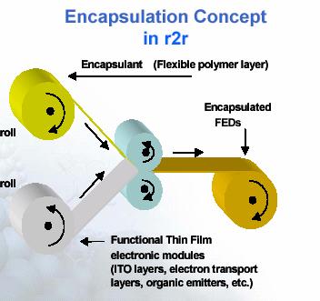
14 14
15 Functional Layers for FED* : Multi-layer stack for ultra high barrier films for display and solar applications Inorganic layers : Al 2 O 3,SiOx: Electron Beam evaporation : high rate, reasonable cost web speed e.g. 10 m/s Flexible solar medium lifetime sputtering, PECVD : best quality, higher cost e.g. 2 m/min - 0,03 m/s Flexible solar, OLED Cross-linked layer inline in vacuum or off-line at air* *e.g. ORMOCER by ISC/FhG PET Al 2 O 3 Al 2 O 3 Al 2 O 3 Al 2 O 3 *FED : Flexible Electronic Devices 15
16 Modular Roll Coater Unwind Module Process Module Rewind Module 1 Process Module with 3 Process Stations e.g. sputtered Al 2 O 3 for barrier layers Unwind Module Process Module 1 Process Module 2 Rewind Module 2 Process Modules, 6 Process Stations 16 * TM

17 SMARTWEB TM 2 Process Modules, 6 Process Stations 17

18 Sputter Deposition Sources planar and rotatable cathodes for Metals,TCO, Oxides 18
19 Ellipsometric inline control for electron beam and sputtering systems Photometry R Ellipsometry offers new possibilities:. Ellipsometry n, k separate : Ψ, Absorption ( SiOx) Layer thickness Possible relations to : T thickness + composition Density Layer-properties 19


20 Utilization of an ellipsometer in a sputter system For single layers and multilayer systems (future) 20


21 Ellipsometer installed in a modular sputter system lamp and modulator of the UFMWE* *(Ultra Fast Multi Wavelength Ellipsmeter by Jobin) Monochromator of ellipsometer receiver Chamber with roller for stable measurement 21


22 Advanced inline measurement by ellipsometer in a high speed electron beam evaporation system Installation of the ultra fast multi-wavelength ellipsometer in a high rate evaporation electron beam system Monochromator Modulator Dangerous life - 3 m above ground for the Ellipsometer staff 22
23 Electron beam inline process control with the ellipsometer SiO x barrier layer on PET film with 12 µm thickness Th-actual Th-set web speed Web speed 8 m/s web speed 6 thickness [ nm ] Set 55 nm web-speed [ m/s ] Start control by web-speed thickness web-length [ m ] Set 25 nm
24 Ultra high barrier for encapsulation The development of roll to roll inline control is supported by the EU project : FLEXONICS* ( Ultra high barrier for r2r encapsulation of flexible electronics ) Multilayer-system : Inorganic layer : Al 2 O 3, SiO Cross-linked layer : on air by ORMOCER lacquer ( SiO 2 network ) first results r2r - 4 layer stack : water vapor and oxygen permeation in the order of 1 x 10 4 ** for sputtering and evaporation *Partners : University Thessalonica, Jobin/Horiba,IVV/ISC /FhG, ** g/m**2/day cc/m**2/day Alcan, Applied MaterialI,Isovolta, Siemens, Konarca, Uni. Graz, 24
25 Conclusion Advanced vacuum coating technology and the use of latest developments of inline measurement and control techniques offers new solutions for flexible solar, OLED and copy protect markets 25
26 Thank you 感謝 Danke Kansha! Gracias Gerhard Steiniger H.J. Lotz, P. Sauer Applied Materials Technology Center Alzenau - Germany Merci 26
EQUIPMENT VACUUM WEB COATING SYSTEMS ROLL-TO-ROLL ROLL-TO-ROLL
 ROLL-TO-ROLL EQUIPMENT VACUUM WEB COATING SYSTEMS ROLL-TO-ROLL VACUUM WEB COATING APPLICATIONS VON ARDENNE provides tailored web coating solutions for today s most ambitious thin-film applications on polymer
ORGANIC ELECTRONICS PROCESS DEVELOPMENT AND ENCAPSULATION TECHNOLOGIES
 FRAUNHOFER INSTITUTE FOR ORGANIC ELECTRONICS, ELECTRON BEAM AND PLASMA TECHNOLOGY FEP ORGANIC ELECTRONICS PROCESS DEVELOPMENT AND ENCAPSULATION TECHNOLOGIES 2 PROFILE Fraunhofer FEP combines research and
VACUUM WEB COATING SYSTEMS ROLL-TO-ROLL ROLL-TO-ROLL VACUUM WEB COATING SYSTEMS
 VACUUM WEB COATING SYSTEMS ROLL-TO-ROLL ROLL-TO-ROLL VACUUM WEB COATING SYSTEMS VACUUM WEB COATING APPLICATIONS VON ARDENNE provides tailored web coating solutions for today s most ambitious thin-film
P I SCALE Creating an Open Access Flexible O L E D P ilo t L in e S e r vic e
 P I SCALE Creating an Open Access Flexible O L E D P ilo t L in e S e r vic e Pavel Kudlacek pavel.kudlacek@tno.nl P I - SCALE for 2017Flex 1 Lighting c h a lle n g e L ig h t in g c h a lle n g e At least
PROCESS TECHNOLOGIES FOR ADVANCED ORGANIC ELECTRONIC DEVICES: MICRODISPLAYS, LIGHTING AND SOLAR CELLS
 PROCESS TECHNOLOGIES FOR ADVANCED ORGANIC ELECTRONIC DEVICES: MICRODISPLAYS, LIGHTING AND SOLAR CELLS Dr. Christian May Fraunhofer IPMS - Center for Organic Materials and Electronic Devices Dresden COMEDD
Advances in Roll-to-Roll Imprint Lithography for Display Applications Using Self Aligned Imprint Lithography. John G Maltabes HP Labs
 Advances in Roll-to-Roll Imprint Lithography for Display Applications Using Self Aligned Imprint Lithography John G Maltabes HP Labs Outline Introduction Roll to Roll Challenges and Benefits HP Labs Roll
Development of OLED Lighting Applications Using Phosphorescent Emission System
 Development of OLED Lighting Applications Using Phosphorescent Emission System Kazuhiro Oikawa R&D Department OLED Lighting Business Center KONICA MINOLTA ADVANCED LAYERS, INC. October 10, 2012 Outline
Present status of Roll-to-Roll Fabrication for OLED lighting
 Present status of Roll-to-Roll Fabrication for OLED lighting Michael Stanel, Tomasz Wański, Stefan Mogck Fraunhofer Institute for Organic Electronics, Electron Beam and Plasma Technology FEP AIMCAL, Web
Advanced Display Manufacturing Technology
 Advanced Display Manufacturing Technology John Busch Vice President, New Business Development Display and Flexible Technology Group September 28, 2017 Safe Harbor This presentation contains forward-looking
Challenges for OLED Deposition by Vacuum Thermal Evaporation. D. W. Gotthold, M. O Steen, W. Luhman, S. Priddy, C. Counts, C.
 Challenges for OLED Deposition by Vacuum Thermal Evaporation D. W. Gotthold, M. O Steen, W. Luhman, S. Priddy, C. Counts, C. Roth June 7, 2011 Outline Introduction to Veeco Methods of OLED Deposition Cost
New Rotary Magnetron Magnet Bar Improves Target Utilization and Deposition Uniformity
 Society of Vacuum Coaters 2013 Technical Conference Presentation New Rotary Magnetron Magnet Bar Improves Target Utilization and Deposition Uniformity John Madocks & Phong Ngo, General Plasma Inc., 546
R2R Processing of Flexible Devices
 R2R Processing of Flexible Devices Mani Thothadri, PhD Senior Director, New Business & Strategic Initiatives Display & Flexible Technologies Group Flextech June 20, 2017 Acknowledgements Dan Forster Christoph
AMOLED Manufacturing Process Report SAMPLE
 AMOLED Manufacturing Process Report SAMPLE 2018 AMOLED Manufacturing Process Report The report analyzes the structure and manufacturing process by dividing AMOLED into small & medium-sized rigid OLED,
Thin-Film Encapsulation of Organic Light Emitting Devices (OLEDs) Dr. Emilie Galand Huntsman Advanced Materials CSEM Plastic Optoelectronics - Basel
 Dr. Emilie Galand Huntsman Advanced Materials CSEM Plastic Optoelectronics - Basel") Thin-Film Encapsulation of Organic Light Emitting Devices (OLEDs) Dr. Emilie Galand CSEM Plastic Optoelectronics - Basel 25th June 2010 About Huntsman Huntsman is a global manufacturer and marketer of
Thin-Film Encapsulation of Organic Light Emitting Devices (OLEDs) Dr. Emilie Galand CSEM Plastic Optoelectronics - Basel 25th June 2010 About Huntsman Huntsman is a global manufacturer and marketer of
THE NEXT LEVEL IN ARCHITECTURAL GLASS COATING ADVANCED EQUIPMENT & PROCESS EXPERTISE ADVANCED EQUIPMENT & PROCESS EXPERTISE
 THE NEXT LEVEL IN ARCHITECTURAL GLASS COATING ADVANCED EQUIPMENT & PROCESS EXPERTISE THE NEXT LEVEL IN ARCHITECTURAL GLASS COATING ADVANCED EQUIPMENT & PROCESS EXPERTISE ARCHITECTURAL GLASS COATING REACHES
P-224: Damage-Free Cathode Coating Process for OLEDs
 P-224: Damage-Free Cathode Coating Process for OLEDs Shiva Prakash DuPont Displays, 6 Ward Drive, Santa Barbara, CA 937, USA Abstract OLED displays require the growth of inorganic films over organic films.
:: Reduce needs for heat dissipation components. :: Extend battery life in mobile products. :: Save power and reduce heat generation in TVs
 UniversalPHOLED Technology and Materials UniversalPHOLED Phosphorescent OLED technology and materials offer record-breaking performance to bring competitive advantages to your OLED display and lighting
EQUIPMENT COATING SYSTEMS FOR THIN-FILM PV THIN-FILM PHOTOVOLTAICS. SCALA VISS PIA nova GC120VCR XENIA
 THIN-FILM PHOTOVOLTAICS EQUIPMENT COATING SYSTEMS FOR THIN-FILM PV SCALA VISS PIA nova GC120VCR XENIA OUR STORY. OUR EXPERIENCE. RANGE OF APPLICATIONS VON ARDENNE provides advanced PVD coating equipment
Press Release Plastic Electronics 2013 October 8th 10th, 2013, in Dresden/Germany Hall 2, booth no. 292 (joint booth of Organic Electronic Saxony)
") Press Release Plastic Electronics 2013 October 8th 10th, 2013, in Dresden/Germany Hall 2, booth no. 292 (joint booth of Organic Electronic Saxony) Flexible OLED from the roll Tridonic Dresden and Fraunhofer
Press Release Plastic Electronics 2013 October 8th 10th, 2013, in Dresden/Germany Hall 2, booth no. 292 (joint booth of Organic Electronic Saxony) Flexible OLED from the roll Tridonic Dresden and Fraunhofer
AIXTRON in EXCILIGHT project
 AIXTRON SE AIXTRON in EXCILIGHT project Gintautas Simkus ABOUT AIXTRON 2 Who we are Headquarter based in Herzogenrath, Germany Worldwide presence with 14 sales/representatives offices and production facilities
[1.9] AMOLED 공정 Introduction OLED Materials Patterning Process Process Equipments
![[1.9] AMOLED 공정 Introduction OLED Materials Patterning Process Process Equipments](/thumbs/73/69073032.jpg "[1.9] AMOLED 공정 Introduction OLED Materials Patterning Process Process Equipments") [1.9] AMOLED 공정 1.9.1. Introduction 1.9.2. OLED Materials 1.9.3. Patterning Process 1.9.4. Process Equipments OLED : Organic Light Emitting Diode Organic EL : Organic Electroluminescent 재료및공정 재료의발광메카니즘
[1.9] AMOLED 공정 1.9.1. Introduction 1.9.2. OLED Materials 1.9.3. Patterning Process 1.9.4. Process Equipments OLED : Organic Light Emitting Diode Organic EL : Organic Electroluminescent 재료및공정 재료의발광메카니즘
OLED Technology Introduction
 OLED Technology Introduction An organic light emitting diode (OLED) consists of several semiconducting organic layers sandwiched between two electrodes at least one of them being transparent. A simplified
HB LEDs & OLEDs. Complete thin film process solutions
 HB LEDs & OLEDs Complete thin film process solutions Get off to a flying start for all your LED thin film deposition and etch processes From 2 inch to 8 inch Manual or fully automated substrate handling
Development of OLED Lighting Panel with World-class Practical Performance
 72 Development of OLED Lighting Panel with World-class Practical Performance TAKAMURA MAKOTO *1 TANAKA JUNICHI *2 MORIMOTO MITSURU *2 MORI KOICHI *3 HORI KEIICHI *4 MUSHA MASANORI *5 Using its proprietary
Content. Core Technology (Short introduction) LCMO (Light Controlled Molecular Orientation) technology
 LCMO (Light Controlled Molecular Orientation) technology") Content Core Technology (Short introduction) LCMO (Light Controlled Molecular Orientation) technology LCMO Patterned Films for Light management : Applications Examples LCMO- Photo Patterned Retarders LCMO-
Content Core Technology (Short introduction) LCMO (Light Controlled Molecular Orientation) technology LCMO Patterned Films for Light management : Applications Examples LCMO- Photo Patterned Retarders LCMO-
GENCOA Key Company Facts. GENCOA is a private limited company (Ltd) Founded 1995 by Dr Dermot Monaghan. Located in Liverpool, UK
 Founded 1995 by Dr Dermot Monaghan. Located in Liverpool, UK") GENCOA Key Company Facts GENCOA is a private limited company (Ltd) Founded 1995 by Dr Dermot Monaghan Located in Liverpool, UK Employs 34 people 6 design (Pro E 3D CAD) 4 process development & simulation
GENCOA Key Company Facts GENCOA is a private limited company (Ltd) Founded 1995 by Dr Dermot Monaghan Located in Liverpool, UK Employs 34 people 6 design (Pro E 3D CAD) 4 process development & simulation
Improvements in Gridless Ion Source Performance
 Improvements in Gridless Ion Source Performance R.R. Willey, Willey Consulting, Melbourne, FL Keywords: Ion Beam Assisted Deposition (IBAD); Ion source; Reactive depositon ABSTRACT Ion Assisted Deposition
CORONA & PLASMA FOR NARROW WEB
 CORONA & PLASMA FOR NARROW WEB Corona & Plasma for NARROW WEB The Corona surface treatment is essential in label printing. When the label is made from plastic substrate the ink tends to become blemished
Discrete Mode Laser Diodes emitting at l~689 and 780nm for Optical Atomic clock applications.
 Discrete Mode Laser Diodes emitting at l~689 and 780nm for Optical Atomic clock applications. Richard Phelan*, M. Gleeson, J. O'Carroll, D. Byrne, L. Maigyte, R. Lennox, K. Carney. J. Somers and B.Kelly
Rotating PVD Cathodes with Lifetime Guarantee
 Rotating PVD Cathodes with Lifetime Guarantee or Current New Developments in the π-technology PLATIT AG, Selzach, Switzerland Figure 1: Series 11 - Standard PLATIT coating equipment with rotating cathodes.
CORONA & PLASMA FOR NARROW WEB
 CORONA & PLASMA FOR Corona & Plasma Corona & Plasma for Specifications Pullout Width Ozone Exhaust The Corona surface treatment is essential in label printing. When the label is made from plastic substrate
projectors, head mounted displays in virtual or augmented reality use, electronic viewfinders
 Beatrice Beyer Figure 1. (OLED) microdisplay with a screen diagonal of 16 mm. Figure 2. CMOS cross section with OLED on top. Usually as small as fingernails, but of very high resolution Optical system
OLED ON CMOS: WHAT ABOUT THINNING AND BENDING?
 Large cost-effective OLED microdisplays and their applications OLED ON CMOS: WHAT ABOUT THINNING AND BENDING? IDW2017 tony.maindron@cea.fr T. Maindron, B. Chambion, A. Vandeneynde, S. Gétin, M. Provost,
Imagine... About Us. Benefits of Rotary Cathodes. Shaping the future
 TM End Blocks e-cathode Plasma Treatment Magnetics Swing Cathode display architectural decorative solar automotive About Us Imagine... Shaping the future We take pride that our flexibility and reliability,
Application note. Materials. Introduction. Authors. Travis Burt, Huang ChuanXu*, Andy Jiang* Agilent Technologies Mulgrave, Victoria, Australia
 Performance of compact visual displays measuring angular reflectance of optically active materials using the Agilent Cary 7000 Universal Measurement Spectrophotometer (UMS) Application note Materials Authors
Screen investigations for low energetic electron beams at PITZ
 1 Screen investigations for low energetic electron beams at PITZ S. Rimjaem, J. Bähr, H.J. Grabosch, M. Groß Contents Review of PITZ setup Screens and beam profile monitors at PITZ Test results Summary
PUBLISHABLE Summary To provide OLED stacks with improved reliability Provide improved thin film encapsulation
 PUBLISHABLE Summary SCOOP is a European funded project (FP7 project number 287595 SCOOP). It is focused on OLED technology, microdisplays based on the combination of OLED with CMOS technology, and innovative
center for organic materials and electronic devices dresden
 F R A U N H O F E R I N S T I T U T e F o R P h o t o n i c M i c r o S y s t e m s I P M S center for organic materials and electronic devices dresden p r e f a c e Dr. Christian May Head of Business
THE NEW LASER FAMILY FOR FINE WELDING FROM FIBER LASERS TO PULSED YAG LASERS
 FOCUS ON FINE SOLUTIONS THE NEW LASER FAMILY FOR FINE WELDING FROM FIBER LASERS TO PULSED YAG LASERS Welding lasers from ROFIN ROFIN s laser sources for welding satisfy all criteria for the optimized laser
Present and future of OLED lighting
 Present and future of OLED lighting Dr. Wolfgang Dötter Authorized Company Officer OLEDWorks Global Q-EHS Manager & Senior Integral Project Manager 1 Vision In 10 years there will be only Solid State Lighting;
Organic light emitting diode (OLED) displays
 displays") Ultra-Short Pulse Lasers Enable Precision Flexible OLED Cutting FLORENT THIBAULT, PRODUCT LINE MANAGER, HATIM HALOUI, APPLICATION MANAGER, JORIS VAN NUNEN, PRODUCT MARKETING MANAGER, INDUSTRIAL PICOSECOND
Ultra-Short Pulse Lasers Enable Precision Flexible OLED Cutting FLORENT THIBAULT, PRODUCT LINE MANAGER, HATIM HALOUI, APPLICATION MANAGER, JORIS VAN NUNEN, PRODUCT MARKETING MANAGER, INDUSTRIAL PICOSECOND
Applied Materials. 200mm Tools & Process Capabilities For Next Generation MEMS. Dr Michel (Mike) Rosa
 Rosa") Applied Materials 200mm Tools & Process Capabilities For Next Generation MEMS Dr Michel (Mike) Rosa 200mm MEMS Global Product / Marketing Manager, Components and Systems Group (CSG), Applied Global Services
Applied Materials 200mm Tools & Process Capabilities For Next Generation MEMS Dr Michel (Mike) Rosa 200mm MEMS Global Product / Marketing Manager, Components and Systems Group (CSG), Applied Global Services
Phosphorescent OLED Technologies: The Next Wave. Plastic Electronics Conference Oct 9, 2012
 Phosphorescent OLED Technologies: The Next Wave Plastic Electronics Conference Oct 9, 2012 UDC Company Focus IP innovator, technology developer, patent licensor and materials supplier for the rapidly growing
Solution Processable OLEDs. Anna Hayer EuroDisplay /09/2013
 Solution Processable LEDs Merck KGaA Anna Hayer EuroDisplay 2013 Content 1 Introduction 2 LED Basics 3 Challenges for Solution Processing 4 Current Results 5 Summary 2 EuroDisplay 2013 Hayer - Merck Solution
Illumination Challenges in Non- Industrial Vision Applications. Simon Stanley Managing Director ProPhotonix IRL Ltd
 Illumination Challenges in Non- Industrial Vision Applications Simon Stanley Managing Director ProPhotonix IRL Ltd ProPhotonix designs and manufactures high-quality LED systems and laser modules for the
Flexible and transparent OLED device. July, Lead author: Robert Abbel, Holst Center / TNO Pim Groen, Holst Center / TNO
 Flexible and transparent OLED device July, 2016 Lead author: Robert Abbel, Holst Center / TNO Pim Groen, Holst Center / TNO Aito Interactive Oy Bax & Willems Brunel University Diffus Design IS Fjord Spain
IGM. Development of Vapor Deposition Processes for OLEDs. Bachelor Thesis. Prof. Dr.-Ing. N. Frühauf. 28th of September Alexandru Andrei Lungu
 IGM Institut für Großflächige Mikroelektronik Institut für Großflächige Mikroelektronik Prof. Dr.-Ing. N. Frühauf Development of Vapor Deposition Processes for OLEDs Bachelor Thesis 28th of September 2014
Digital Light Processing
 A Seminar report On Digital Light Processing Submitted in partial fulfillment of the requirement for the award of degree of Bachelor of Technology in Computer Science SUBMITTED TO: www.studymafia.org SUBMITTED
High Performance White OLEDs Technologies for Lighting
 High Performance White OLEDs Technologies for Lighting 10 October, 2012 Takuya Komoda Core Technologies Development Center Panasonic Corporation Contents 2 1. Expectation to the Next Generation Lighting
Development and Mass-Production of an OLED Lighting Panel - Most-Promising Next-Generation Lighting -
 Development and Mass-Production of an OLED Lighting Panel - Most-Promising Next-Generation Lighting - 47 KEIICHI HORI *1 JOJI SUZUKI *2 MAKOTO TAKAMURA *3 JUNICHI TANAKA *4 TSUTOMU YOSHIDA *5 YOSHITAKA
Polygon Scanners Capabilities, Applications and System integration. considerations
 Workshop ALPS Swissphotonics - APPOLO Polygon Scanners Capabilities, Applications and System integration considerations Lars Penning CEO Next Scan Technology Innovating and leading polygon scanner technology
(12) (10) Patent No.: US 7,133,032 B2. Cok (45) Date of Patent: Nov. 7, 2006
 (10) Patent No.: US 7,133,032 B2. Cok (45) Date of Patent: Nov. 7, 2006") United States Patent US007133032B2 (12) (10) Patent No.: Cok (45) Date of Patent: Nov. 7, 2006 (54) OLED DISPLAY AND TOUCH SCREEN 6,762,747 B1 * 7/2004 Fujioka et al.... 345,157 6,846,579 B1* 1/2005 Anderson
United States Patent US007133032B2 (12) (10) Patent No.: Cok (45) Date of Patent: Nov. 7, 2006 (54) OLED DISPLAY AND TOUCH SCREEN 6,762,747 B1 * 7/2004 Fujioka et al.... 345,157 6,846,579 B1* 1/2005 Anderson
World Class Converting Xpanded Productivity Platform Xpanded Capabilities State-of-the-Art Ergonomics
 World Class Converting Xpanded Productivity Platform Xpanded Capabilities State-of-the-Art Ergonomics MULTI-PROCESS CAPABILITIES GENUINE PLATFORM SERVO PRESS When Mark Andy set out to offer one of the
Toward Novel Flexible Display Top-Emitting OLEDs on Al-Laminated PET Substrates
 Toward Novel Flexible Display Top-Emitting OLEDs on Al-Laminated PET Substrates FURONG ZHU, XIAO-TAO HAO, ONG KIAN SOO, YANQING LI, AND LI-WEI TAN Contributed Paper We developed a flexible organic LED
Scalable self-aligned active matrix IGZO TFT backplane technology and its use in flexible semi-transparent image sensors. Albert van Breemen
 Scalable self-aligned active matrix IGZO TFT backplane technology and its use in flexible semi-transparent image sensors Albert van Breemen Image sensors today 1 Dominated by silicon based technology on
Customer Responsibilities. Important Customer Information. Agilent InfinityLab LC Series Site Preparation Checklist
 Agilent Site Preparation InfinityLab Checklist LC Series Thank you for purchasing an Agilent instrument. To get you started and to assure a successful and timely installation, please refer to this specification
Defect Analysis of Roll-to-Roll SAIL Manufactured Flexible Display Backplanes
 Defect Analysis of Roll-to-Roll SAIL Manufactured Flexible Display Backplanes Carl Taussig, Richard E. Elder, Warren B. Jackson, Albert Jeans, Mehrban Jam, Ed Holland, Hao Luo, John Maltabes, Craig Perlov,
High Power Efficiencies at Record Lifetimes: NOVALED s PIN-OLEDs
 High Power Efficiencies at Record Lifetimes: NOVALED s PIN-OLEDs Harald Gross, Jan Blochwitz-Nimoth, Jan Birnstock, Ansgar Werner, Michael Hofmann, Philipp Wellmann, Tilmann Romainczyk, Sven Murano, Andrea
The Company. A leading OLED player
 The Company A leading OLED player Novaled is the company to trade with, work for and invest in. Our company focuses on proprietary organic materials and complementary innovative technologies for superior
25W 9xxnm Uncooled Multimode Laser Diode Module
 25W 9xxnm Uncooled Multimode Laser Diode Module BMU25-9xx-01/02-R Features: Single emitter based laser diode module High output power of 25W 0.15NA or 0.22NA 105μm core multimode optical fiber Hermetically
Data. X-ray Image Intensifier HIDEQ 23-3 ISP
 Data X-ray Image Intensifier HIDEQ 23-3 ISP State-of-the-art Image Intensifier Technology HIDEQ 23-Mu Features and benefits HDQE cesium iodide input phosphor screen of very fine structure deposited on
Silole Derivative Properties in Organic Light Emitting Diodes
 Silole Derivative Properties in Organic Light Emitting Diodes E. Duncan MLK HS Physics Teacher Mentors: Prof. Bernard Kippelen & Dr. Benoit Domercq Introduction Theory Methodology Results Conclusion Acknowledgements
ADDING AN O TO LEDS STATUS AND PERSPECTIVES OF ORGANIC LIGHT EMITTING DIODES PAWEL E. MALINOWSKI, TUNGHUEI KE LED EVENT 2017
 ADDING AN O TO LEDS STATUS AND PERSPECTIVES OF ORGANIC LIGHT EMITTING DIODES PAWEL E. MALINOWSKI, TUNGHUEI KE LIVING ROOM NOT SO LONG AGO... 2 Source: Warner Bros. Incadescent CRT 3 Source: Warner Bros.
Overcoming Challenges in 3D NAND Volume Manufacturing
 Overcoming Challenges in 3D NAND Volume Manufacturing Thorsten Lill Vice President, Etch Emerging Technologies and Systems Flash Memory Summit 2017, Santa Clara 2017 Lam Research Corp. Flash Memory Summit
Korea Coating Materials & Components Co., Ltd. Company Introduction.
 Korea Coating Materials & Components Co., Ltd. Company Introduction www.kcmc.biz Profile for KCMC Co., LTD CEO: Yeom, Jung-Hoon Founded: 15 th July 2010 Employees: 13 Application: Rotatable & Planar type
High Value Applications and High Growth Markets for Printed Electronics
 High Value Applications and High Growth Markets for Printed Electronics Marc Chason Marc Chason and Associates, Inc. marcchason@sbcglobal.net October 5, 2011 Why SSL for Printed Electronics? Four Themes
OLED for Lighting. Outline
 OLED for Lighting Monica Katiyar MME & SCDT Indian Institute of Technology, Kanpur Outline Lighting Photometry and colorimetry Some examples Various approaches to W-OLED 1 500,000 years ago Lighting Gas
VTA1216H Series Linear Photodiode Array (PDA) for X-ray Scanning
 for X-ray Scanning") DATASHEET Photon Detection VTA1216H Series VTA1216H-L-SC-08-1 The VTA1216H series is a 16-channel High Resolution Photodiode Array (PDA). There are 8 dual-element photodiodes mounted directly on an FR-4
DATASHEET Photon Detection VTA1216H Series VTA1216H-L-SC-08-1 The VTA1216H series is a 16-channel High Resolution Photodiode Array (PDA). There are 8 dual-element photodiodes mounted directly on an FR-4
OLED Lighting in Automotive Applications State of the Art and Future Demands. OLEDs World Summit 2017, San Francisco, Dr. Werner Thomas, AUDI AG
 OLED Lighting in Automotive Applications State of the Art and Future Demands OLEDs World Summit 2017, San Francisco, Dr. Werner Thomas, AUDI AG 2 Agenda 1. Overview 1 st automotive series applications
Teaching Plasma Nanotechnologies Based on Remote Access
 Teaching Plasma Nanotechnologies Based on Remote Access Authors: Alexander Zimin, Bauman Moscow State Technical University, Russia, zimin@power.bmstu.ru Andrey Shumov, Bauman Moscow State Technical University,
Pressure sensor. Surface Micromachining. Residual stress gradients. Class of clean rooms. Clean Room. Surface micromachining
 Pressure sensor Surface Micromachining Deposit sacrificial layer Si PSG By HF Poly by XeF2 Pattern anchors Deposit/pattern structural layer Etch sacrificial layer Surface micromachining Structure sacrificial
Leading. Through Innovation. Film Technology Franchise. September 9, 2008
 Film Technology Franchise Steven Webster, VP, Research & Technology Commercialization Display & Graphics Business Leading Through Innovation September 9, 2008 1 3M s Film Franchise Is More Than Optical
SUPPLEMENTARY INFORMATION
 User-interactive electronic-skin for instantaneous pressure visualization Chuan Wang 1,2,3, David Hwang 1,2,3, Zhibin Yu 1,2,3, Kuniharu Takei 1,2,3, Junwoo Park 4, Teresa Chen 4, Biwu Ma 3,4, and Ali
General Specifications
 General Specifications WG41F11C Compact O Frame GS 14M04B10-20E-Z1 [Style: S1] Overview The WG41F11C Compact O frame is a space-saving frame designed for coating lines of battery electrode sheets. This
New Worlds for Polymers: Organic Transistors, Light Emitting Diodes, and Optical Waveguides Ed Chandross
 New Worlds for Polymers: Organic Transistors, Light Emitting Diodes, and Optical Waveguides Ed Chandross Materials Chemistry, LLC 1 Polymers in the Electronic Industry Enabling Materials Active Materials?
FRAUNHOFER INSTITUTE FOR ORGANIC ELECTRONICS, ELECTRON BEAM AND PLASMA TECHNOLOGY FEP
 PRESSEINFORMATION Flexible OLED applications arrive June 22, 2016 Page 1 / 7 R2D2, a joint project to analyze and development high-trl processes and technologies for manufacture of flexible organic light-emitting
High Repetition Rate USP Lasers Improve OLED Cutting Results
 Coherent White Paper May 7, 2018 High Repetition Rate USP Lasers Improve OLED Cutting Results High power ultraviolet, picosecond industrial lasers are widely employed because of their proven ability to
 Page 1 of 8 Main > Electronics > Computers How OLEDs Work by Craig Freudenrich, Ph.D. Introduction to How OLEDs Work Imagine having a high-definition TV that is 80 inches wide and less than a quarter-inch
MEMS Technologies Dresden - Product Development and Fabrication at IPMS Dresden
 MEMS Technologies Dresden - Product Development and Fabrication at IPMS Dresden MEMS Technologies Dresden - Product Development and Fabrication at IPMS Dresden Michael Müller, Matthias List Outline FhG-IPMS
THE challenges facing today s mobile
 MEMS displays MEMS-Based Display Technology Drives Next-Generation FPDs for Mobile Applications Today, manufacturers of mobile electronic devices are faced with a number of competitive challenges. To remain
CHA EVAPORATOR. User guidelines. p.1. by Carlos Manzanedo. Last revised: 10/05/2000
 CHA EVAPORATOR User guidelines by Carlos Manzanedo. Last revised: 10/05/2000 p.1 Introduction. The CHA evaporator has the following characteristics: 1. 2 independent resistive power supplies. 2. 1 Electron
CHA EVAPORATOR Short Reference User guidelines
 CHA EVAPORATOR Short Reference User guidelines by Carlos Manzanedo. Last revised: 10/05/2000 p.1 Procedure: The CHA evaporator is divided into 16 different panels. These panels are labeled on the machine
Flexible Electronics Production Deployment on FPD Standards: Plastic Displays & Integrated Circuits. Stanislav Loboda R&D engineer
 Flexible Electronics Production Deployment on FPD Standards: Plastic Displays & Integrated Circuits Stanislav Loboda R&D engineer The world-first small-volume contract manufacturing for plastic TFT-arrays
An Overview of OLED Display Technology
 page:1 An Overview of OLED Display Technology Homer Antoniadis OSRAM Opto Semiconductors Inc. San Jose, CA page:2 Outline! OLED device structure and operation! OLED materials (polymers and small molecules)!
Modular screen printing system from 2 6 colours
 THIEME 5000 multicolour line Modular screen printing system from 2 6 colours THIEME 5000 multicolour line Details of the THIEME 5000 multicolour line Modular profile chassis construction Grippers and Gripper
Transforming Electronic Interconnect Breaking through historical boundaries Tim Olson Founder & CTO
 Transforming Electronic Interconnect Breaking through historical boundaries Tim Olson Founder & CTO Remember when? There were three distinct industries Wafer Foundries SATS EMS Semiconductor Devices Nanometers
Quantum Dot Solutions for Lighting and Display Applications. Frank Ignazzitto APEC Conference February 9, 2012
 Quantum Dot Solutions for Lighting and Display Applications Frank Ignazzitto APEC Conference February 9, 2012 QD Vision s Focused & Integrated Approach The only quantum dot company focused solely on displays
Electron Beam Technology
 Electron Beam Technology Speed up! High Performance Electron Beam Lithography dedicated electron beam lithography To bridge cutting-edge research and nanofabrication, a dedicated nanolithography solution
Electroluminescent Light Sources. By Michael Dierks
 Electroluminescent Light Sources By Michael Dierks Table of contents Overview on Electroluminescent Light Sources Powder Electroluminescens History Strucure of an ac powder based EL device Mechanism The
ADVANCEMENTS IN GRAVURE TECHNOLOGY: FOR SUSTAINABILITY AND GROWTH PRINTED LIGHTING TECHNOLOGY
 ADVANCEMENTS IN GRAVURE TECHNOLOGY: FOR SUSTAINABILITY AND GROWTH PRINTED LIGHTING TECHNOLOGY Marc Chason Marc Chason and Associates, Inc. marcchason@sbcglobal.net January 17, 2012 Logic Driven Value Chain
Advanced Sensor Technologies
 Advanced Sensor Technologies Jörg Amelung Fraunhofer Institute for Photonics Microsystems Name of presenter date Sensors as core element for IoT Next phase of market grow New/Advanced Requirements based
Vinfoil Infigo SF110 UFC module for UV Film Casting application
 Vinfoil Infigo SF110 UFC module for UV Film Casting application 1 2 What is UV Film Casting (UFC) The Cast and Cure process uses a holographic film in combination with a UV coating on any substrate to
IOSR Journal of Engineering (IOSRJEN) ISSN (e): , ISSN (p): Volume 2, PP Organic Led. Figure 1.
 ISSN (e): , ISSN (p): Volume 2, PP Organic Led. Figure 1.") IOSR Journal of Engineering (IOSRJEN) ISSN (e): 2250-3021, ISSN (p): 2278-8719 Volume 2, PP 46-51 www.iosrjen.org Organic Led Prof.Manoj Mishra 1, Sweety Vade 2,Shrutika Sawant 3, Shriwari Shedge 4, Ketaki
IOSR Journal of Engineering (IOSRJEN) ISSN (e): 2250-3021, ISSN (p): 2278-8719 Volume 2, PP 46-51 www.iosrjen.org Organic Led Prof.Manoj Mishra 1, Sweety Vade 2,Shrutika Sawant 3, Shriwari Shedge 4, Ketaki
Leveraging 300 mm Technology Solutions to Enable New MEMS Process Capabilities
 Leveraging 300 mm Technology Solutions to Enable New MEMS Process Capabilities Evan Patton Semicon Europa November 2017 Lam Research Corp. 1 Presentation Outline The Internet of Things (IoT) as a market
Display Technologies CMSC 435. Slides based on Dr. Luebke s slides
 Display Technologies CMSC 435 Slides based on Dr. Luebke s slides Recap: Transforms Basic 2D Transforms: Scaling, Shearing, Rotation, Reflection, Composition of 2D Transforms Basic 3D Transforms: Rotation,
VTA0832H Series Linear Photodiode Array (PDA) for X-ray Scanning
 for X-ray Scanning") DATASHEET Photon Detection VTA0832H Series VTA0832H-L-NC-00-0 The VTA0832H series is a 32-channel High Resolution Photodiode Array (PDA). There are 16 dual-element photodiodes mounted directly on an FR-4
DATASHEET Photon Detection VTA0832H Series VTA0832H-L-NC-00-0 The VTA0832H series is a 32-channel High Resolution Photodiode Array (PDA). There are 16 dual-element photodiodes mounted directly on an FR-4
Parts of dicing machines for scribing or scoring semiconductor wafers , , , , ,
 US-Rev3 26 March 1997 With respect to any product described in or for Attachment B to the Annex to the Ministerial Declaration on Trade in Information Technology Products (WT/MIN(96)/16), to the extent
Characterization and Performance of Multiple Gridless Ion Sources for Wide-area Ion Beam Assisted Processes Applications
 Characterization and Performance of Multiple Gridless Ion Sources for Wide-area Ion Beam Assisted Processes Applications L. Mahoney, T. Alexander, and D. Siegfried, Veeco Instruments Inc., Fort Collins,
The Transition to Patterned Media in Hard Disk Drives
 The Transition to Patterned Media in Hard Disk Drives The Evolution of Jet and Flash Imprint Lithography for Patterned Media DISKCON San Jose Sept 24 rd, 2009 Paul Hofemann, Vice President, HDD Future